
Manipulating the distribution of photo-induced electrons on semiconductor surfaces is meaningful to develop novel optoelectronic technologies. Yet, it is a challenging task due to the lack of feasible methods. Keshav M. Dani and co-workers from Okinawa Institute of Science and Technology, Japan, have filled the niche. They demonstrated that a beam of ultrafast light pulse could pull apart the photo-induced electrons on a GaAs semiconductor surface. This study was recently published in Science Advances (doi:10.1126/sciadv.aat9722).
The ability to record movies of ultrafast charge transport in semiconductors with an advanced time-resolved photoemission electron microscope (TR-PEEM) inspired this work. This unique microscope developed within this research group can image surface electron motion in semiconductors with high spatial and temporal resolution. “Using our TR-PEEM, last year we recorded a movie of electrons moving across a semiconductor heterojunction,” says E. Laine Wong of Okinawa Institute of Science and Technology, the first author of the article. “We then wanted to see if we could drive the motion of electrons in a homogeneous semiconductor by utilizing intensity variations in an optical pulse.”
(a) The illustration of the surface photovoltage effect that leads to the surface potential variation; (b) the evolution of the surface-electron distribution profile into two separated Gaussian peaks within 500 ps after photoexcitation. Credit: Science Advances.
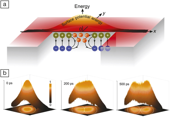
The technique used to separate the surface photo-induced electrons is based on the surface photovoltage effect. Upon shining a light pulse from a laser source onto a p-type semiconductor, where the light pulse has higher energy than the semiconductor’s bandgap, electrons and holes will be generated near the semiconductor surface. The subsequent drift of the photo-induced electrons toward the surface weakens the intrinsic electric field in the semiconductor and results in a lateral surface potential difference. This potential difference then drives the surface photo-induced electrons apart. Specifically, the researchers irradiated a p-type Zn-doped GaAs semiconductor with an excitation pulse having a Gaussian-shaped intensity profile. This irradiation divided the photo-induced electrons into two groups over 500 ps after a 45-fs photoexcitation.
The rate and the degree of the transient electron separation depended on the concentration of the charge carriers (photo-induced electrons and holes). With a relatively low charge-carrier density of 2.8 × 1018 cm–3, the distribution profile of the surface electrons only developed into a single flat-top Gaussian peak; that is, the surface electrons were not separated. At charge-carrier densities of 8.4 × 1018 cm–3 and above, the surface electron redistributed into two groups, as evidenced from the two separated Gaussian peaks. Additionally, the peak separation broadened with elevated charge-carrier density because higher charge-carrier density led to stronger lateral surface potential that forced the surface electrons apart.
Mingyang Li of Sun Yat-sen University, China, who is not involved in the work, says, “The capability of imaging the charge transport on semiconductor surfaces with excellent resolutions could verify the simulated motions of photocarriers during photo-reactions. The manipulation of the photo-induced electron distribution might also be used to improve the performance of photoelectrochemical cells.”
