

1. Introduction
Nowadays, ultra-violet (UV) and blue light emitting nitride semiconductor lasers based on wide-gap GaN, AlN, and InN semiconductor materials and their solid solutions Reference Strite and Morkoç[1], are attracting considerable attention. This is due to possibly wide applications of these lasers, especially in high-density optical recording devices Reference Terris, Mamin and Rugar[2], and the printing and imaging industry. Recent technology advancements for nitride lasers, achieved primarily by Shuji Nakamura with his co-workers from Nichia Chemical Industries, Ltd., has resulted in immediate progress in laser performance. Only 12 months after the first announcement, at the beginning of 1996 Reference Nakamura, Senoh, Nagahama, Iwasa, Yamada, Matsushita, Kiyoku and Sugimoto[3], of pulsed operation of nitride lasers at room temperature (RT), the first RT continuous-wave (CW) operation was obtained Reference Nakamura, Senoh, Nagahama, Iwasa, Yamada, Matsushita, Sugimoto and Kiyoku[4]. Initially, the lifetime of these first RT CW nitride lasers was extremely short, but it was extended to 35 hours by the end of 1996 Reference Nakamura[5] and a potential 10,000 hours of RT CW operation was reported recently Reference Nakamura, Senoh, Nagahama, Iwasa, Yamada and Matsushita[6], another 12 months later.
The latest Nichia achievements Reference Nakamura, Senoh, Nagahama, Iwasa, Yamada and Matsushita[6] are very promising but a high density of defects in their GaN devices Reference Lester, Ponce, Craford and Steigerwald[7] seems to be still an unsolved problem in edge-emitting lasers (EELs). These difficulties might be resolved in nitride vertical-cavity surface-emitting lasers (VCSELs) due to the relatively small volumes of their active regions Reference Pankove[8]. Also, the serious difficulties in manufacturing smooth highly-reflective mirrors of EELs may be relatively easy to overcome in VCSELs with semiconducting distributed Bragg reflectors (DBRs). However, there have been only a few successful attempts to fabricate optically pumped VCSELs Reference Redwing, Loeber, Anderson, Tischler and Flynn[9] Reference Asif Khan, Krishnankutty, Skogman, Kuznia, Olson and George[10]. The reason for this is probably associated with the very high end losses of VCSELs in comparison to EELs. Nevertheless, because of their unique properties VCSEL structures are unquestionably an inevitable future of nitride lasers. Therefore, an analysis of their RT operation will be helpful in optimization of their possible configurations.
To the authors' best knowledge, the only threshold estimation for RT operation of nitride VCSELs was reported by T. Honda et al. Reference Honda, Katsube, Sakaguchi, Koyama and Iga[11]. While their optical gain calculations seem to be very reasonable, their optical loss analysis suffers from many drawbacks and unnecessary assumptions leading to inaccurate and very underestimated threshold current densities. In the present paper, careful threshold analysis is reported for a pulsed RT operation of UV-emitting nitride VCSELs with bulk, single-quantum-well and multiple-quantum well active regions. The analysis is based on recent experimental and theoretical published results.
2. The Model
The analysis does not include thermal and current-spreading effects, therefore, it is carried out for RT pulsed nitride VCSEL operation of the top-emitting VCSEL structure presented in Figure 1. Current-leakage effects are also neglected in this simulation.
A schematic structure of the considered nitride VCSEL.

Three types of GaN active regions are taken into consideration:
-
• bulk GaN active region,
-
• GaN/Al0.2Ga0.8N single-quantum-well (SQW) active region,
-
• GaN/Al0.2Ga0.8N multiple-quantum-well (MQW) active region.
GaN active regions (instead of the InGaN active regions usually used in nitride EELs) were chosen intentionally to shift laser emission bands to lower wavelengths, for which material absorption in AlGaN layers is much lower. This kind of absorption may be considerably reduced in nitride EELs where penetration of cladding AlGaN layers by stimulated radiation is limited by their much lower refractive indices. It is, however, unavoidable in nitride VCSELs, in which stimulated radiation is traveling across AlGaN spacers. Both (P-type and N-type) spacers are assumed to be fabricated from Al0.1Ga0.9N and both DBR mirrors - from AlN/Al0.15Ga0.85N.
The lasing threshold condition may be written in the following form Reference Mroziewicz, Bugajski and Nakwaski[12]
where Γi and α i (i = A,P,N) are, respectively, the confinement factors and losses in corresponding layers, L is the resonator length, R F and R R are the reflectivities of the front (output) and the rear resonator mirrors, respectively, g th is the threshold optical gain, and ΓM and α M will be defined later.
In determining the resonator length L(L= d A + d N + d P + l N + l P), not only the thicknesses of the active region (d A) and the N-type (d N) and the P-type (d P) cladding layers should be taken into account, but also the energy penetration depths of the N-type (l N) and the P-type (l P) DBR mirrors. The latter thicknesses can be determined with the aid of the formulae derived by D. I. Babic and S. W. Corzine Reference Babic and Corzine[13].
Assuming a uniform intensity distribution within the laser resonator, the confinement factors may be easily expressed as
for i = A, P, N respectively. At normal incidence, a periodic structure of quarter-wave-thick layers exhibits the following reflectivity Reference Born and Wolf[14]:

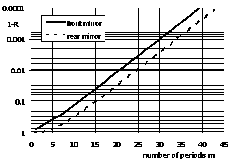
where m is the number of periods in the mirror, n 1 and n m are the refractive indices of the medium on the transmitted and incident sides of the DBR mirror, and n L and n H stand for the refractive indices of alternate sections of the mirror. For the rear N-type DBR, the transmitted medium is the substrate, and the incident one is the spacer whereas for the output P-type DBR they are the external medium (air) and again the spacer, respectively. Their reflectivities for the rear N-type DBR (R R) and for the output P-type DBR (R F) are directly associated with their numbers (m R and m F, respectively) of periods of alternate layers.
Following the approach of D. I. Babic et al. Reference Babic, Chung, Dagli and Bowers[15], diffraction losses αdiff for the UV laser may be found from their Figure 4 with Fresnel number N F:
where r A stands for the active-region radius, λ 0 is the design wavelength and n i is the refractive index of the spacer. For the laser structure under consideration (c.f. Figure1), diffraction losses were found to be equal to 0.03/L for r A=2.5 μm, 0.016/L for r A = 3 μm, 0.002/L for r A = 5 μm and 0.001/L for r A = 7 μm.
In conventional diode lasers manufactured in both the GaAs/AlGaAs and the InP/InGaAsP systems, material losses in cladding layers may be completely neglected. Optical measurements of nitrides Reference Yu, Wang, Ishikawa, Umeno, Soga, Egawa, Watanabe and Jimbo[16] Reference Chichibu, Mizutani, Shioda, Nakanishi, Deguchi, Azuhata, Sota and Nakamura[17] Reference Fischer, Shan, Song, Chang, Horning and Goldenberg[18] Reference Bougrov and Zubrilov[19] reveal, however, long tails of density of states extending deeply into the band gap. Therefore active-region losses are mainly free-carrier losses:
whereas optical losses in spacers contain also material losses αm,P and αm,N Reference Yoshida, Misawa and Gonda[20] Reference Frankowski, Steuber, Härle, Scholz and Hangleiter[21]:
In ideal cladding layers, these are negligible, increasing, however, very quickly with deterioration of crystallographic perfection. Unexpectedly high material losses reported for AlGaN layers (see e.g. Figure 2 in Reference Ambacher, Arzberger, Brunner, Angerer, Freudenberg, Esser, Wethkamp, Wilmers, Richter and Stutzmann[22]) are probably a result of their spatially nonuniform compositions (and maybe also, but to smaller extent, inhomogeneous doping levels). In the model, we also take into account material losses in the DBR mirrors (α M) within the energy penetration depths (l N and l P). Strictly speaking, we assume these losses to be confined to the Al0.15Ga0.85N layers (ΓM) because of the much wider energy gap of the AlN layers.
Dependence of the C Auger recombination coefficient of many semiconductor materials Reference Landolt-Börnstein[50] on their electron effective masses, m e. The extrapolation giving the C value (C GaN = 1.4.10−31 cm6s−1) is shown. m e,GaN = 0.22m 0 is taken from Ref. Reference Frankowski, Steuber, Härle, Scholz and Hangleiter[21]. m 0 is the electron rest mass.

For the wavelength of 370 nm and the spacer composition Al0.1Ga0.9N, the reported values of material absorption range from 10 cm−1 Reference Yoshida, Misawa and Gonda[20] up to as much as 500 cm−1 Reference Bougrov and Zubrilov[19] Reference Ambacher, Arzberger, Brunner, Angerer, Freudenberg, Esser, Wethkamp, Wilmers, Richter and Stutzmann[22]. Free-carrier losses were deduced from Figure 3 in Ref. Reference Pankove, Bloom and Harbeke[23] to be equal to about 1 cm−1.
Reflectivity of the front (R F) and the rear (R R) AlN/Al0.15Ga0.85N DBR mirrors versus number m of their periods
Light scattering by edge dislocations has been found by L. Liau et al. Reference Liau, Aggarwal, Maki, Molnar, Walpole, Williamson and Melngailis[24] to be a crucial optical loss mechanism in nitride layers. According to the paper of S. D. Lester et al. Reference Lester, Ponce, Craford and Steigerwald[7], spectacular blinding blue LEDs manufactured by Nichia surprisingly contained as many as 1010 to 1011 dislocations per cm2. Even for a relatively low dislocation density N D = 2·1010 cm−2, scattering losses α scatt as high as 300 cm−1 were found Reference Liau, Aggarwal, Maki, Molnar, Walpole, Williamson and Melngailis[24]. To decrease them to an acceptable range of 5 cm−1, the dislocation density N D must be reduced to as low as 3·108 cm−2 Reference Liau, Aggarwal, Maki, Molnar, Walpole, Williamson and Melngailis[24]. A larger reduction was reported very recently using the lateral epitaxial overgrowth method of growing GaN layers Reference Zheleva, Nam, Bremser and Davis[25]. This technique is expected to lower the dislocation density by at least 3−4 orders of magnitude Reference Marchand, Ibbetson, Fini, Kozodoy, Keller, DenBaars, Speck and Mishra[26]. If so, then the corresponding scattering losses could be neglected.
Mirror losses αM are associated with light scattering and absorption within the DBR-mirrors because of imperfections of their structure, including material absorption inside their layers, absorption on layer edges, scattering by material imperfections (e.g. dislocations) and scattering because of non-uniform layer thicknesses. They are difficult to determine, so for simplicity, they were incorporated in the model by assuming scattering (α scatt ) and absorption losses (αm,P, αm,N) within energy penetration depths of both resonator mirrors. It should be remembered, however, that mirror losses start growing quickly after exceeding some number of structure periods, depending on the technology or equipment used. So they ought to be taken into account when optimizing the structure of nitride lasers (c.f. 30-period Al0.4Ga0.6N/Al0.12Ga0.88N Bragg reflectors reported by J. M. Redwing et al. Reference Redwing, Loeber, Anderson, Tischler and Flynn[9]).
The maximum optical gain in a bulk active region may be written as
whereas for a single-quantum-well active region, a logarithmic relation in the following form is often used:
In the above expressions, a is the differential gain, n stands for the carrier concentration, n tr is the transparency concentration, and b is a coefficient directly proportional to a. Following the approach of A. T. Meney and E. P. O'Reilly Reference Meney and O’Reilly[27] and T. Honda et al. Reference Honda, Katsube, Sakaguchi, Koyama and Iga[11] for the bulk GaN active region, we found: n tr = 0.75·1019 cm−3 and a = 2.5·10−16 cm2. Values of analogous parameters for single and multiple GaN quantum well active regions are obtained from data reported in Ref. Reference Uenoyama and Suzuki[28] and are listed in Table 1. The lowest threshold was found for an active region thickness of 4 nm (n tr = 1.22·1019 cm−3 and b = 6.72·103 cm−1).
Gain parameters (averaged over the range g < 2000 cm−1) for a single quantum well, extracted from data given in [28].

The threshold carrier density n th may be found from Equation 1 with the threshold gain g th = g(n= n th). The threshold current density j th is directly related to n th from the following relation Reference Coldren and Corzine[29]:
where e is the electron charge, A is the monomolecular recombination coefficient (mostly associated with nonradiative recombination at point defects), B is the bimolecular recombination coefficient (principally connected with radiative recombination), and C is the Auger recombination coefficient. In InGaAsP, the A coefficient is in the range of (1−2)·108 s−1 at room temperature Reference Haug[30] Reference Zou, Osinski, Grodzinski, Dapkus, Rideout, Sharfin, Schlafer and Crawford[31] and is slowly reduced with a decrease in temperature Reference Mozer, Hausser and Pilkuhn[32], i.e. with an increase in an energy gap. Therefore we assume for GaN A= 1.0·108 s −1. The bimolecular radiative recombination coefficient B for GaN at room temperature was calculated in Ref. Reference Dmitriev and Oruzheinikov[33] (B= 0.15·1010 cm 3 s −1). Finally, a value for the Auger recombination coefficient C= 1.4·10−31 cm 6 s −1 was found using an extrapolation of the dependence of C values of many semiconductor materials on their electron effective masses (see Figure 2). In the above, we assume perfect recombination for carriers above their threshold concentration, according to suggestion of K. Petermann Reference Petermann[34].
In case of MQW active layers, homogeneous injection of carriers in all quantum wells is assumed Reference Yeo, Chong, Li and Fan[35] and the cumulative thickness of the active region is just the sum of the thicknesses of all the individual active regions.
Strain-related effects have not been included in the analysis,. They comprise the band-gap engineering and the piezoelectric effect. Because of the hexagonal crystal symmetry of wurtzite nitrides and their small spin-orbit coupling, band-gap engineering methods happen to be much less effective in nitride heterostructure diode lasers than in conventional zincblende heterostructure diode lasers Reference Suzuki and Uenoyama[36] Reference Suzuki and Uenoyama[37]. Under the high-excitation conditions of nitride heterostructure lasers, on the other hand, the piezoelectric field is completely screened by both the doped impurities and the injected carriers Reference Hangleiter, Im, Kollmer, Heppel, Off and Scholz[38] Reference Chichibu, Cohen, Mack, Abare, Kozodoy, Minsky, Fleischer, Keller, Bowers, Mishra, Coldren, Clarke and DenBaars[39] Reference Chichibu, Sota, Wada and Nakamura[40] Reference Domen, Kuramata, Soejima, Horino, Kubota and Tanahashi[41]. Therefore our above-mentioned assumption seems to be well justified.
3. Results
For the VCSEL structure under consideration, we assume AlN/Al0.15Ga0.85N distributed Bragg reflector (DBR) mirrors. The Al0.15Ga0.85N material was chosen to ensure a high step change in refractive index between alternate layers of the DBR structure while still maintaining negligible absorption material losses Reference Yoshida, Misawa and Gonda[20]. According to references Reference Ambacher, Arzberger, Brunner, Angerer, Freudenberg, Esser, Wethkamp, Wilmers, Richter and Stutzmann[22] Reference Pastrnak and Roskovcova[42] Reference Morkoc, Strite, Gao, Lin, Sverdlov and Burns[43] and Reference Suzuki and Uenoyama[36], the index of refraction for AlN was assumed to be n AlN= 2.21. and n AlGaN= 2.5 for the Al0.15Ga0.85N. Reflectivities of the front and the rear AlN/Al0.15Ga0.85N DBR mirrors are plotted in Figure 3 versus the number of periods. They seem to be good enough for nitride VCSELs. Unfortunately, AlN layers and even Al0.15Ga0.85N layers are practically insulators Reference Yoshida, Misawa and Gonda[20], and therefore current paths should be designed in these VCSELs not to penetrate the DBR volumes. It may be accomplished with the aid of the lateral current injection Reference Wierer, Evans, Holonyak and Kellog[44] Reference Nakwaski[45], which will be discussed in our next paper dealing with a threshold analysis of a possible continuous-wave operation of nitride VCSELs.
The resonator length L (see Equation 3 and Equation 5) depends on the periods m R and m F of both resonator mirrors, which results in an analogous dependence of end and diffraction losses. To simplify our analysis, it is assumed as a rule in all the calculations, that m R = m F+10.
The standard GaN VCSEL structure considered in our calculation has parameters listed in Table 2. The infuence of changes in the radius of active region, in the dislocation density and in the reflectivity of resonator mirrors on the threshold currents of VCSELs with bulk, SQW and MQW active regions is shown in Table 3. Both gain-guided (GG) and index-guided (IG) structures have been distinguished for each type of active region. In the case of MQW VCSELs listed in the table, the number of quantum wells is assumed to be equal to 5.
Standard set of parameters used to model GaN VCSELs.
Threshold currents of nitride VCSELs for various active region radius r A, dislocation density N D and number of periods of the rear mirror mR (mF = mR − 10) for gain-guided (GG) and index guided (IG) laser structures with bulk as well as single (S) and multiple (M) quantum well (QW) active regions (RFRR = 0.999, except α end part).

The dependence of the threshold current density on the reflectivity of resonator mirrors for the both GG and IG VCSEL designs are plotted in Figure 4. Threshold current densities of VCSELs with bulk active regions (B-VCSELs) are found to be of the same order and much less sensitive to increases in the end loss (i.e. to decreases in reflectivity of resonator mirrors) than their GG-QW counterparts. Therefore, if there is any problem with manufacturing resonator mirrors of high-reflectivity, VCSELs with bulk GaN active regions turn out to be superior to those with QW active regions. But before we start designing simple double-heterostructure (DH) GaN VCSELs, we should first answer a very fundamental question: what is the dominant intrinsic optical transition in GaN at room temperature? There is some evidence Reference Smith, Lin, Jiang and Khan[46], that in a bulk GaN layer, band-to-band transitions are more probable than the exciton transitions. It still needs confirmation, but if we assume the above mechanism of radiative recombination in a bulk GaN active layer, the electron-hole plasma seems to be responsible for gain in B-VCSELs, as in the case of other III-V semiconductor lasers. In QW nitride VCSELs, on the other hand, a dominant recombination process seems to be associated with exciton transitions Reference Chichibu, Mizutani, Shioda, Nakanishi, Deguchi, Azuhata, Sota and Nakamura[17]. According to suggestions of J. I. Pankove Reference Pankove[8], this is probably due to relatively small active-region volumes in QW VCSELs, where there is not enough room (on the average) for more than one defect. This is opposite to B-VCSELs, where an electric field following potential fluctuations induced by many defects in much larger active regions can break up electron-hole pairs that form excitons. The picture, however, is still unclear, so there is now an urgent need of additional investigations on this subject. Also a possible large density of nonradiative recombination centers associated with misfit dislocations may be another problem to solve in nitride VCSELs with bulk active regions. Nevertheless, simple, reliable and efficient DH nitride VCSELs, if possible, are very attractive alternative to their QW counterparts.
Threshold current density of index-guided (IG) and gain-guided (GG) GaN VCSELs with various active regions versus product of reflectivities of their resonator mirrors.

Thresholds of SQW and MQW GG-VCSELs are extremely sensitive to diffraction losses α diff, as is evident in Table 3. As one can see, a decrease in the active-region radius r A below 5 μm is followed by a serious increase in α diff, which causes a moderate increase in the threshold of GG B-VCSELs and an enormous increase in the threshold of SQW and MQW GG-VCSELs. To make the analysis more complete, thresholds of IG-VCSELs are also listed in the table. Their index-guided structure is assumed to be perfect, therefore their diffraction losses are completely neglected (α diff = 0), considerably reducing their threshold current densities. It is evident from Table 3, that small nitride VCSELs need to have an index-guided structure to lase.
The efficiency of larger VCSELs strongly depends on the uniformity of the current-density distribution within their active regions Reference Nakwaski[47]. The current-spreading effect is neglected in this model; therefore we limit our analysis to active regions with r A ≤ 5 μm, for which the above distribution is relatively uniform. Results obtained for r A = 7 μm are shown only for comparison.
Let us examine an influence of additional scattering losses α scatt on thresholds of the same nitride VCSEL designs. As previously, those losses are followed by only some increase in thresholds of B-VCSELs, whereas an analogous increase in thresholds of all QW VCSELs is extremely high. So if we are not able to manufacture nitride layers of sufficiently low dislocation densities, we had better choose a simple DH VCSEL structure than the QW VCSELs. It is worth noticing that only in case of good crystal quality of semiconductor layers, SQW structures can exhibit lower threshold current densities than their MQW counterparts. The importance of the crystal quality of semiconductor layers in producing efficient and reliable nitride VCSELs is also evident from Table 3.
The essential influence of material losses, α m, resulting from imperfect crystallographic quality in cladding layers is illustrated in Table 3. As one can also see in Figure 5 (note the logarithmic scale on the current density axis), these losses have an extremely large influence on the thresholds of QW VCSELs, again leaving both DH VCSELs much less affected. Hopefully this kind of loss can be reduced relatively easily by moderate improvements in crystallographic uniformity of the bulk cladding layers which may be expected very soon.
Threshold current density in a logarithmic scale of large (r A = 5 μm) GaN VCSELs with bulk (d A = 0.2 μm), SQW or 5-MQW active regions (d A = 4 nm) of different material losses in cladding layers versus product of reflectivities of their resonator mirrors.

Let us consider the influence of spacers on the thresholds of nitride VCSELs. Standard spacers are assumed to be fabricated from Al0.1Ga0.9N and to have thicknesses of 0.5μm. According to our calculations, reducing these thicknesses to only 0.3 μm improves thresholds of B-VCSELs insignificantly, whereas the thresholds of QW GG-VCSELs are reduced to much greater extent: they turn out, once more, to be very sensitive to changes in the optical losses (see Figure 5 and Table 3).
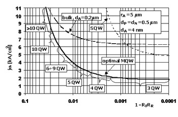
In our previous paper Reference Mackowiak and Nakwaski[48], we showed that B-VCSELs with thinner active-regions exhibit distinctly lower threshold current densities, whereas in the case of SQW VCSELs, there is an optimal active-region thickness of 40 Å. The latter result remains valid for MQW VCSELs, although there is smaller difference in the threshold current densities for different active-region thicknesses. Now let us consider the optimal number of quantum wells (M opt) for the best active-region thickness (dA = 40 Å) in GG MQW lasers. As depicted in Figure 6 for the standard set of parameters, M opt strongly depends on the reflectivities of the resonator mirrors. So, if there is a problem with manufacturing a high-reflectivity resonator mirror, it is suggested to use more than 10 quantum wells. For higher reflectivities, structures with decreasing number of quantum wells seems to be optimal. In case of IG MQW lasers, the results are similar, but for high-reflectivity resonator mirrors the optimal number of quantum wells is reduced to 2. It is also worth mentioning that threshold currents for SQW lasers in high reflectivity range are very close to threshold currents of the best MQW lasers and may be recommended as they can be produced more easily. It should be concluded as a general rule that the less that total optical losses (i.e. end losses plus internal losses) affect the laser radiation within the resonator the smaller the optimal number of QW active layers becomes (from the minimal threshold point of view). This conclusion agrees well with reported results for nitride EELs of Y. C. Yeo et al. Reference Yeo, Chong, Li and Fan[35] and discussion of D. P. Bour et al. Reference Bour, Kneissl, Romano, McCluskey, Van deWalle, Krusor, Donaldson, Walker, Dunnrowicz and Johnson[49].
Threshold current density of optimal gain-guided MQW and SQW as well as bulk VCSELs versus product of reflectivities of their resonator mirrors.
4. Conclusions
A detailed threshold analysis is carried out for nitride VCSELs to examine the usability of this semiconductor laser configuration for future mass applications. The index-guided nitride quantum-well VCSEL structure ensures the best laser performance, as expected, particularly in the case of small-size VCSELs. But surprisingly, gain-guided QW VCSELs are found to exhibit thresholds comparable to much simpler double-heterostructure VCSELs with bulk active regions.
Surprisingly, thresholds of DH nitride VCSELs are much less sensitive to all the optical losses (e.g. diffraction, scattering, absorption, and end losses) than their quantum-well counterparts. Therefore the QW VCSELs need more advanced technology (e.g. to achieve lower dislocation densities and/or higher facet reflectivities) to be superior.
The optimal number of quantum wells in both GG and IG QW VCSEL structures strongly depends on resonator mirror reflectivities and the recommended values for high-reflectivity resonator mirrors are equal to 5 and 1 respectively, whereas for low reflectivities should be more than 10. Generally, the number of quantum wells giving the best threshold performance for nitride VCSELs is proportional to the total optical losses within their resonators.
Acknowledgments
This work was supported by the Polish State Committee for Scientific Research (KBN), grant No 8-T11B-018-12.


