Introduction
Microelectronics components and systems form an ever-increasing backbone of our society. Laptops, PCs, smart phones and various forms of computing devices are indispensable for our day-to-day life. Computing devices have pervaded many parts of our daily life, for example, through a host of consumer electronics systems, providing sensing, actuation, communication, processing, and storage of information. All of these are built upon a global market that is approximately USD$420B/year and growing at a steady pace of 10–15% annually.Reference Manipatruni, Nikonov and Young1,Reference Khan, Hounshell and Fuchs2 Many of these innovations started as materials research ideas.
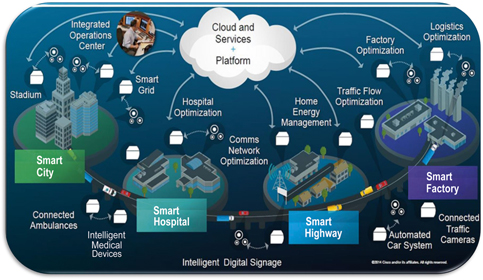
All of these will likely fade into the background by the emergence of a few global phenomena. The first is the notion of “The Internet of Things (IoT),” which is the network of physical devices, vehicles, home appliances, and other items embedded with electronics, software, sensors, actuators, and connectivity that direct integration of the physical world into computer-based systems. This will result in efficiency improvements, economic benefits, and reduced human exertion,3 as illustrated in Figure 1. It is not inconceivable that every modern building could be outfitted with millions of sensors and actuators that can dynamically optimize the energy consumption dynamics of that building. Similarly, a modern automobile has a large number of sensing and communicating components embedded.
A schematic illustrating the emergence of the “Internet of Things” and machine learning/artificial intelligence as macroscale drivers for the Beyond Moore’s Law R&D.

The second major phenomenon is the field of machine learning (ML)/artificial intelligence (AI) that is taking the technology world by storm. It uses a large amount of data, a significant amount of statistical data analytics, and provides the computing system with the ability to “learn” and do things better as it learns, much like human beings. While there are several scientific disciplines that come into play, of relevance to us is the fact that microelectronic components are critical underpinnings for this field. While still in their infancy, it is not inconceivable that driverless cars, for example, will be a routine aspect of our life 20 years from now.
How do these relate to microelectronics and, more importantly, new materials? To put this into perspective, we now need to look at the fundamental techno-economic framework that has been driving the microelectronics field for more than five decades. This is the well-known “Moore’s Law,” which underpins the field of microelectronics through the scaling of complementary metal oxide semiconductor (CMOS)-based transistors. Broadly, it states that the critical dimensions of the CMOS transistor shrink by 50% every 18–24 months. At its inception, CMOS transistors were macroscopic with critical gate dimensions well over 1 µm. In 1974, a path to shrinking them was proposed (while keeping power density constant),Reference Moore4–Reference Shannon6 and this was followed for the next 30+ years. Today, Dennard scalingReference Dennard, Rideout, Bassous and Leblanc5 is no longer possible and the critical dimensions are rapidly approaching sub-10 nm scales, at which both the fundamental science (classical electron dynamics no more suffices; quantum mechanics is needed) as well as the manufacturing issues need to be revisited. Thus, over the past five to eight years, there has been an ever-increasing sense that something has to be done about this issue.Reference Kuhn7–Reference Salahuddin and Datta11
We now introduce into this the third critical component, namely, energy consumption. Of the many issues, we focus on the energy consumed per logic operation, which in today’s CMOS transistor is on the order of 50–100 picojoules/logic operation. Let’s assume that there is no change to this number, while IoT and AI/ML start to grow as expected. It is quite conceivable that the total energy consumption of all the world’s microelectronics could grow to ∼20% of primary energy.12 Today, it is only on the order of 4% and thus is not of the greatest concern, in contrast to buildings, which require ∼38% of the total energy consumption, or transportation that takes ∼24% (in the United States). At the scale of ∼20% of primary energy, this becomes a serious component of the energy consumption mix and deserves to be addressed from the energy efficiency perspective as well. These three global phenomena, namely the emergence of IoT and AI/ML, Moore’s Law running into dimensional constraints, and the total energy consumption in microelectronics, form the backdrop for our discussion of what can be done with the fundamental science of new materials.
We can go back to the fundamentals of CMOS devices and the behavior of the electron within the CMOS transistor. The microscopic behavior of electronic charge is governed by the Boltzmann distribution.Reference Manipatruni, Nikonov and Young1,Reference Salahuddin and Datta11 A quick analysis shows that the current changes exponentially with voltage, with a slope of 60 mV/decade of current. Macroscopically, this manifests itself as an I d–V g plot with a slope of 60 mV/decade, under ideal conditions, termed as the “Boltzmann tyranny (it is a ‘tyranny’ because the Boltzmann distribution ‘imposes’ its will onto the systems behavior).”Reference Manipatruni, Nikonov and Young1,Reference Salahuddin and Datta11 In real transistors, the slope can be larger. This fundamental behavior is central to the performance of the transistor, both in terms of the voltage that is required and the energy consumed in the process of operating the transistor. In recent years, there has been the realization that the Boltzmann tyranny needs to be addressed.Reference Manipatruni, Nikonov and Young1,Reference Salahuddin and Datta11
One pathway is to use a metal–insulator–transition material, such as in correlated systems, in which electron–electron Coulombic interactions (the so-called Hubbard repulsion) or strong spin–orbit interactions lead to electronic phase transitions. Under ideal conditions, such a metal–insulator transition can be abrupt. Another key realization, which is described in a recent review,Reference Manipatruni, Nikonov and Young1 identifies the broad class of quantum materials as possible candidates to overcome this tyranny, mainly through the insertion of an additional, internal interaction energy into the Boltzmann distribution. For example, this could be the exchange interaction in a ferromagnet or the dipolar interaction in ferroelectrics. In its simplest form, such an interaction can be represented by an additional term in the Hamiltonian that represents the exchange interaction energy for a magnet (or the dipolar energy of a ferroelectric) given by the formula: E ex = –J.S1.S2, where J is the exchange integral and S1, S2 are the two neighboring spins. Depending on the sign of J, S1 and S2 are either parallel (for a ferromagnet) or antiparallel (for an antiferromagnet). This energy term then becomes the key component within the Boltzmann distribution and it modifies the energy landscape of the system. In simpler terms, the exchange energy (or the dipolar energy in a ferroelectric) makes the spins (or the dipoles) align collectively without the need for an external source of energy (such as an applied field).
Thus, if one could use the spin as the primary order parameter rather than the charge in a CMOS device, one could take advantage of such internal collective order to reduce the energy consumption. This is the premise behind two recent articles,Reference Manipatruni, Nikonov and Young1,Reference Manipatruni, Nikonov, Lin, Gosavi, Liu, Prasad, Huang, Bonturim, Ramesh and Young10 where the rudiments of a possible magnetoelectric spin–orbit (MESO) coupled memory-logic device are discussed. While many parts of this device require further detailed study and innovations, one aspect that we will focus on pertains to electric-field control of magnetism.
Electric-field control of magnetism
The first question we ask is why would one use an electric field to control magnetism, while it would be straightforward to instead use a magnetic field? One key reason is to reduce the energy consumption, perhaps by as much as a few orders of magnitude. To illustrate this, we consider two possible scenarios. The first describes how a moving electron can create a spin torque, of interest in spin transfer torque (STT)-based memory devices, Figure 2a (FM1 and FM2 are ferromagnetic layers separated by an insulating layer to form the magnetic tunnel junction). Each electron carries with it a moment of 1 Bohr-magneton that generates a large enough spin torque to move domain walls; switching magnetization requires a large number of electrons (i.e., a large current), which, in turn, requires an appropriate current source (i.e., a battery). For nominal dimensions (e.g., 10 nm × 10 nm lateral dimensions) one can estimate the energy consumed in this process, which is on the order of a few femtoJoules (Figure 2a). One can contrast this to a capacitive device, with an electric field modulating the charge. Depending upon the dielectric permittivity, one can generate relatively large fields on the order of 10 kV/cm in the dielectric (Figure 2b). In turn, the energy required to manipulate a 10 nm × 10 nm capacitor with a dielectric constant of ∼100 can be on the order of 1 attoJoule.
A set of schematics illustrating the energy consumption for nominal devices. (a) Current-driven spin-torque switching device. Each electron can transfer only 1 µB, intrinsically requiring large currents and charge. (b) Voltage-driven magnetoelectric switch. Each charge can generate a field of e/(ε.A) intrinsically requiring small amount of charge for high fields. Note: FM, ferromagnet; ME, magnetoelectric.

We now consider the prospects and progress in electric-field control of magnetism. We focus on the use of multiferroics and magnetoelectrics as the pathway. With the pace of this field and its breadth, it will be impossible to cover all of the developments within this article. Therefore, we direct the reader toward two recent reviewsReference Song, Cui, Li, Zhou and Pan13,Reference Spaldin and Ramesh14 of this subject for in-depth information on various pathways.
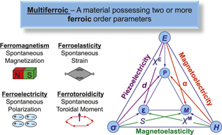
First, it seems pertinent to describe the symmetry basis for multiferroics and magnetoelectrics, as shown in Figure 3. Magnetism breaks time-reversal symmetry. The key symmetry-breaking attribute of a magnet is that reversal of the current direction (equivalent to reversing time) leads to a reversal of the magnetic field direction. A ferroelectric, on the other hand, breaks spatial inversion symmetry (e.g., a mirror plane is lost during the phase transition). In contrast to these two, a ferroelastic (such as martensite) breaks neither time nor spatial inversion symmetry. The apparent lack of a fourth component to complete this picture was recognized in the early years of multiferroics research,Reference Ederer and Spaldin15 leading to the addition of a fourth-order parameter, namely, a ferrotoroidic order (i.e., one that breaks both time and spatial inversion symmetry).
A schematic illustrating the four fundamental symmetry-based order parameters in solids. On the right is the classic “Nye-diagram” showing the coupling between the intrinsic and extrinsic thermodynamic variables.

With this fundamental symmetry insight, we now ask how does one couple magnetism to an electric field such that the state and direction of magnetism can be manipulated through the application of an electric field? In nature, this coupling between electricity and magnetism occurs through electromagnetism. However, in order to be able to dramatically change the state of magnetism with an electric field, it is desirable for the magnetoelectric coupling to be significantly stronger than what is available in nature. A few solid-state materials exhibit the coexistence of magnetism of some form (typically antiferromagnetism or a canted derivative) with ferroelectricity and they are called multiferroics; if there is coupling between these orders, they are also magnetoelectric. Unfortunately, the fundamental requirements for the existence of ferromagnetism, most notably, the need for exchange interactions (i.e., electrons have to move around) to establish a ferromagnetic state, is in direct conflict with the requirements for a polar-ordered state (such as ferroelectricity) that requires the material to be an insulator. This contradicting set of requirements is perhaps the biggest challenge and requires some clever materials design.Reference Spaldin and Ramesh14
Among the handful of known multiferroics, bismuth ferrite is one of the most studied systems because (1) it is one of the earliest identified “correlated electron” systems (similar to the manganites and more recently the iridates), that is, without introducing electron–electron correlations, the material is essentially a weak semiconductor with a small bandgap;Reference Ederer and Spaldin16 introduction of correlations opens up a gap of about 2.7 eV and thus the insulating behavior; (2) it has robust magnetic and ferroelectric ordering at room temperature; (3) although it does not show a linear magnetoelectric coupling in the bulk due to the existence of a spin spiral, it does show a linear magnetoelectric coupling in thin films, since the spiral is typically broken; and (4) it exhibits a large number of physical phenomena, as shown in Figure 4, within the same material as well as the existence of multiple crystal phases as a function of chemistry and constraints (mainly elastic constraints imposed due to epitaxial strain), as described in Figure 5, all of which exhibit different magnetic and ferroelectric responses. While the intention of this article is not to just focus on this material system, we will use it to illustrate the richness of the materials physics available as well as illustrate some possible applications, with a strong focus on electric-field control of magnetism. A recent review gives a broader perspective on the entire range of multiferroics and magnetoelectrics.Reference Spaldin and Ramesh14
(a) Polarization-voltage loops for various orientations of the model multiferroic, BiFeO3 (BFO); (b) THz response loops for BiFeO3; (c) large photostriction in BiFeO3 crystals; and (d) large photochromic effects in Ca-BiFeO3.

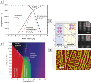
Phase stability in BiFeO3 (BFO). (a) A phase-field calculation showing the effects of epitaxial strain on the phase stability; (b) the effects of Ca-doping in BFO on the chemical phase stability; (c) and the top panel shows ab initio calculations of the effects of in-plane compression on the phase stability; on the right are atomic resolution images of the R-phase and the super-tetragonal, T-phase; (d) on the bottom is an atomic force microscope image of the mixed, R/T phases in epitaxial thin films.Reference Zeches, Rossell, Zhang, Hatt, He, Yang, Kumar, Wang, Melville, Adamo, Sheng, Chu, Ihlefeld, Erni, Ederer, Gopalan, Chen, Schlom, Spaldin, Martin and Ramesh24

The initial focus was on validating the large value of spontaneous polarization in this system. In the early days of this field, this by itself was controversial and was intensely debated, since prior work on bulk ceramics had yielded a polarization value of ∼6 µC/cm2.Reference Spaldin and Ramesh14 It is now clear that these low values were a consequence of either electrical leakage or due to impure materials. Epitaxial thin films in controlled orientations (100, 110, and 111) yield the true value of spontaneous polarization (∼90 µC/cm2, consistent with ab initio theoretical calculationsReference Ederer and Spaldin16) (Figure 4a). Subsequent work over the past decade has demonstrated a plethora of physical phenomena, including a strong THz radiationReference Takahashi, Kida and Tonouchi17 (Figure 4b), large photostrictionReference Kundys, Viret, Colson and Kundys18 (Figure 4c), and large electrochromic effects in Ca-doped BiFeO3 filmsReference Seidel, Luo, Suresha, Nguyen, Lee, Kim, Yang, Pennycook, Pantelides, Scott and Ramesh19 (Figure 4d). Ferroelectric domain walls in this system are also quite rich in their physical responses.Reference Catalan, Seidel, Ramesh and Scott20,Reference He, Yeh, Yang, Singh-Bhalla, Liang, Chiu, Catalan, Martin, Chu, Scott and Ramesh21 Early work showed the possibility for electrical conduction at specific types of domain walls, which were also spin-polarized and showed large magnetoresistance values. This work has led to a new area of research within the field of complex correlated oxides, which is focused on exploring transport at domain wallsReference Meier22 and the possibility of exotic phenomena, such as an insulator–metal transition right at the domain wall. Large photovoltaic responses were also observed in films with arrays of domain walls.Reference Yang, Seidel, Byrnes, Shafer, Yang, Rossell, Yu, Chu, Scott, Ager, Martin and Ramesh23
The second unique feature of this system has been the fact that it is structurally “malleable,” not in the sense of a conventional metal, but from the fact that the parent rhombohedral structure can be systematically morphed into other symmetries using epitaxy as a constraint. This is illustrated in Figure 5. Under compression, the rhombohedral ground state undergoes an isosymmetric phase transition to a tetragonal structure (both of them are monoclinically distorted symmetries).Reference Zeches, Rossell, Zhang, Hatt, He, Yang, Kumar, Wang, Melville, Adamo, Sheng, Chu, Ihlefeld, Erni, Ederer, Gopalan, Chen, Schlom, Spaldin, Martin and Ramesh24,Reference Bea, Dupe, Fusil, Mattana, Jacquet, Warot-Fonrose, Wilhelm, Rogalev, Petit, Cros, Anane, Petroff, Bouzehouane, Geneste, Dkhil, Lisenkov, Ponomareva, Bellaiche, Bibes and Barthélémy25 This super-tetragonal phase embodies an even larger polarization of ∼150 µC/cm2. If the epitaxial strain is partially relaxed (e.g., thickening the film), the system goes into a nanoscale (∼20–30 nm) ensemble of the two phases, with a coherent interface separating them. The rhombohedral phase in this ensemble is highly distorted and shows a strongly enhanced canted moment compared to the bulk.Reference He, Chu, Heron, Yang, Liang, Kuo, Lin, Yu, Liang, Zeches, Kuo, Juang, Chen, Arenholz, Scholl and Ramesh26 These two phases can be reversibly switched with an electric field. In contrast, if we impose a tensile strain on the parent phase, an orthorhombic symmetry can be stabilized. Not much is known about the polarization and magnetic properties of this symmetry. Chemical substitutions at the Bi-site or Fe-site can also be used to create phase changes as well as phase mixtures.
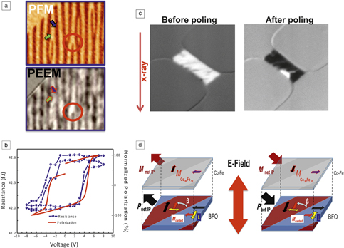
Unlike, ferromagnetism, for which macroscopic magnetic measurements (such as SQUID magnetometry, magnetooptic Kerr measurements, or x-ray magnetic circular dichroism measurements) are possible, probing antiferromagnetic order is not straightforward since there is no macroscopic magnetic moment. Instead, one has to resort to neutron scattering or x-ray optical studies to probe the antiferromagnetic order. Electric-field control of antiferromagnetism requires probing the magnetism using x-rays or neutrons. Using both for studies of BiFeO3 (BFO) has shown that when the polarization state switches with the application of an electric field, the corresponding magnetic order also rotates by a commensurate angle.Reference Zhao, Scholl, Zavaliche, Lee, Barry, Doran, Cruz, Chu, Ederer, Spaldin, Das, Kim, Baek, Eom and Ramesh27,Reference Lebeugle, Colson, Forget, Viret, Bataille and Gukasov28 Such a change can also be probed with spatial resolution using a combination of piezoforce microscopy (to image the ferroelectric order) and x-ray linear dichroism-based photoemission electron microscopy (to image the antiferromagnetic order) (Figure 6). It is interesting to note that there has been little detailed work on a full understanding of how the antiferromagnetic state is manipulated by an electric field. This is particularly surprising, since the antiferromagnetic resonance frequencies are in the several hundred GHz range and BFO has coupled spin-charge waves (also known as ferroelectromagnons) in the 700 GHz range. Given the current surge in interest in antiferromagnetic spintronics, we expect that such insulating multiferroics that exhibit electrical-field controllable antiferromagnetism would also garner more interest, specifically from the high-frequency community.
Electric-field control of antiferromagnetism probed using x-ray linear dichroism-based photoemission electron microscopy (XLD-PEEM). (a) Piezoforce microscopy showing the ferreoelectric domain structure before switching; the corresponding XLD-PEEM image (illustrating the antiferromagnetism) is shown at the left bottom. The corresponding polarization force microscopy (PFM)/PEEM images after switching are shown in (b).Reference Zhao, Scholl, Zavaliche, Lee, Barry, Doran, Cruz, Chu, Ederer, Spaldin, Das, Kim, Baek, Eom and Ramesh27

We now turn to the central question, can we control the magnetic state or magnetization direction with an electric field? Over the past four years, both of these have been proven to be possible, as illustrated in Figure 7.Reference Heron, Bosse, He, Gao, Trassin, Ye, Clarkson, Wang, Liu, Salahuddin, Ralph, Schlom, Íñiguez, Huey and Ramesh29–Reference Lee, Liu, Heron, Clarkson, Hong, Ko, Biegalski, Aschauer, Hsu, Nowakowski, Wu, Christen, Salahuddin, Bokor, Spaldin, Schlom and Ramesh32 There have been several manifestations of this idea, which are well discussed in recent reviews.Reference Song, Cui, Li, Zhou and Pan13,Reference Spaldin and Ramesh14 Furthermore, recent workReference Manipatruni, Nikonov, Lin, Gosavi, Liu, Prasad, Huang, Bonturim, Ramesh and Young10 has demonstrated that voltage control of magnetism can be driven down to less than 1 V, with the potential to go down to even lower voltages through thickness reductions and chemical substitutions.
(a) The top image is a piezoforce microscope image of the ferroelectric domain structure in the BiFeO3 (BFO) layer; the bottom image is the x-ray magnetic circular dichroism-photoemission electron microscope (XMCD-PEEM) image of the CoFe layer that is deposited on this illustrating that the ferromagnetic CoFe couples to the BFO layer; (b) is a plot of the CoFe-Cu-CoFe spin-valve resistance as a function of applied voltage (in blue) while the corresponding ferroelectric switching data are in red; (c) is a set of XMCD-PEEM images at the Co-edge showing a reversal of contrast after an electrical switching event; (d) shows a schematic of what happens to the canted moment in the BFO and the CoFe moment before and after the electrical switching.Reference Heron, Bosse, He, Gao, Trassin, Ye, Clarkson, Wang, Liu, Salahuddin, Ralph, Schlom, Íñiguez, Huey and Ramesh29 Note: PFM, polarization force microscopy.

It seems inappropriate to write a concluding section, when in reality, the exciting journey has just begun. Electric-field control of the magnetization direction at room temperature is now clear, with the voltage required to accomplish this dropping down to 0.5 V. To get to an attoJoule switch, it is critical to drop these switching voltages down even further, to about 100 mV, in conjunction with a switching charge density of ∼10 μC/cm2.Reference Manipatruni, Nikonov, Lin, Gosavi, Liu, Prasad, Huang, Bonturim, Ramesh and Young10 How robust can this be, especially with respect to repeated cycling of the electric and magnetic states? In this regard, such as in the field of ferroelectric thin films for memory applications, it appears that we need to start to focus on the nature of the ferromagnet and its interface to the multiferroic. Prior experience with ferroelectric capacitors has shown that a conducting oxide contact yields a robust capacitor; in a similar vein, we expect an oxide ferromagnet to form a more robust contact to the multiferroic. Thus, there is an urgent need to discover and interface an oxide ferromagnet that couples magnetically to the multiferroic at room temperature. A template for this is already available from the work on La-Sr-Mn-O3–Bi-Fe-O3 interfaces,Reference Wu, Cybart, Yu, Rossell, Zhang, Ramesh and Dynes33 which display robust electric-field control of the magnetization direction, albeit at 100 K.
In the same vein, there is an urgent need to discover more room-temperature multiferroics so that one can explore multiple pathways to use these novel functionalities. Finally, we believe that exploring for new room-temperature multiferroics would be a worthwhile pursuit for the materials community, especially when armed with computational discovery platforms such as the Materials Project and the Materials Genomics approach driven by ML pathways.
Acknowledgments
We thank the Kavli Foundation for endowing this lectureship. Their support of fundamental science worldwide is greatly appreciated. We have written this article on behalf of a large number of collaborators and co-workers worldwide and acknowledge the intellectual participation and contribution of a large number of our colleagues worldwide. Our work would not have been possible without the sustained support of federal and industrial funding agencies. Particularly, we gratefully acknowledge the sustained support of the US Department of Energy Basic Energy Sciences Office, the National Science Foundation’s MRSEC program, the Semiconductor Research Corporation’s JUMP Initiative, and the DOD MURI programs that have supported this work over several years.

Ramamoorthy Ramesh is the Purnendu Chatterjee Chair Professor in Materials Science and Physics at the Lawrence Berkeley National Laboratory. From 2010 to 2012, he served as the founding director of the SunShot Initiative at the US Department of Energy. In 2011, he was elected to the National Academy of Engineering. His current research focuses on key scientific and technological problems in complex multifunctional oxide thin films, nanostructures, and heterostructures. He has more than 65,000 citations and an H-factor of 110. He is a Fellow of the American Physical Society (APS), AAAS, and the Materials Research Society. His numerous awards include a Humboldt Senior Scientist Prize, the APS David Adler Lectureship and the James McGroddy Prize, and the 2018 IUPAP Magnetism Prize and Neel Medal. Ramesh can be reached by email at rramesh@berkeley.edu.

Sasikanth Manipatruni is the founding research director of the Intel Corporation Functional Electronics Integration and Manufacturing Center, and also senior counsel to the CTO of the Intel AI group. He received his PhD degree from Cornell University in silicon photonics. His current research focuses on building the next room-temperature transistor with quantum materials. He was awarded the IEEE/ACM Under 40 Innovator Award in 2017, Mahboob Khan Outstanding Liaison Award in 2016, and the CSPIN Outstanding Industry Liaison Award in 2016. His work has been cited approximately 3600 times and he holds approximately 200 granted/applied patents in spin/photonics/MEMS/CAD/AI/QC. Manipatruni can be reached by email at sasikanth.manipatruni@intel.com.

Ian Young is a senior Fellow and director of Exploratory Integrated Circuits in the Technology and Manufacturing Group of Intel Corporation. He received his bachelor’s degree in electrical engineering and his MS degree in engineering science from The University of Melbourne, Australia. He received his PhD degree in electrical engineering from the University of California, Berkeley. His current research explores the future options for the integrated circuit in the beyond complementary metal oxide semiconductor era. He is the recipient of the 2009 International Solid-State Circuits Conference’s Jack Raper Award for Outstanding Technology Directions paper. He received the 2018 IEEE Frederik Philips Award and is a Fellow of the IEEE. Young can be reached by email at ian.young@intel.com.