

I. INTRODUCTION
Magnetic-resonant wireless power transfer (MRWPT) has been realized by Karalis et al. in 2007 in [Reference Kurs, Karalis, Moffatt, Joannopoulos, Fisher and Soljacic1] and he has generated a significant interest among researchers. In [Reference Kurs, Karalis, Moffatt, Joannopoulos, Fisher and Soljacic1], the experimental realization has been made by using two self-resonant coils. One coil (the source coil) has been inductively coupled to an oscillating circuit operating at a frequency of 9.9 MHz the other (the device coil) has been inductively coupled to a resistive load. Self-resonant coils relied on the interplay between distributed inductance and distributed capacitance to achieve resonance. The coils were made of an electrically conducting wire of total length l and cross-sectional radius a wound into a helix of n turns, radius r, and height h; the values chosen for the experiment have been: h = 20 cm, a = 3 mm, r = 30 cm, and n = 5.25. The driving circuit has been excited by means of a Colpitts oscillator in which the inductance has been made with a copper loop of radius 25 cm. As an example, when transferring 60 W to the load over a distance of 2 m the power flowing into the driving circuit was 400 W. This has provided an overall DC/DC efficiency of 15%, which has been considered reasonable given the expected efficiency of 40–50% for the wireless power transfer at that distance and the low efficiency of the Colpitts oscillator.
In [Reference Kurs, Karalis, Moffatt, Joannopoulos, Fisher and Soljacic1, Reference Karalis, Joannopoulos and Soljačić2], coupled mode theory was used for the analysis; successively a network approach, more suitable for engineering purposes, has been introduced in [Reference Zhu, Yu, Liu and Ma3]. In [Reference Si, Hu, Malpas and Budgett4], a method has been presented to regulate the power transferred over a wireless link by adjusting the resonant operating frequency of the primary converter. With this approach, effective power regulation is maintained under variations in load, coupling, and circuit parameters. This is particularly important when the wireless supply is used to power implanted medical devices where substantial coupling variations between internal and external systems is expected. The operating frequency is changed dynamically by altering the effective tuning capacitance through soft switched phase control. However, this method requires a bidirectional communication link.
The feasibility of MRWPT for electrical vehicles (EVs) has been considered in [Reference Imura, Okabe and Hori5], and efficiencies of approximately 95–97% have been reported for the wireless channel. In this study, the resonators have been called antennas; however the resonators are expected to couple to each other (via magnetic fields) but should not radiate energy into the environment. Also in this case series resonators have been used.
In [Reference Low, Chinga, Tseng and Lin6], a design approach has been proposed in order to realize an efficient wireless power transfer system achieving low-power loss using the class-E mode of operation. In this excellent work, an inductive coupling has been considered and impedance transformation networks have been added. Four topologies (combination of series and parallel) for a single element impedance have been considered, but no systematic design procedure has been introduced. However, the proposed system has been able to achieve a desirable power-delivery response across a wide range of load resistances without any control mechanism or feedback loop. An efficient compact wireless power system achieving 295 W of power delivery with better than 75% end-to-end dc-to-dc conversion efficiency across the main power-delivery impedance range has been achieved. The selected operating frequency has been 134 kHz and purely circuital models have been used. Subsequently, a load detection scheme without using any communication link between the transmitting platform and the receiving unit has been proposed and implemented in a wireless power transfer system in [Reference Low, Casanova, Maier, Taylor, Chinga and Lin7]. By using the transmitter coil voltage and supply current space, it has been shown that the system is capable of differentiating among a safe zone for nominal operation, no-load zone for energy saving, and fault zone when invalid loads that might damage the system are present. In this work a class-E transmitter operating at 240 kHz has been considered.
A MRWPT system and a suitable tuning method have been presented in [Reference Chen, Chu, Lin and Jou8] using loosely coupled coils. The MRWPT system has been implemented with two coupled resonators consisting of lumped coils and high-Q variable capacitors. Compared to the distributed resonators of the original experiment in [Reference Kurs, Karalis, Moffatt, Joannopoulos, Fisher and Soljacic1], the system proposed in [Reference Chen, Chu, Lin and Jou8] might be dynamically tuned for different operating distances. According to the authors, the natural frequencies need to be slightly displaced from each other in order to avoid the power transfer bifurcation phenomenon. Also in this case no systematic design procedure has been given in order to realize the entire wireless channel.
MRWPT has been experimentally demonstrated in a system with a large source coil and either one or two small receivers in [Reference Cannon, Hoburg, Stancil and Goldstein9]; in this work resonance between source and load coils has been achieved with lumped capacitors terminating the coils. Resonant frequency splitting has been observed experimentally and described theoretically for the multiple receiver system. The authors also stated that, in a multiple receiver system, a means for tracking frequency shifts and continuously retuning the lumped capacitances that terminate each receiver coil so as to maximize efficiency should be a key issue for the future work.
In MRWPT, we can distinguish four different cases, depending whether the frequency is fixed or allowed to change and whether the coupling is fixed or variable. In [Reference Mastri, Costanzo, Dionigi and Mongiardo10–Reference Costanzo, Dionigi, Mastri and Mongiardo12], the authors have considered a case in which the coupling and the frequency are both allowed to change. This has been realized by using a Royer oscillator, which changes its frequency depending on the load. A case in which the coupling has been considered fixed has been described, e.g. in [Reference Lee and Lorenz13] where the authors have achieved a 95% efficiency 220-W wireless power transfer over a 30-cm air gap. The frequency selected by the authors has been 3.6 MHz. The high efficiency has been reached by tuning of the network elements; the load has been selected with an optimized value. However, the lack of a rigorous, systematic, approach makes each design a special case.
An excellent investigation of the underlying principles of coupled magnetic resonance, as well as a simple circuit model of the system has been provided in [Reference Sample, Meyer and Smith14]. It has been shown that frequency splitting, operating range, and impedance matching play a critical role. In addition, in order to accurately characterize the wireless power system, measurement techniques that use a network analyzer for circuit parameter extraction have been implemented.
In the works of [Reference Lee and Nam15, Reference Yuan, Chen, Li and Sawaya16] also radiation aspects have been considered; in [Reference Dionigi, Franceschetti and Mongiardo17] it has been shown that, when multiple resonances are present, it is possible that radiation occurs at one of the resonances. It is therefore of importance to take into account also possible radiative effects.
A rather comprehensive review work on the theory and techniques for MRWPT has been presented in the chapters [Reference Dionigi, Costanzo and Mongiardo18, Reference Dionigi, Costanzo, Mastri and Mongiardo19] and the relative books also provide a good overview of the approaches employed so far.
In [Reference Dionigi and Mongiardo20], the computer aided design of wireless power transfer systems has been investigated. Efficiency investigations have been presented in [Reference Dionigi and Mongiardo21, Reference Dionigi and Mongiardo22], together with appropriate network representations [Reference Dionigi and Mongiardo23] also making use of immittance inverters. We will see in this work that, by using immittance inverters, it is possible to design a network, which models the entire wireless channel, in a rigorous way.
So far, MRWPT systems have been realized by using coupled resonators. This approach may lead to good results but does not explicitly show how to design an efficient MRWPT system. We will start, instead, by considering just the coupled inductances and then adding elements (either capacitive or inductive) in order to realize a particular network. In the next sections, we separate the MRPWT problem into different parts and we introduce a novel way to look at the wireless channel. It will be shown that it is possible to design in a systematic way, at a single frequency, a network that allows to efficiently transmit power to a remote load.
The proposed technique significantly extends the range of applications. As an example, it can be applied in conjunction with self-oscillating switched power converter, as the one proposed in [Reference Zhao, Yu, Leng and Chen24]; this converter employs two unique switched impedance networks to couple the main circuit and the power source and load. Another possible application is the one suggested in [Reference Russer and Russer25], where EVs are charged with a moving field wireless power transfer system.
II. GENERAL DESCRIPTION OF A MRWPT SYSTEM
A convenient general description of an MRWPT system consists (see Fig. 1) of the following three parts:
i) a transmitting circuit which performs a power conversion from P DC,in to P RF,1;
ii) the wireless channel, which can be seen as a passive two-port network, that transfers the power P RF,1 impinging in port 1 to the power P RF,2 outgoing from port 2;
iii) a receiving circuit which performs a power conversion from P RF,2 to P DC,out.
The challenging part is the realization of the wireless channel: this is a two-port network but with the circuitry associated to port 1 physically separated from the circuitry associated to port 2. Ideally, this two port network should represent at port 1 the load attached at port 2, therefore it should behave as an ideal transformer. Since port 1 and port 2 are not physically connected, we may call this component as a wireless transformer. A possible network implementation of this component is described in the next section.
Block representation of an MRWPT system; the wireless channel is typically obtained by considering inductors coupled via their resonant magnetic fields.

III. THE 1:n WIRELESS TRANSFORMER
The MRWPT system performs essentially a DC–DC conversion between a primary side and a secondary side which are physically at a distance in space. The energy coupling between the primary (transmitting) side and secondary (receiving) side is realized by the magnetic field. In this arrangement, we can have currents on an inductor L 1 on the primary side; a part of the magnetic field generated by these currents can couple to another inductor L 2 present on the secondary side. The network elements that represent the aforementioned coupling mechanism are the mutually coupled inductances, which have the following impedance representation:
 $$Z = \left[{\matrix{ {j\omega L_1 } & {j\omega M} \cr {j\omega M} & {j\omega L_2 } \cr } } \right]$$
with the mutual inductance M being defined as  $M = k\sqrt {L_1\, L_2 } $ and k being the coupling coefficient.
By using a suitable network representation of the coupled inductances, we can realize, at a selected frequency, a wireless, i.e. with the primary side separated from the secondary side, 1:n transformer.
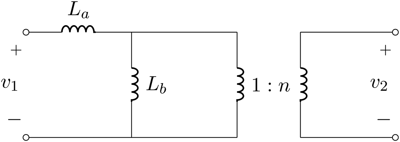
Let us consider the representation of the mutually coupled inductances illustrated in Fig. 2; we note the following equivalences:
 $$\eqalign {L_a & = \lpar 1 - k^2 \rpar L_1\comma \; \cr L_b & = k^2\, L_1\comma \; \cr n & = \displaystyle{1 \over k}\sqrt {\displaystyle{{L_2 } \over {L_1 }}}.}$$
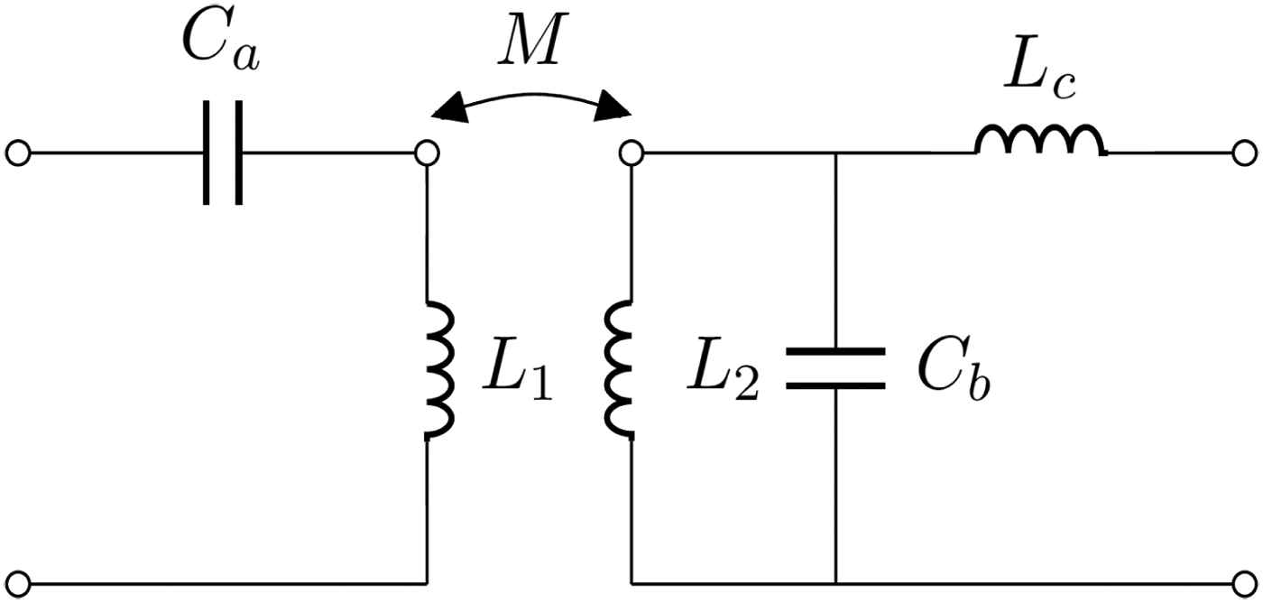
From Fig. 2, we can see that it is possible to obtain a 1:n transformer at ω = ω 0 by compensating the inductances L a and L b. As a first step, we can compensate L b by adding a shunt capacitance C b on the secondary side, as shown in Fig. 3. If this capacitance is reported on the primary side its value becomes n 2C b. Hence, by looking at the parallel circuit composed by L b and C bn 2, we can impose that its admittance vanishes at the frequency ω 0, thus providing an open circuit. The latter condition is realized when:
 $$C_b = \displaystyle{1 \over {\omega _0^2 }}\displaystyle{1 \over {n^2\, L_b }} = \displaystyle{1 \over {\omega _0^2 }}\displaystyle{1 \over {L_2 }}.$$
In order to compensate the inductance L a we may start by adding a series inductance L c on the secondary side (see Fig. 3). When reported on the primary side this inductance becomes L c/n 2. It is thus possible to compensate the −k 2L 1 part of L a; by letting:
 $$L_c = n^2\, k^2\, L_1 = L_2 .$$
Finally, we add the series capacitance C a on the primary side and we chose its value in order that the series of C a and L 1 presents zero impedance at ω 0. By so doing we recover:
 $$C_a = \displaystyle{1 \over {\omega _0^2 }}\displaystyle{1 \over {L_1 }}.$$
By choosing the values of C a, C b, and L c as indicated in equations (5), (3), and (4), respectively, we have realized at ω = ω 0 a 1:n wireless transformer.
Representation of coupled inductances in terms of a series inductance L a, a shunt inductance L b and a 1:n ideal transformer.
In this figure L 1 and L 2 are the inductances of the primary and secondary side, respectively; M is their mutual inductance. A series capacitance C a has been added on the primary side; a parallel capacitance C b has been added on the secondary side and, finally, a series inductance L c has been added on the secondary side. The above network realizes at ω = ω 0 a wireless 1:n transformer.
In conclusion, the design procedure goes as follows: we set appropriate values for L 1, L 2, and k (the problem under examination with its specific constraints provides these values). The designer selects an operating frequency ω 0. A series capacitance C a, with value indicated by equation (5), is added on the primary side. A parallel capacitance C b, with value indicated by equation (3), is added on the secondary side. A further series inductance L c, with value given in (4), is placed on the secondary side. The above procedure solves the problem of transferring energy in wireless manner to a load physically separated from the source.
Note that the values of C a, C b, and L c do not depend on the coupling k, which only affects the transformer ratio, according to (2). Hence, in order to obtain the same transformer ratio n for different values of the coupling k, it is sufficient to add, either at port 1 or at port 2, a standard transformer of appropriate ratio. When changing the coupling k, we need only to adjust the standard transformer ratio.
It is also interesting to observe that the series resonant circuit composed by C a and L 1 and the parallel resonant circuit composed by C b and L 2 are synchronous; however, it is the presence of L c, which allows to realize at ω 0 a 1:n wireless transformer.
The proposed approach provides a network that solves the problem of transferring power to a physically remote load. However, the above considered 1:n wireless transformer is just a special case of a more general network in which the coupled inductances are realized by means of immittance inverters, as will be discussed in the next section.
IV. REPRESENTATIONS USING IMMITTANCE INVERTERS
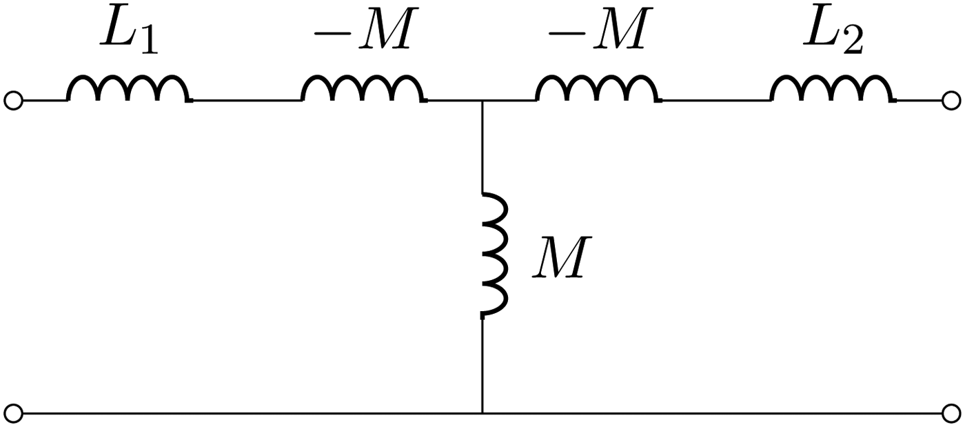
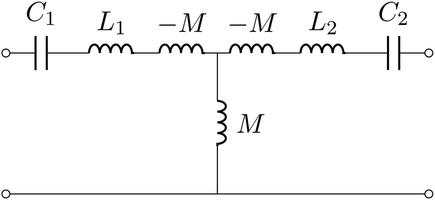
Another network representation for coupled inductances is shown in Fig. 4; the central part, with the series inductors −M and the parallel inductor M, realizes, at given frequency, an immittance inverter with the following ABCD matrix:
 $$\left[{\matrix{ A \hfill& B \cr C \hfill& D \cr } } \right] = \left[{\matrix{ 0 \hfill& { - j\omega M} \cr {\displaystyle{{ - j} \over {\omega M}}} \hfill& 0 \cr } } \right].$$
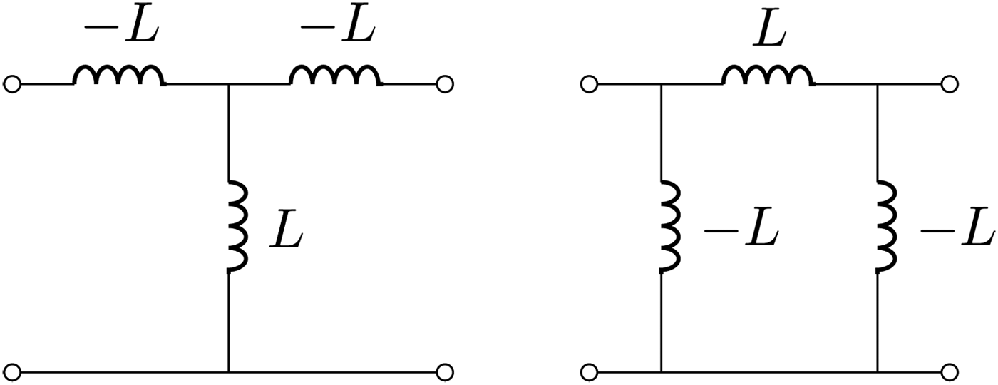
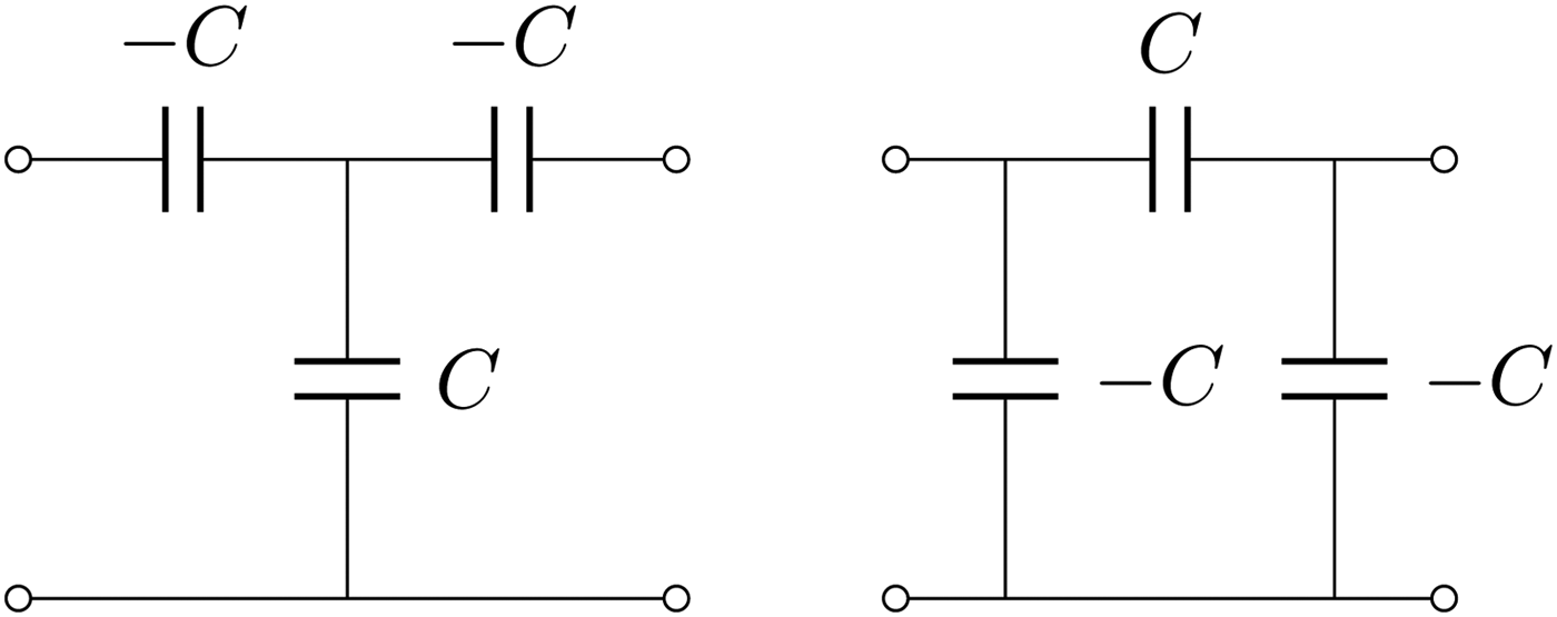
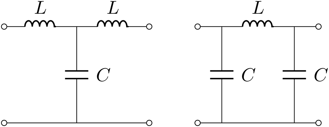
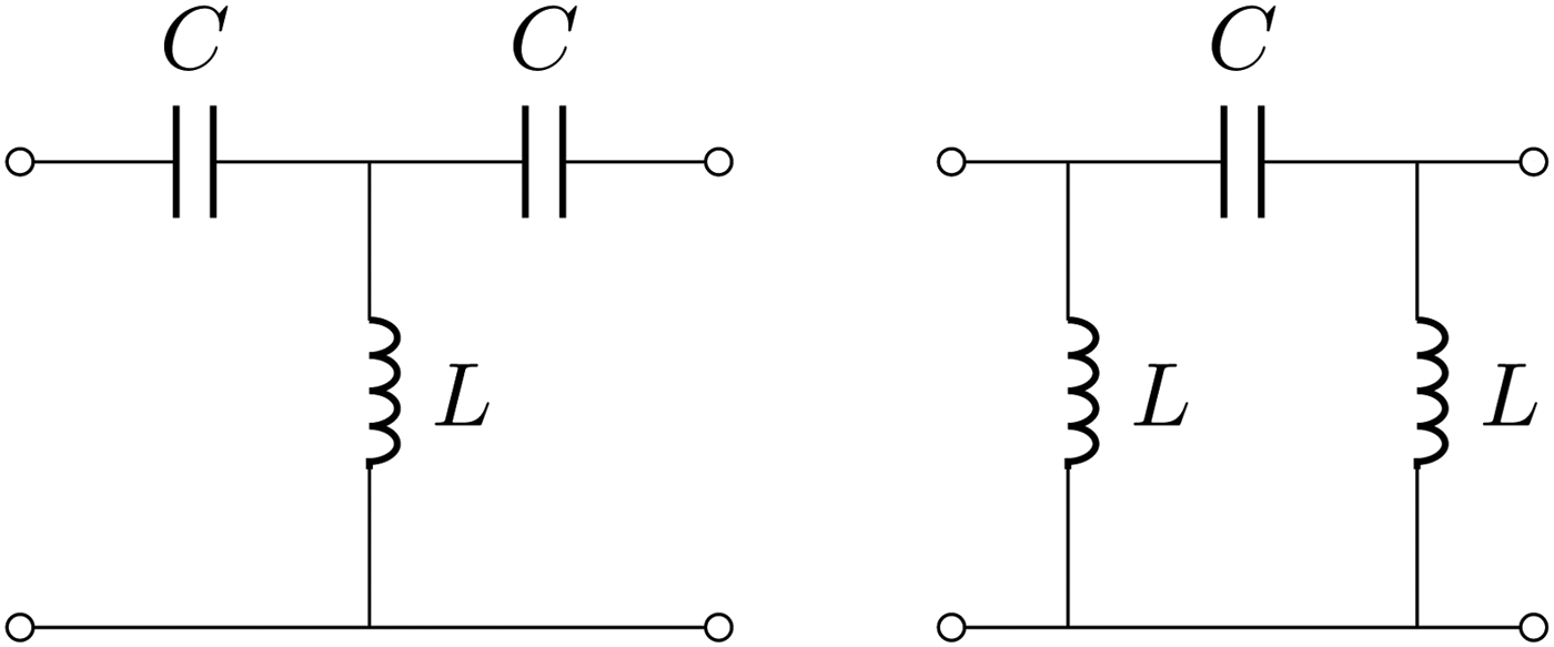
We can denote the latter immittance inverter of value −ωM with Tee(−M, M, −M). It is also possible that a Pi network with values Pi(−M, M, −M) realizes an immittance inverter of value ωM as shown in Fig. 5. Immittance inverters can also be realized with capacitive networks as shown in Fig. 6.
Coupled inductances equivalent network: T representation. The central part, with the series inductors −M and the parallel inductor M, realizes an immittance inverter.
Inductive immittance inverters: the Tee representation is shown on the left side and provides an inverter value of −ω 0L. On the right side is shown a Pi network with values Pi(−L, L, −L) which realizes an immittance inverter of value ω 0L.
Capacitive immittance inverters: the Tee representation is shown on the left side and provides an inverter value of 1/ω 0C. On the right side is shown a Pi network with values Pi(−C, C, −C) which realizes an immittance inverter of value −1/ω 0C.
Let us select an operating frequency denoted by ω 0; we consider, in the following, circuits composed by L and C that satisfy the relation:
 $$C = \displaystyle{1 \over {\omega _0^2 }}\displaystyle{1 \over L}.$$
The series LC at resonance realizes a short circuit, whereas the parallel LC at resonance is an open circuit. It is therefore possible to derive the equivalences shown in Figs 7 and 8. By adding capacitances to the coupled inductance network we can recover several interesting cases.
LC immittance inverters: the Tee(L, C, L) representation is shown on the left side and provides an inverter value of ω 0L, when equation (7) is satisfied. On the right side is shown a Pi network with values Pi(C, L, C), which realizes an immittance inverter of value ω 0L.
LC immittance inverters: the Tee(C, L, C) representation is shown on the left side and provides an inverter value of −ω 0L, when equation (7) is satisfied. On the right side is shown a Pi network with values Pi(L, C, L) which realizes an immittance inverter of value −ω 0L.
A) Adding series–series capacitances
With reference to Fig. 4, we can add a series capacitance C 1 on the primary side and a capacitance C 2 on the secondary side. By selecting the value of C 1 such that:
 $$C_1 = \displaystyle{1 \over {\omega _0^2 }}\displaystyle{1 \over {L_1 }}\comma \;$$
and the value of C 2 such that:
 $$C_2 = \displaystyle{1 \over {\omega _0^2 }}\displaystyle{1 \over {L_2 }}\comma \;$$
we have that, at ω = ω 0, the series of L 1, C 1 and L 2, C 2 realizes a short circuit. As a consequence, the entire network of Fig. 9 behaves as a single impedance inverter. We can now realize, e.g. a 1:1 wireless transformer by adding another equal impedance inverter either on the primary or on the secondary side. While the values of C 1 and C 2 do not depend on the coupling k, the value of the impedance inverter depends on k.
Coupled inductances equivalent network with added capacitances C 1 and C 2. At a selected frequency ω = ω 0, the series of L 1, C 1 and L 2, C 2 realize a short circuit and the entire network behaves as an impedance inverter.
B) Adding series–parallel capacitances
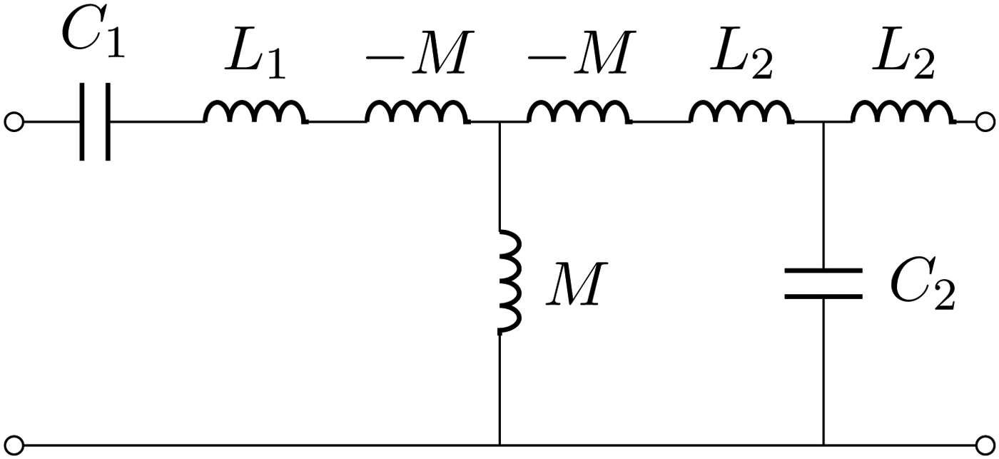
Another possibility is to add a series capacitance C 1 on port 1 and a parallel capacitance C 2 on port 2 as shown in Fig. 10. Further addition at port 2 of a series inductor creates the Tee(L 2, C 2, L 2) which represents another immittance inverter. Thus, at a selected frequency ω = ω 0, the entire network behaves as two cascaded immittance inverters. Since two cascaded immittance inverters realize a transformer, this network is the same realized in Section III and therefore implements a 1:n transformer.
A series capacitances C 1 and a parallel capacitance C 2 have been added respectively on port 1 and port 2. Further addition at port 2 of a series inductor results in the structure shown in the figure. Note that at port 2 the Tee(L 2, C 2, L 2) represents another impedance inverter. Thus, at a selected frequency ω = ω 0, the entire network behaves as two cascaded immittance inverters.
C) Adding parallel–parallel capacitances
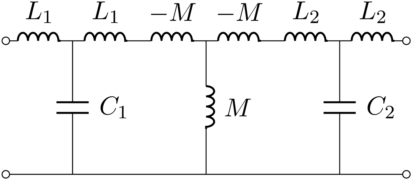
By adding parallel capacitors C 1, C 2 and series inductors L 1, L 2, we obtain the structure of Fig. 11. It is noted that this network is the cascade of three immittance inverters.
A parallel capacitances C 1 and a parallel capacitance C 2 have been added respectively on ports 1 and 2. Further addition at ports 1 and 2 of the series inductors L 1, L 2, results in the structure shown in the figure. Note that at port 1 the Tee(L 1, C 1, L 1) represents another impedance inverter. Thus, at a selected frequency ω = ω 0, the entire network behaves as three cascaded immittance inverters.
V. SOME EXAMPLES OF A COMPLETE WIRELESS CHANNEL
Before proceeding, it is worthwhile to note that total power transfer can occur also without realizing a 1:n transformer. As an example, as shown in [Reference Dionigi and Mongiardo21], we can consider three impedance inverters and still realize total power transfer atone selected frequency. Naturally, this type of solution requires additional resonators. In addition, it is also appropriate to stress that the present approach starts from ideal (lossless) components and a reference impedance of 50 Ω has been used in the numerical simulations. In the following, for sake of clarity, we will refer to the special case of a 1:1 transformer.
A) Realization with just one wireless immittance inverter
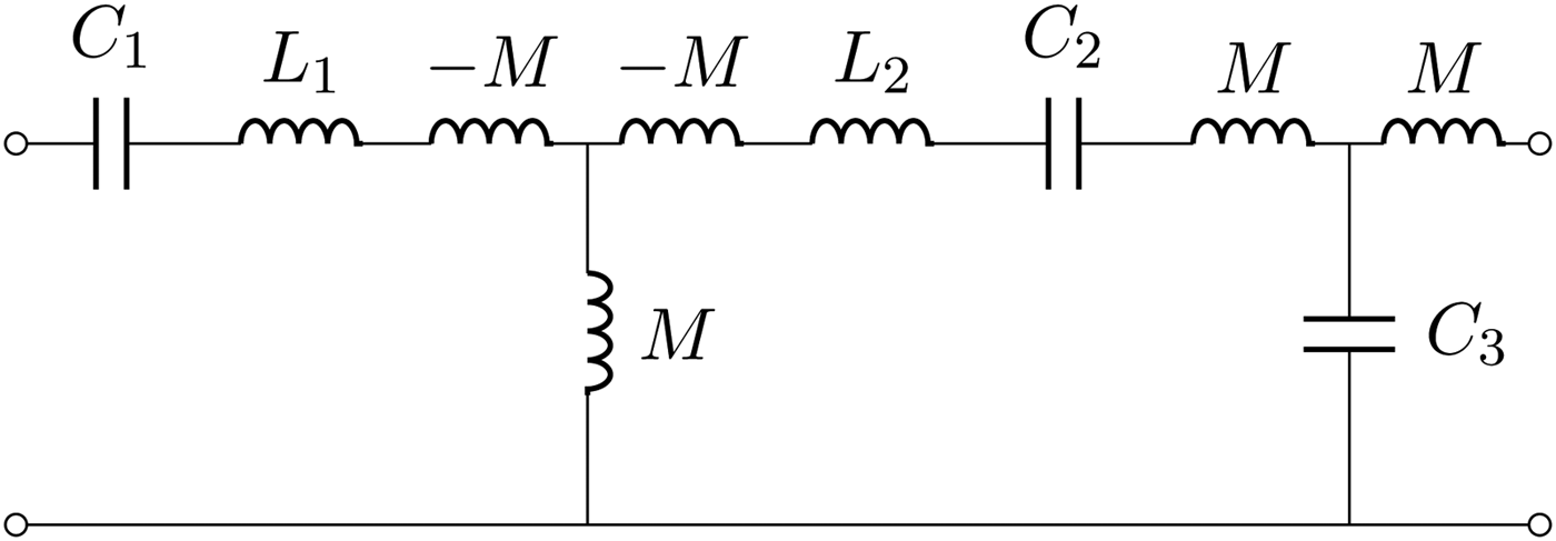
A network that realizes a 1:1 transformer is obtained by considering the series–series network discussed in Section IV-A) and adding at one side one of the immittance inverters shown in Figs 7 and 8. By doing so, we employ one wireless immittance inverter and one lumped immittance inverter as shown in Fig. 12. Note that, in order to recover a 1:1 transformer, the lumped immittance inverter must realize the same value of the wireless one. To this end, by selecting, e.g. the Tee(L, C, L) topology we must use L = M and
 $$C_3 = \displaystyle{1 \over {\omega _0^2 M}}.$$
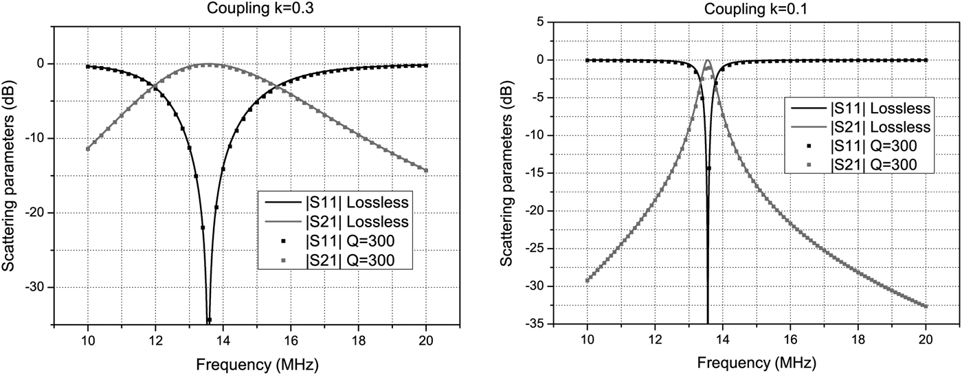
A wideband response for such a network when considering coupling values of k = 0.3, 0.1 is shown in Fig. 13. Note that the capacitances C 1, C 2 are fixed; however, for different values of coupling, i.e. for different M values, the three elements of the lumped immittance inverter should be changed. In this figure, we have also compared the response for the ideal case (no losses) with a realization with a quality factor Q = ω 0L/R = 300. A slight degradation of the response for k = 0.1 is apparent.
A 1:1 transformer realized with one wireless immittance inverter and one lumped inverter. At a selected frequency ω = ω 0, the series of L 1, C 1 and L 2, C 2 realize a short circuit and the entire network behaves as two immittance inverters.
A 1:1 transformer, operating at the frequency of 13.56, has been designed by using an immittance inverter with the Tee(L, C, L) configuration. In the graph are reported the responses in the lossless case and in the case of resonators with Q = 300. The coupling coefficient is also shown in the legend. With reference to Fig. 12, the component values are: L 1 = L 2 = 1 µH, C 1 = C 2 = 137.8 pF. For the figure on the left, we have M = 0.3 µH, C 3 = 459 pF, whereas for the figure on the right we have selected M = 0.1 µH and C 3 = 1.378 nF.
B) Realization with two wireless immittance inverters
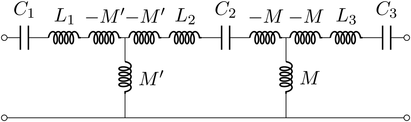
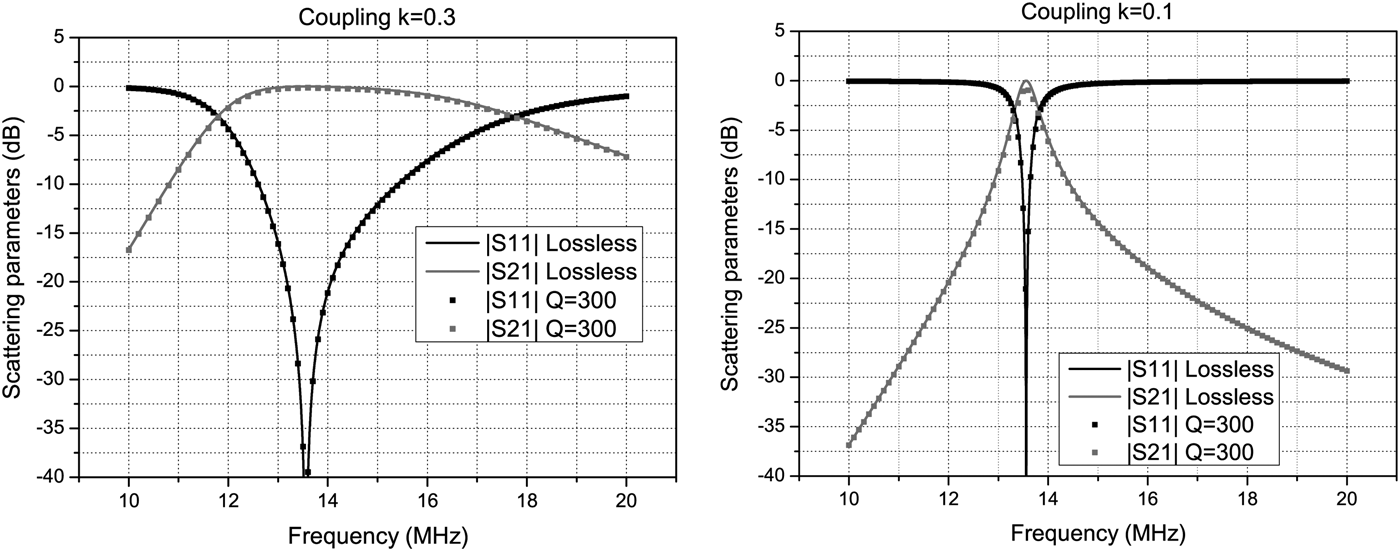
Another useful configuration is the one that uses two wireless immittance inverters as shown in Fig. 14. In this case, an additional resonator with inductance L 3 and capacitance C 3 is added. The elements L 3 and C 3 are physically on the secondary side (e.g. the receiver); while the elements L 1, C 1, L 2, and C 2 are on the primary side. Also on the primary side the two resonators L 1, L 1 and L 2, C 2 are coupled via the mutual inductance M′, which is considered variable. The coupling between L 2 and L 3 (i.e. between primary and secondary side), is denoted by M. By setting M′ equal to M it is apparent that, at the angular frequency of ω 0 we have just two equal immittance inverters in cascade; therefore a 1:1 transformer is realized. The value of this arrangement is that when the coupling M is changed, it is possible to adjust M′ so as to achieve, at least ideally, total power transmission. The results obtainable with this configuration are illustrated in Fig. 15. In the latter figure, we have also compared the response for the ideal case (no losses) with a realization with a quality factor Q = ω 0L/R = 300. Note that we use a pair of coupled inductances (L 2 and L 3) in order to realize the wireless power transfer, while the other coupled inductances (L 1 and L 2) are spatially close together and are used to compensate for different couplings.
A 1:1 transformer realized with two wireless immittance inverters. At a selected frequency ω = ω 0, the series of L 1, C 1, L 2, C 2, and L 3, C 3 realize short circuits and the entire network behaves as two immittance inverters. When M′ is adjusted to be equal to M, a 1:1 wireless transformer is realized.
A 1:1 transformer, operating at the frequency of 13.56 MHZ, has been designed by using two wireless immittance inverters. Note that a pair of coupled inductances are quite separated in space, whereas the other coupled inductances are close together and can be adjusted to compensate for different couplings. In the graph, are reported the responses in the lossless case and in the case of resonators with Q = 300. The coupling coefficient is also shown in the legend. With reference to Fig. 14, the component values are: L 1 = L 2 = L 3 = 1 µH, C 1 = C 2 = C 3 = 137.8 pF. For the figure on the left we have M = 0.3 µH, whereas for the figure on the right we have selected M = 0.1 µH.
VI. CONCLUSION
The problem of MRWPT has been reconsidered from a novel viewpoint. It has been shown that, ideally, the wireless channel should realize a 1:n wireless transformer. By considering the equivalent network of coupled inductances, it is noted that we have a series inductor, an immittance inverter and another series inductor. The series inductors can be compensated by capacitances, so that at the desired frequency, they behave like short circuits. Another immittance inverter, also made by lumped elements, or by coupled inductances, is introduced in order to achieve the behavior of a 1:n transformer.
The proposed approach allows us to design in a systematic manner the wireless channel and avoids problems related to frequency shift and bifurcation of solutions.
Alessandra Costanzo is an Associate Professor of Electromagnetic fields at the University of Bologna, Italy. She has authored more than 140 scientific publications on peer reviewed International Journals and conferences, three chapter books, she holds three international patents. She has developed innovative software platform for the nonlinear/electromagnetic co-simulation of RF systems, excited by modulated sources demonstrating circuit-level analysis of entire MIMO and UWB links, including realistic channel models. She is now involved in wearable energy-autonomous sensors and wireless power transfer systems. She is the MC member of the EU COST action WiPE “Wireless power transfer for sustainable electronics” and she chairs WG1: “far-field wireless power transfer”. She is member of the TPC board member of MTT-S IMS, EUMW, WPTC, and RFID-TA ICUWB. She is the vice chair of IEEE MTT-S TC-26 “Wireless Energy Transfer and Conversion” and member of IEEE MTT-S TC-24 RFID Technologies. She is IEEE senior member.
 Marco Dionigi has received the Laurea degree (110/110 cum laude) in Electronic Engineering from the University of Perugia. He achieved at the same university the title of Ph.D. In 1997, he became an Assistant Professor at the Faculty of Engineering of the University of Perugia. He took part in several research project regarding the development of software tools for waveguide and antenna full wave simulation, the development of permittivity and moisture microwave sensors, the development of a SAR and ultra wideband antennas. He was coauthor of a paper awarded of the “Young Engineers Prize” at the European Microwave Conference 2005 in Paris. He is now involved in the study and development of high efficient wireless electromagnetic power transfer for industrial applications. He is author of more than 70 papers on international journal and conferences.
 Franco Mastri received the Laurea degree (100/100 cum laude) in Electronic Engineering from the University of Bologna, Italy, in 1985. From 1990 to 2004, he was a Research Associate with the Department of Electrical Engineering, University of Bologna, where he has been an Associate Professor of Electrotechnics since 2005. His main research interests include nonlinear-circuit simulation and design techniques (with special emphasis on CAD techniques for large-size problems), nonlinear RF device modeling, nonlinear/RF co-simulation of RF systems, stability, and noise analysis of nonlinear circuits.
 Mauro Mongiardo has received the Laurea degree (110/110 cum laude) in Electronic Engineering from the University of Rome “La Sapienza” in 1983. In 1991 he has become an Associate Professor of Electromagnetic Fields and from 2001 he is the full Professor of Electromagnetic Fields at the University of Perugia. He has been elected Fellow of the IEEE for “for contributions to the modal analysis of complex electromagnetic structures” in 2011. His scientific interests have concerned primarily the numerical modeling of electromagnetic wave propagation both in closed and open structures. His research interests have involved CAD and optimization of microwave components and antennas.
He has served in the Technical Program Committee of the IEEE International Microwave Symposium from 1992; from 1994 he is member of the Editorial Board of the IEEE TRANSACTIONS ON MICROWAVE THEORY AND TECHNIQUES. During the years 2008–2010 he has been the associate editor of the IEEE TRANSACTIONS ON MICROWAVE THEORY AND TECHNIQUES. He is the author or co-author of over 200 papers and articles in the fields of microwave components, microwave CAD and antennas. He is the co-author of the books “Open Electromagnetic Waveguides” (IEE, 1997), and “Electromagnetic Field Computation by Network Methods” (Springer, 2009). Recently, he has co-authored a chapter in the book Wireless Power Transfer – Principles and Engineering Explorations (Intech, 2012), and a chapter in the book Wireless Power Transfer (River publishers, 2012).
 Johannes A. Russer received his Diplom Ingenieur degree in electrical engineering and information technology from the Universität Karlsruhe, Germany, in 2003. In 2004, he joined the University of Illinois at Urbana-Champaign as a research assistant in pursuit of his Ph.D. degree. Since 2007 he has been working for Qualcomm Inc. as an intern. In 2008 Johannes Russer received the second place in the student paper competition of the IEEE MTT-S lnternational Microwave Symposium in Atlanta for the paper “An efficient methodology for the modeling of electromagnetic wave phenomena in domains with moving boundaries”. He has graduated in May 2010 with a Ph.D. thesis on “Methodologies for electromagnetic field modeling for computer aided analysis of multi-domain physical interactions”. Since May 2010 he is working as a Postdoctoral Research Fellow at the Institute for Nanoelectronics of the Technische Universität München. He is working there on the near-field characterization of electromagnetic interference and on methods for numerical modeling of stochastic electromagnetic fields. His research interests concern numerical electromagnetics, network methods in electromagnetic field modeling, multiphysics modeling, and multiscale modeling. He is a member of the IEEE, of the German Informationstechnische Gesellschaft (ITG) and of the Eta Kappa Nu honor society.
 Peter Russer received the Dipl.-Ing. (M.S.E.E.) degree in 1967 and the Dr. techn. (Ph.D.E.E.) degrees in 1967 and 1971, respectively, both from the Vienna University of Technology, Austria. In 1971, he joined the Research Institute of AEG-Telefunkenin Ulm, Germany, where he worked on fiber optic communication, broadband solid-state electronic circuits, statistical noise analysis of microwave circuits, laser modulation and fiber optic gyroscopes. With his research group he realized in 1978 the first optical fiber transmission link for 1 Gbit/s worldwide. From 1981 to 2008, he has been the Professor and head of the Institute for High Frequency Engineering at the Technische Universität München (TUM), Germany. From October 1992 to March 1995, he also has been the Director of the Ferdinand-Braun-Institut für Höchstfrequenztechnik, Berlin. Since 2008 he is Emeritus of Excellence of the TUM and he is now with the Institute for Nanoelectronics of the TUM In 2007 Peter Russer co-founded the Spin-Off company Gauss Instruments GmbH which is now a leading manufacturer of systems for time-domain measurement of electromagnetic interference. He has published five books and more than 900 scientific papers in refereed journals and conference proceedings. He is Life Fellow of the IEEE, member of acatech, the German Academy of Science and Engineering. In 2006 he received the Distinguished Educator Award, and in 2012 the Pioneer Award, both of the IEEE MTT Society and in 2009 he received the Dinstinguished Service Award from the European Microwave Association (EuMA). In 2007 Peter Russer received an honorary Doctor degree from the Moscow University of Aerospace Technologies (MAI). In 2010 Peter Russer has been awarded the Golden Ring of Distinction of the VDE.