I. Introduction
GaN and related compound materials have been intensively studied due to their important practical applications and promising for potential applications [Reference Nakamura, Senoh, Nagahara, Iwasa, Yamada, Matsuahita, Kiyoku and Sugimoto1-Reference Pearton, Zolper, Shul and Ren3]. The existence of high density threading dislocations in GaN films is one of major factors to impede further development of GaN optoelectronic and electronic devices [Reference Ponce and Bour4]. So far the most successful and practical technique for reducing the threading dislocation (TD) density of GaN epilayers is the epitaxial lateral overgrowth (ELO). The TD density of the GaN ELO region could be 4 or more orders lower than the conventionally grown GaN films [Reference Marchand, Wu, Ibbetson, Fini, Kozodoy, Keller, Speck, DenBaars and Mishra5]. Both metalorganic vapor phase epitaxy (MOVPE)[Reference Coltrin, Willan, Bartram, Han, Missert, Crawford and Baca6-Reference Matsushima, Yamaguchi, Hiramatsu and Sawaki9] and hydride vapor phase epitaxy (HVPE)[Reference Zhang, Zhang, Hansen, Boleslawski, Chen, Lu, Shen, Zheng and Kuech10-Reference Kawaguchi, Nambu, Sone, Yamaguchi, Miyake, Hiramatsu, Sawaki, Iyechika and Maeda11] have been used to produce GaN ELO materials with high crystal quality. HVPE is a very useful technique to grow GaN films via both large-area epitaxy and ELO. In HVPE ELO GaN materials, no observable void is found in the coalescence interface and a variety of growth front geometries are observed [Reference Zhang, Zhang, Hansen, Boleslawski, Chen, Lu, Shen, Zheng and Kuech10]. Compared to a non-halide process, a halide process principally offers an advantage of a high lateral-to-vertical growth rate ratio [Reference Carlsson12], which is a key factor influencing the growth front and related dislocation motion in the GaN epilayer grown by ELO. HVPE offers a high growth rate and high material quality for GaN growth [Reference Perkins, Horton, Bandic, McGill and Kuech13,Reference Molnar, Nichols, Maki, Brown and Melngailis14]. The typical growth rate can get 100-200 μm/hr. GaN produced by the HVPE technique does result in a greatly reduced intensity of the defect-based luminescence referred to as the yellow band (YL) when compared to the trimethyl gallium (TMG)-based MOVPE materials. The ability to grow thick GaN film with high quality and obtaining low TD density in ELO GaN films make it possible to get high quality self-standing GaN wafer in a single HVPE growth chamber. In this paper the structural properties of HVPE ELO GaN films, especially coalesced flat-top ELO GaN films, are investigated systematically. The tilting of TDs from the vertical orientation to horizontal or inclined orientations in the GaN “seeding layer” is observed. The lattice tilt due to pileup of tilted TDs is found and the tilt angle is determined. This tilt angle is dependent on ELO growth conditions.
II. Experiments and Results
The GaN ‘substrate’ for ELO growth is an MOVPE grown GaN film on a (0001) sapphire substrate coated with a ∼100nm thick patterned SiO2 layer. The pattern includes an array of 2-4 μm parallel stripe windows openings on a 12 μm period oriented along the 〈1
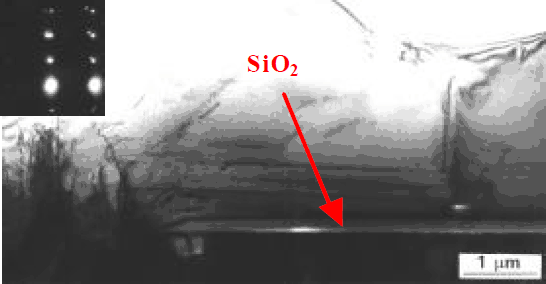
The structural properties of the HVPE ELO GaN films are studied by using transmission electron microscope (TEM), scanning electron microscope (SEM) and high resolution X-ray diffraction (XRD). Atomic force microscope (AFM) is employed to characterize the surface morphology of the ELO GaN films. Fig. 1 shows a cross-sectional SEM picture of a coalesced flat-top HVPE ELO GaN sample. The growth temperature is 1100°C and [NH3]=0.076, [HCl]=0.0023. It could be seen from the figure that the top is flat and the coalescence is perfect. There are no observable voids found at the coalescence interface.
Cross-sectional SEM picture of a coalesced flat-top ELO GaN sample grown by HVPE. There is no void observed at the coalescence interface.

Fig. 2 is an AFM image of the surface morphology in the ELO GaN area of the sample shown in Fig. 1, which clearly shows features characteristics of step-flow growth. There is no detectable step termination in the measured ELO GaN area, indicative of a low TD density [Reference Marchand, Ibbetson, Fini, Kozodoy, Keller, DenBaars, Speck and Mishra15]
A typical AFM image of the surface morphology of the ELO GaN area. No step termination, indicated by surface pits, is observable in the measure area.

Fig. 3 presents a cross-sectional TEM picture of the same sample. The insert is an electron diffraction pattern in the same area. From Fig. 3, most TDs propagated from the MOVPE-grown GaN “seeding layer” along c-axis and bend from the vertical during ELO growth. This change in dislocation motion results in a reduced TD density zone over the masking regions of the ELO GaN film. A lattice tilt results from this change in dislocation direction leading to a new series of diffraction spots in the electron diffraction pattern. The angle between two spot lines is the angle of lattice tilt. In order to precisely determine this tilt angle, high- resolution ω-scan XRD measurements were performed as shown in Fig. 4. In Fig. 4, two separate, approximately symmetric, diffraction peaks appear on two sides of the major diffraction peak. The angle separation of the “tilt” diffraction peak to the major diffraction peak is ∼3.3°. In this case, the full-width-at-half-maximum (FWHM) of the major diffraction peak is 643 arcsec. The asymmetry of two “tilt” diffraction peaks may result from a slight misalignment in the XRD measurement.
A cross-sectional TEM picture of the HVPE ELO GaN film. The change in the direction of the TDs is observable in the picture. The insert is an electron diffraction pattern in the same area. Two sets of diffraction spots indicate that there is a lattice tilt in the ELO area due to pileup of TDs.

High-resolution XRD rocking curve of the HVPE ELO GaN sample shown in Fig. 1. Two separated “tilt” diffraction peaks appear on both side of the major diffraction peak.

Modifications to the ELO growth conditions can alter the TD distribution within the ELO films, as indicated by the intensity of the “tilt” diffraction peaks and their angle spacing from the major diffraction peak. Fig. 5 is a ω-scan XRD rocking curve of a HVPE ELO GaN sample grown using a [NH3]=0.12, [HCl]=0.0022. From Fig. 5, two “tilt” diffraction peaks could be seen again as two wings of the major diffraction peak at an angle of ∼2.4°, as compared to ∼3.3° in the case of lower V/III ratio shown in Fig. 4. The FWHM of the major diffraction peak also decreased to 479 arcsec. The improved structural properties of the crystal coincide, in general, with conditions that lead to improved structural properties in non-patterned growth. This idea has been proved by TEM analysis. The TEM image of the HVPE ELO GaN sample shown in Fig. 5. reveals that many of the TDs initiating in the window area bend into the plane of growth or thread through the ELO region at an oblique angle. The ELO region, particularly in the regions far from the opening windows appear to have a low TD density and should give rise to a reduced XRD linewidth. No observable void is found at the coalescence interface in this case, too.
High-resolution XRD rocking curve of the HVPE ELO GaN sample grown with mole fractions of [NH3]=0.12, [HCl]=0.0022. Again, two separated “tilt” diffraction peaks appear on both side of the major diffraction peak.

III. Discussion
The resulting structure during the ELO process is known to be dependent on the gas phase transport of reactants to the growth front, which is dependent on the growth conditions and mask geometry. The growth chemistry also plays an important role in determining the local growth rates and local V/III ratio. These factors have been shown to have a primary influence on the facet formation in MOVPE growth. The addition of chloride-based species into the growth ambient will decrease the driving force or supersaturation and thus decrease the overall growth rate [Reference Carlsson12]. Reduced supersaturation has often been associated with higher surface transport lengths on the growth front. The specific supersaturation at the growing facet will have this additional factor, i.e. local supersaturation, which affects the local facet determination. The enhanced lateral growth rate of HVPE ELO technique assists in the elimination of the coalescence void at the merge interface [Reference Carlsson12].
The mechanism of the TD bending in the HVPE ELO region is unknown. The influence of a free-bounding surface on the motion of dislocations can play a role. In addition local strains arising from the initial strain state of the GaN “seeding layer” and the thermal expansion difference-based strains due to the presence of the masking materials will affect dislocation motion by developing local strain gradients in the film. The high lateral-to-vertical ratio and high rate of growth in HVPE, when compared to MBE or MOVPE, aid in the development of a merged front free of a coalescence void. Increased V/III ratio lead to improved materials properties, while maintaining a void-free coalescence, in ELO as in the non-masked growth.
IV. Conclusions
The dependence of the structural properties of HVPE ELO GaN films on gas phase V/III ratio has been investigated in this paper. A lower V/III ratio was found to lead to improved ELO materials, as determined by XRD measurement. No observable voids were present at the coalescence interface. A lattice tilt is seen in all of the HVPE samples characterizing the deflection of the <0001> planes between the GaN grown over the masking region and the initial window opening.
Acknowledgements
R. Zhang, Y, Shi, Y.G. Zhou, B. Shen, Y.D. Zheng thank the financial support of the China “863” national high-tech development program and National Natural Science Foundation of China with contracts #69976014, #69636010, #69806006, #69987001. The authors would like to acknowledge the financial support of the ONR MURI on Compliant Substrates, and the facilities support of the NSF Materials Research Science and Engineering Center on Nanostructured Materials and Interfaces, USA.