
1.1 Graphene Band Structure
Graphene is a two-dimensional structure of carbon atoms. Single-layer graphene consists of only one layer of carbon atoms. A carbon atom has six electrons occupying the 1s2, 2s2, 2px, and 2py atomic orbitals. When carbon atoms are brought together, one electron from the 2s orbital is promoted to the 2pz orbital for the formation of hybrid orbitals. In diamonds, the 2s, 2px, 2py, and 2pz orbitals are mixed to form four sp3 hybrid orbitals for each carbon atom; therefore, each carbon atom is joined with four neighbors by overlapping their sp3 hybrid orbitals. In graphite, instead of four sp3 hybrid orbitals, three sp2 hybrid orbitals are formed through mixing of the 2s, 2px, and 2py orbitals, while the fourth orbital remains as 2pz. Overlapping sp2 hybrid orbitals from two adjacent atoms creates a strong σ covalent bond (C‒C bond); these in-plane σ bonds connect each carbon atom to three neighbors. The remaining 2pz orbitals of these carbon atoms form π bonds, which are responsible for binding carbon layers together in graphite. Because π bonds are much weaker than σ bonds, graphite has a low shear strength so that its carbon layers can be easily detached. For monolayer graphene, these nearly free π electrons are responsible for most of its experimentally observed electronic and optical properties. Because the Pauli exclusion principle requires that π electrons from different carbon atoms do not occupy the same state, the large number of closely packed carbon atoms in graphene causes degenerate energy levels to split into continuously distributed nondegenerate levels of allowed energy states, forming energy bands.
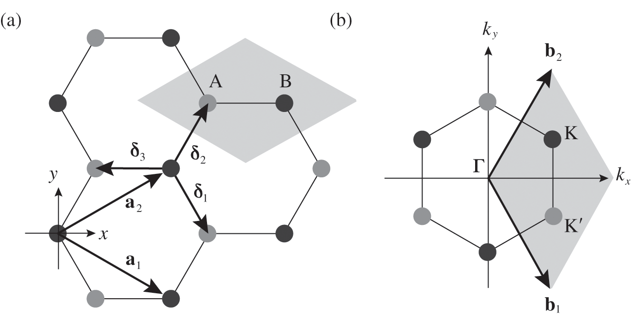
The real-space two-dimensional honeycomb lattice of graphene is shown in Figure 1.1(a). The distance between two neighboring carbon atoms in graphene is
 (1.1)
(1.1)
The primitive lattice vectors are
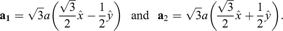 (1.2)
(1.2)
Therefore, the lattice constant is
 (1.3)
(1.3)
The area Ap of a primitive unit cell can be obtained as
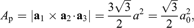 (1.4)
(1.4)
where  is the unit vector that points in the direction perpendicular to the plane of the two-dimensional graphene lattice. We also find that the vectors connecting adjacent carbon atoms are
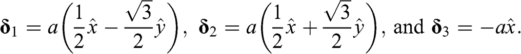 (1.5)
(1.5)
as shown in Figure 1.1(a).

Figure 1.1 (a) Real-space honeycomb graphene lattice. The lattice consists of two overlapping Bravais sublattices, A (gray dots) and B (black dots). The primitive unit cell is drawn as a shaded area.  and
and  are the primitive lattice vectors.
  ,
,  , and
, and  are vectors pointing from a B atom to its nearest A atoms. (b) Brillouin zone of graphene drawn as a shaded area.
  and
and  are the primitive vectors of the reciprocal lattice. Dirac points
  (black dots) and
  (gray dots) are marked.
The corresponding Brillouin zone of the lattice in Figure 1.1(a) is shown in Figure 1.1(b). The primitive vectors of the reciprocal lattice are
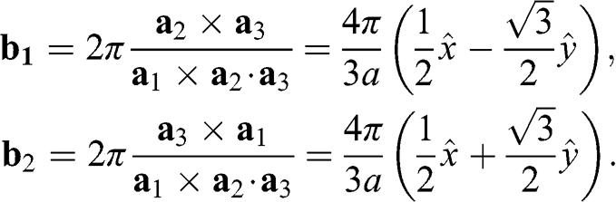 (1.6)
(1.6)
We can also find the vector  that is perpendicular to the plane of the two-dimensional reciprocal lattice. Therefore,
 (1.7)
(1.7)
where  is the Kronecker delta function:
  if
if  , and
, and  if
if  .
.
The honeycomb lattice of graphene is not a Bravais lattice because the locations of all carbon atoms cannot be generated by the translation
 (1.8)
(1.8)
where m and n are integers. The lattice structure of graphene consists of two overlapping Bravais sublattices A and B, and thus a primitive unit cell contains two carbon atoms, as shown in Figure 1.1(a). All of the carbon atoms on the same sublattice, but not those on the two different sublattices, are connected by the vector  .
.
The electronic band structure of graphene can be obtained by using the tight-binding model. We start from a tight-binding Hamiltonian  for the Schrödinger equation:
 (1.9)
(1.9)
The wave function  is given by the linear superposition of orbital functions
  :
:
 (1.10)
where N is the number of unit cells,  is the ground state of the
  electron of an isolated carbon atom that is located at
  , and the index l runs over all carbon atom points on the graphene lattice. Equation (1.10) is of the Bloch form because
  , where
  or 2. From the symmetry point of view, all atoms on sublattice A are geometrically identical; in other words, the surrounding is the same when viewing the graphene lattice from any atom on sublattice A. The same can be said for all atoms on sublattice B. No difference can be seen when viewing the graphene lattice from different atoms on the same sublattice. However, the atoms on sublattice A are not geometrically identical to those on sublattice B. By comparing the scenery in a certain direction, it is possible to tell the difference between viewing the graphene lattice from one atom on sublattice A and viewing it from one on sublattice B. Therefore, the wave function in (1.10) has only two independent coefficients for
  :
:  and
and  , which respectively represent the amplitudes of the wave functions at carbon sites on sublattices A and B. Thus, (1.10) can be rewritten as a linear superposition of two Bloch functions
  and
and  that are respectively wave functions for sublattices A and B:
 (1.11)
where  and
and  run over all of the carbon atoms on sublattices A and B, respectively. The wave functions
  and
and  are normalized, and the overlap of
  and
and  is negligible [Reference Reich, Maultzsch, Thomsen and Ordejón1], so that
  . Therefore,
  and
and  form the basis for the graphene wave functions.
By multiplying both sides of (1.9) by  , we obtain
 (1.12)
In (1.12), all of the interactions among A atoms and those between A atoms and B atoms are considered. However, it is very difficult to solve for the eigenenergy from (1.12) where all interactions are accounted for. To avoid such difficulty, (1.12) is simplified by taking the approximation of considering only the self-interaction of each carbon atom at a lattice point and the interactions of the atom with its three nearest neighbors; all long-range interactions are assumed to be much weaker than these interactions and are thus ignored. Within this approximation, (1.12) takes the simple form:
 (1.13)
By multiplying both sides of (1.11) by  and taking the same approximation, we have
 (1.14)
Equations (1.13) and (1.14) can be expressed in a matrix form for the eigenenergy equation of the system:
 (1.15)
where
 (1.16)
is the self-interaction energy, and
 (1.17)
is the nearest-neighbor hopping energy in graphene. The nearest-neighbor hopping energy  is experimentally measured to have a value of
  [Reference Peres2–Reference Abergel, Apalkov, Berashevich, Ziegler and Chakraborty4], which is the same as that found for graphite.
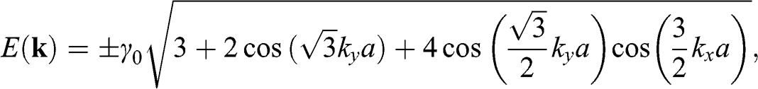
The nontrivial eigenvalues of (1.15) yield two eigenenergies:
 (1.18)
where the plus sign is for the conduction band, which has higher energy, and the minus sign is for the valence band, which has lower energy. The conduction band and the valence band described by (1.18) are also called the  band and the
  band, respectively. Equation (1.18) can be written in another form that is frequently seen in the literature [Reference Wallace5,Reference Castro Neto, Guinea, Peres, Novoselov and Geim6]:
 (1.19)
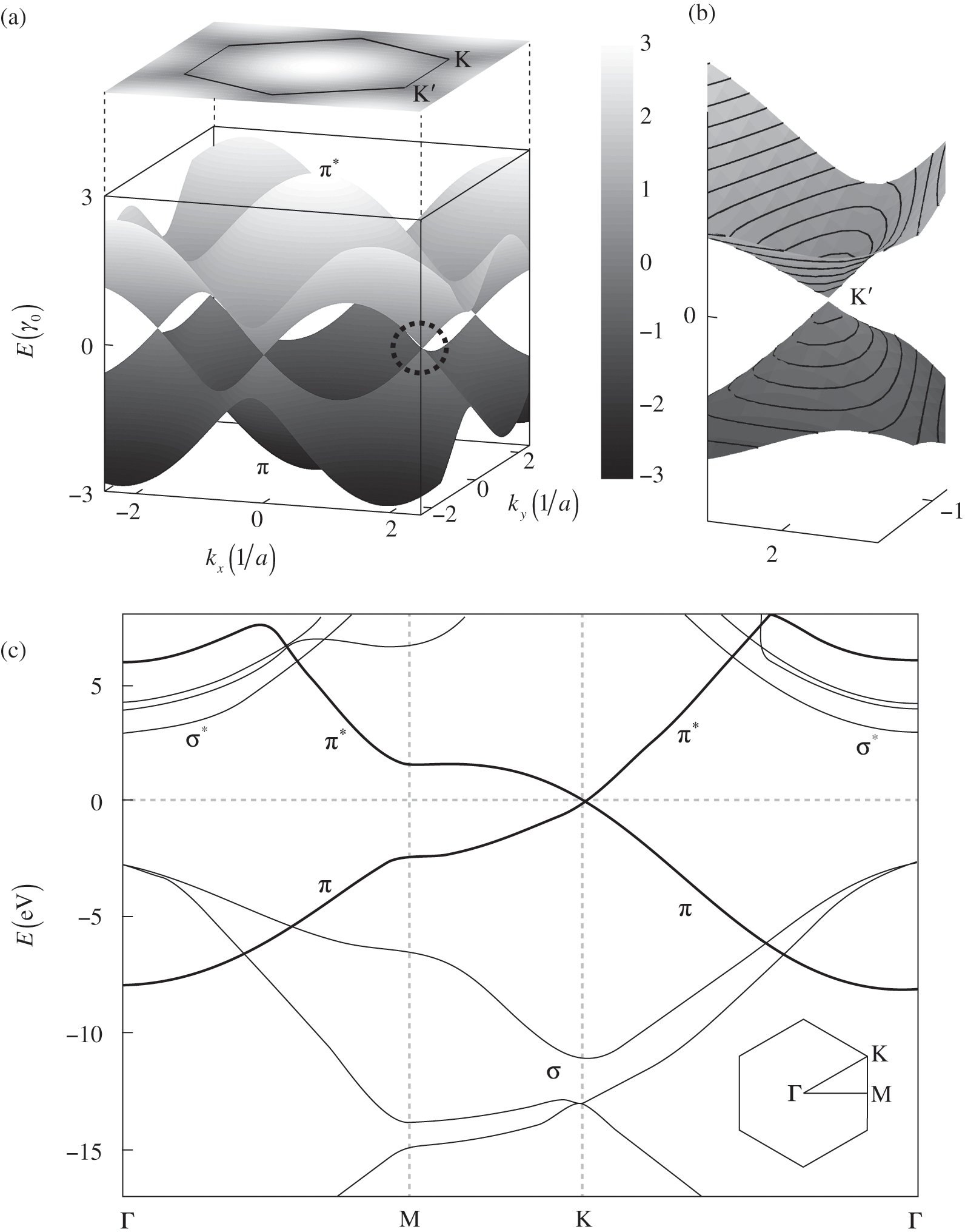
The energy band structure described by (1.19) is plotted in Figure 1.2(a). At the Г point ( ), we find the eigenenergies
  from (1.19), which are associated with the eigenstates
  , respectively. The eigenenergy
  for the valence band is associated with symmetric bonding orbitals such that the amplitudes
  and
and  of the wave functions for sublattices A and B have the same sign. By contrast, the eigenenergy
  for the conduction band is associated with antibonding orbitals such that the amplitudes
  and
and  of the wave functions for sublattices A and B have opposite signs. An eigenstate of graphene is not necessarily bonding or antibonding, however; most eigenstates are a mixture of both bonding and antibonding orbitals. As we shall see in the following, only along a specific set of directions can the eigenstates be described by purely bonding or antibonding orbitals. The conduction band (
 band) and the valence band (
 band) are symmetric with respect to the
  plane, as shown in Figure 1.2(a). Note that the long-range interactions of carbon atoms beyond the nearest neighbors are ignored in the above analysis. When these long-range interactions are accounted for, we find that the
  and
and  bands are actually not symmetric to each other, as seen in Figure 1.2(c), where we also show the
  and
and  bands contributed by the
  bonds.

Figure 1.2 (a) Band structure of graphene plotted using (1.19) while setting the self-interaction energy to be  . The top surface of a higher energy is the conduction band (
 band), and the bottom surface of a lower energy is the valence band (
 band). The conduction band is projected onto a two-dimensional plane on the top. The circled region near the Dirac point
  is enlarged in (b). (c) Full band structure of graphene. The thick curves are the
  and
and  bands, and the thin curves are the
  and
and  bands [Reference Sedelnikova, Bulusheva and Okotrub7].
As can be seen in Figure 1.2(a), the conduction band touches the valence band at  . The self-interaction energy
  can be taken as the reference level by setting it to be 0 for simplicity so that an electron in a state on the conduction band has a positive energy and that in a state on the valence band has a negative energy. Then, (1.19) can be simplified as
 (1.20)
where the plus sign represents the conduction band and the minus sign represents the valence band. The points at 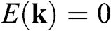 are called the Dirac points; the vicinities of these points are referred to as the valleys, where the graphene band structure can be described by the relativistic Dirac equation, which is further discussed in the following section. Corresponding to the two distinct sublattices A and B in the real space, there are two distinct groups of Dirac points
  and
and  in the k space. Inside the Brillouin zone drawn in Figure 1.1(b), two Dirac points can be found at the k-space locations represented by the reciprocal space vectors:
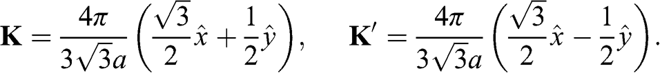 (1.21)
Another popular choice of the k-space locations of  and
and  in the literature is to select the
  and
and  points on the ky axis so that they are mirror symmetric with respect to the kx axis; the physics and the results obtained in the following are unchanged by this alternative selection. It can be easily shown using (1.20) that
  at these Dirac points.
For perfectly intrinsic graphene, the chemical potential, i.e., the Fermi level, is located at the energy level of the Dirac points,  , so that the valence band is completely filled and the conduction band is completely empty. As most physics and carrier transitions happen at energy levels around the chemical potential, we shall rewrite (1.20) by shifting the origin of the k space to one of the Dirac points and assume a small k to simplify (1.20). Substituting
  in (1.20) with
  or
or  , we obtain, for
  in the vicinity of a Dirac point,
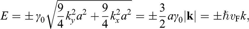 (1.22)
where  is the reduced Planck’s constant and
 (1.23)
is the Fermi velocity in graphene, the physical meaning of which will become clear in Section 1.5. Equation (1.22) indicates that there is a region in the k space around each Dirac point where the carrier energy is linearly proportional to the wave number measured with respect to the given Dirac point. This region is called the Dirac cone, as shown in the insert in Figure 1.2(b). Because (1.22) can also be derived from the massless Dirac equation, electrons on the Dirac cone are also called Dirac electrons.
The Hamiltonian around the  point is obtained in the same way as (1.22) is obtained. By substituting
  with
with  in (1.15) to set the origin of the k space at the
  point, the off-diagonal matrix elements for
  become
 (1.24)
and
 (1.25)
The coefficients of  and
and  can be simplified by rotating both the
  and
and  coordinate axes counterclockwise by 30 degrees through the unitary transformation
 (1.26)
Using (1.26), we obtain the relation  from (1.24) and (1.25). By dropping the prime symbols,
  and
and  , to simplify the notation, the Hamiltonian near the
  point for
  can be expressed as
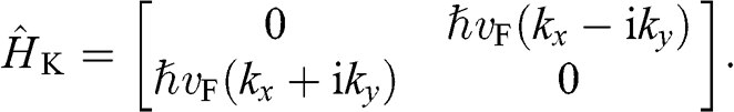 (1.27)
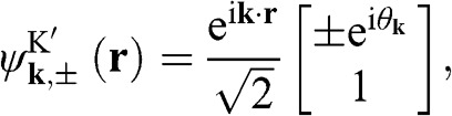
The corresponding eigenfunctions are
 (1.28)
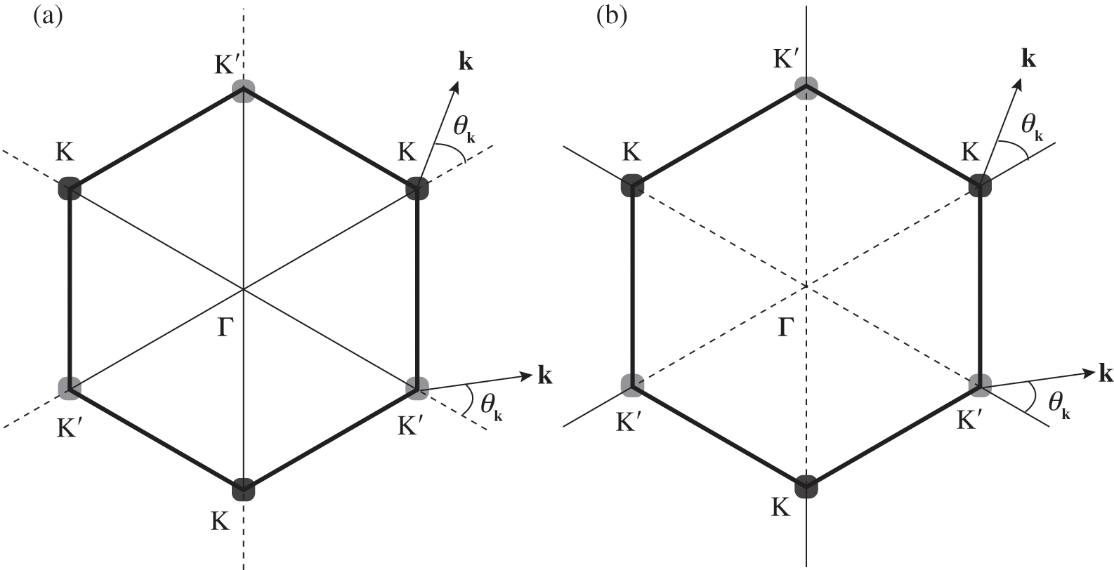
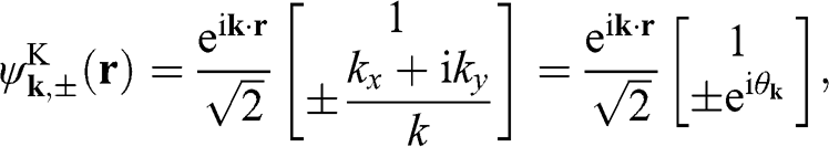
where the  signs correspond to the signs of the eigenenergies given in (1.22), and
  is the polar angle measured between
  and the rotated
  axis as shown in Figure 1.3(a) for the
  point.
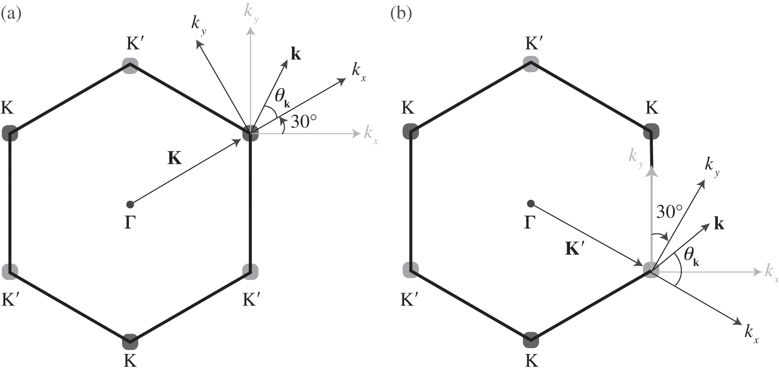
Figure 1.3 Wave vector  near (a) the
  point, and (b) the
  point. The Hamiltonian near the
  or
or  point is obtained by rotating the coordinate from the gray axes to the black axes. The angle
  is measured with respect to the rotated
  axis.
axis.
Similarly, the Hamiltonian near the  point is obtained by substituting
  with
with  in (1.15) and taking the unitary transformation by rotating the axes 30 degrees clockwise; the result for
  is
is
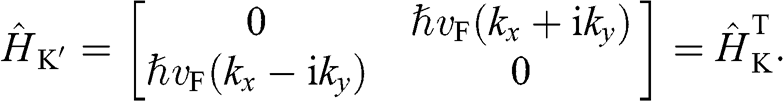 (1.29)
The eigenfunctions are
 (1.30)
where the  signs correspond to the signs of the eigenenergies given in (1.22), and
  is the polar angle measured between
  and the rotated
  axis at the
  point, as shown in Figure 1.3(b). From (1.28) and (1.30), it is clear that for the conduction band, the eigenstate is antibonding at
  and bonding at
  , as shown in Figure 1.4(a). By contrast, the eigenstate is bonding at
  and antibonding at
  for the valence band, as shown in Figure 1.4(b).
Equations (1.27) and (1.29) are often written as
 (1.31)
for an electron near a  point and as
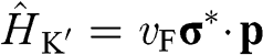 (1.32)
for an electron near a  point, where
  and
and  is the Pauli vector:
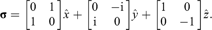 (1.33)
Note that 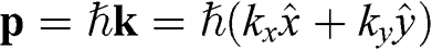 with
with  for the
  electrons in monolayer graphene because they only move through the graphene lattice on the xy plane of a monolayer graphene sheet.

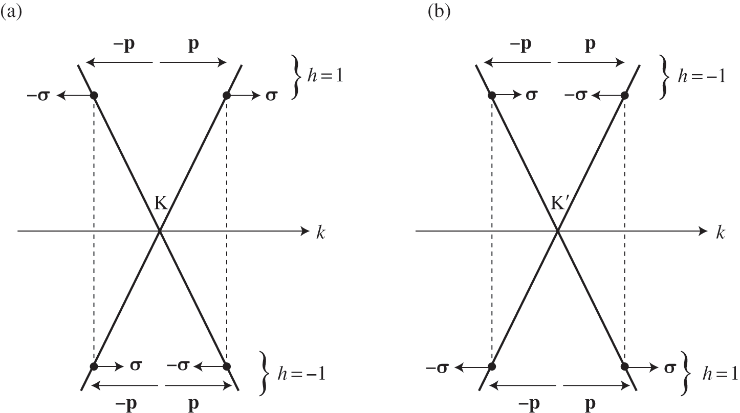
Figure 1.4 Antibonding (solid thin lines) and bonding (dotted lines) states in (a) the conduction band and (b) the valence band.
In fact, the Hamiltonian of graphene near a  or
or  point has the form identical to that of a spin one-half particle in a magnetic field; its eigenfunctions are two-component spinors, as seen in (1.28) and (1.30). In the case of graphene,
  does not really represent an electronic spin, but a pseudospin that indicates the sublattice on which the electron is located. We can define a helicity operator
  to find the projection of the momentum along the pseudospin direction; then it can be shown that
  . The positive sign gives positive helicity, meaning that the momentum of an electron on the conduction band is parallel to the pseudospin, whereas the negative sign gives negative helicity, meaning that the momentum of an electron on the valence band is antiparallel to the pseudospin. The relation among the helicity, the carrier momentum, and the pseudospin are shown in Figure 1.5. Because of the conservation of pseudospin, a right-moving electron on the conduction band cannot be scattered into a left-moving electron on the conduction band or into a right-moving electron on the valence band. Such scattering requires the pseudospin to be flipped from
  to
to  for an electron near the K point, or flipped from
  to
to  for an electron near the
  point, neither of which is allowed. Similarly, scattering of a left-moving electron on the conduction band into a right-moving electron on the conduction band or into a left-moving electron on the valence band is also forbidden. Nevertheless, such scattering events can happen when there exists a short-range potential that acts differently on sublattices A and B, thus breaking the symmetry between the two sublattices.

Figure 1.5 Helicity h, pseudospin  , and momentum
  of an electron near (a) the
  point, and (b) the
  point. The directions of
  and
and  are shown. In the case of a hole, the direction of momentum is reversed. Due to the conservation of pseudospin, an electron or a hole cannot be scattered into an electron or a hole of a different pseudospin.
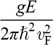
1.2 Density of States and Carrier Concentration
With the band structure near the Dirac point described by (1.22), the density of electron states of graphene in the energy range between  and
and  for
for 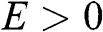 near the conduction band edge is
 (1.34)
and that for  near the valence band edge is
 (1.35)
where  is the area of the graphene sheet and
  is the total degeneracy due to the spin degeneracy and the valley degeneracy (two valleys
  and
and  in one Brillouin zone). Because of the symmetry between the conduction band and the valence band with respect to the Dirac point,
  for the same absolute value
  of energy.
From (1.34) and (1.35), the surface concentrations of electrons and holes of a graphene sheet are, respectively,
 (1.36)
where
 (1.37)
is the equilibrium Fermi–Dirac distribution function for a chemical potential  at a temperature T, and
  is the Boltzmann constant. The probability of finding an electron in a state at the energy level E is
  , and the probability of finding a hole in a state at the energy level E is
  . When the condition
  is satisfied,
  is approximately a Heaviside step function
  , which has a value of 1 for
  and 0 for
  . Therefore, for
  ,
,
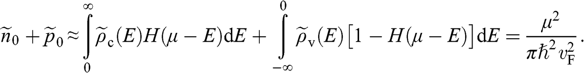 (1.38)
In this book, we use a tilde for a 2D quantity to clearly distinguish it from its 3D counterpart in order to avoid confusion. Therefore, the surface electron density  , the surface hole density
  , and the densities of states
 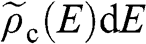 and
and  of graphene are all numbers per unit area in the unit of
  , or
, or  ; whereas their 3D counterparts,
  ,
,  ,
,  , and
, and  , are all numbers per unit volume in the unit of
  , or
, or  .
.
1.3 Fermi Energy, Chemical Potential, and Fermi Level
Here we clarify the terminologies and notations that are sometimes swapped or not clear in some books and literature: the Fermi energy  , the chemical potential
  , and the Fermi level. The Fermi energy
  is defined as the energy difference between the highest energy level and the lowest energy level that are occupied by electrons at the absolute zero temperature,
  . Therefore, the Fermi energy is defined only at
  ; it is theoretically defined but experimentally cannot be exactly measured because the absolute temperature can never truly reach zero. For a metal, the Fermi energy is usually taken to be the kinetic energy of the electron that occupies the highest energy level at
  ; therefore, it is always positive. For graphene, we take the Fermi energy to be the total energy of the electron that occupies the highest energy level at
  , which can be either positive or negative, or zero, if the reference point of zero energy is defined at the Dirac point, as seen below. By contrast, the chemical potential is meaningful at any temperature because it is a statistical reference for the total energy, including the potential energy and the kinetic energy, of a particle in a system in thermal equilibrium. In solid-state physics, the chemical potential
  usually refers to the change of free energy when an additional electron is added to a system. The effect of
  is best observed in the Fermi–Dirac distribution
  , where one can see that at zero temperature, the minimum energy required to add an additional electron is
  because below it electronic states are all occupied. In the electronic devices context, the term Fermi level usually refers to the chemical potential
  . However, in semiconductor physics, the Fermi level is usually denoted by the symbol
  though it refers to the chemical potential
  . To avoid confusion with the Fermi energy, in this book we use the symbol
  to represent only the Fermi energy while using the symbol
  to represent the chemical potential and the Fermi level.
From the above discussions, we see that  is a function of temperature:
  . In the case when
  lies within the conduction band,
  is positive and can be found from the definition
  at zero temperature. In the case when
  lies within the valence band, we define
  to be negative using the definition
  at zero temperature. The temperature dependence of
  of graphene can be found by recognizing the fact that each additional thermally excited electron always comes with the creation of a hole to result in an electron–hole pair. Therefore, for a given piece of graphene, the difference between the electron concentration and the hole concentration,
  , is a conserved quantity that is independent of temperature. In the case when
  at zero temperature so that the chemical potential lies within the conduction band, we have
  and
and  from (1.38). Therefore we can relate
  and
and  by combining (1.36) and (1.38) to write
 (1.39)
which can be written in a compact form:
 (1.40)
from which  can be numerically obtained. In the case when
  lies within the valence band so that
  , we have
  and
and  from (1.38). Then, following a procedure similar to the above, we obtain
 (1.41)
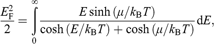
When  , the integrals for both (1.40) and (1.41) approach
  , and we have
 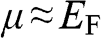 .
.
1.4 Temperature Dependence of Carrier Concentration
The dependence of the free carrier concentration  of graphene on temperature is shown in Figure 1.6 for
  . The characteristics obtained under two different approximations are compared to the exact temperature dependence of the carrier concentration obtained without approximations. The dotted line is the low-temperature approximation given by (1.38), and the dashed curve is obtained from (1.36) by assuming
  independent of temperature. The solid curve is the exact result calculated from (1.36), with
  varying with temperature obtained from (1.40). As can be seen, the dotted line is accurate only when the temperature is low, and the dashed curve overestimates the carrier concentration. In general, a higher temperature leads to a higher carrier concentration because of thermally excited electron–hole pairs.
Figure 1.6 Carrier concentration for  as a function of temperature calculated under different assumptions. The dotted line and the dashed curve are obtained under the low-temperature approximation and the constant
  approximation, respectively, while the solid curve is the exact result.
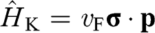
1.5 Carrier Velocity and Effective Mass
In the preceding sections, we regard a charge carrier in graphene as a wave that has a momentum of  and an energy of
  . In this section, we treat the wave packet as a particle that has a velocity equal to the group velocity of its wave packet. For an isotropic two-dimensional material such as graphene, the phase velocity
  and the group velocity
  of an electron that has a momentum of
  and an energy of
  are, respectively,
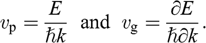 (1.42)
For an electron in graphene near a Dirac point, the carrier energy is linearly proportional to the momentum:  ; thus, we find that
 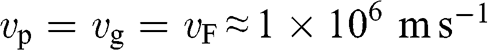 , independent of the electron energy. The same conclusion applies to a hole in graphene near a Dirac point. Therefore, the parameter
  represents both the group velocity and the phase velocity of a carrier in graphene. The parameter
  also represents the Fermi velocity because a carrier that has a kinetic energy equal to the Fermi energy also moves at a group velocity of
  in the vicinity of a Dirac point. This result is distinctively different from the energy-dependent group velocity
 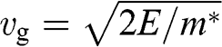 of a carrier in an ordinary material, where
  is the effective mass of an electron in the conduction band of the material or that of a hole in the valence band.
The linear energy–momentum relation of the carriers in graphene resembles the relativistic Dirac equation. Unlike the Schrödinger equation, the Dirac equation accounts for special relativity through the relativistic energy–momentum relation:
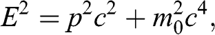 (1.43)
where 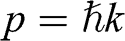 is the particle momentum,
  is the rest mass of the particle, and c is the speed of light. If we compare the energy–momentum relation given in (1.22) for a carrier in graphene with the relativistic energy–momentum relation given in (1.43), we find that a carrier in graphene has an effective speed of
 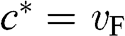 and a zero effective rest mass of
  . Therefore, the carriers in graphene are often called massless Dirac fermions.
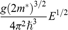
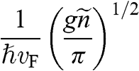
In contrast to the effective rest mass, an effective mass associated with the acceleration of a carrier in graphene under the influence of an external force can be defined. For example, when a carrier in graphene is accelerated by an external magnetic field, the carrier follows a circular orbit dictated by Maxwell’s equations. If the area enclosed by the orbit is  , the cyclotron effective mass is defined as [Reference Castro Neto, Guinea, Peres, Novoselov and Geim6,Reference Miller, Kubista and Rutter8,Reference Novoselov, Geim and Morozov9]
 (1.44)
With  and
and  , we obtain
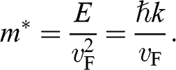 (1.45)
Therefore, the cyclotron effective mass is energy dependent, and (1.45) manifests the mass–energy equivalence from special relativity, namely,  with
with  .
.
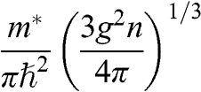
In solid-state physics, the effective mass of a charge carrier is often calculated as  because the energy of a carrier is quadratically dependent on its momentum near a conduction band minimum or a valence band maximum of an ordinary three-dimensional solid-state material. However, in the case of graphene, this relation is invalid because it gives a mathematically divergent result due to the fact that
  for a carrier in graphene. The reason is that the energy of a carrier in graphene near a Dirac point varies with its momentum not quadratically but linearly:
  from (1.22). Thus the assumption of a constant effective mass given by
  is not valid for a carrier in graphene. Instead,
  for a carrier in graphene can be calculated using the momentum relation
  so that
 (1.46)
which gives a result that is consistent with (1.45). This relation yields  at the Dirac point where
  ; this result is also conceptually consistent with the zero effective rest mass for a carrier in graphene discussed above.
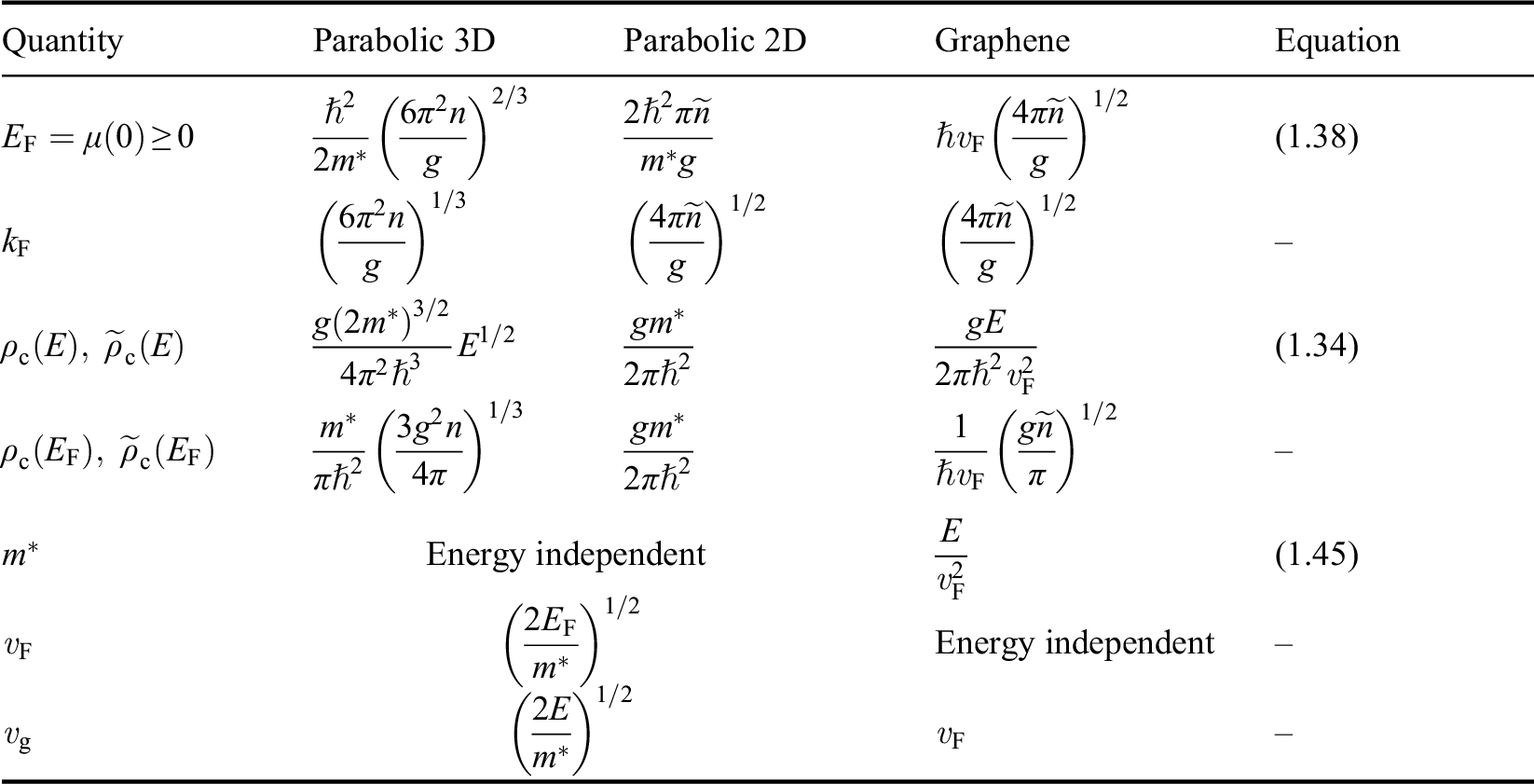
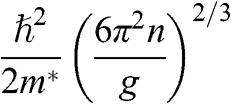
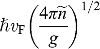
The comparison of parabolic 2D/3D systems and monolayer graphene for various physical quantities is presented in Table 1.1.
| Quantity | Parabolic 3D | Parabolic 2D | Graphene | Equation |
|---|---|---|---|---|
| 
| 
| 
| (1.38) |

| 
| 
| 
| – |
| 
| 
| 
| (1.34) |
| 
| 
| 
| – |

| Energy independent | 
| (1.45) | |

| 
| Energy independent | – | |

| 
| 
| – | |
a: In this table, the parameters of an electron in a conduction band are listed; those of a hole in a valence band can be similarly expressed.  is the energy of the electron measured with respect to the conduction band edge, by setting
  for the conduction band minimum of a parabolic system and
  for graphene.
  is the electron density of a 3D system and
  is the electron density of a 2D system including graphene, in the limit that
  .
.  is the total degeneracy including spin degeneracy.
1.6 Band Structure of Multilayer Graphene
When multiple layers of graphene are brought together to form a sheet of multilayer graphene, the interlayer interaction can fundamentally change the band structure. In this section, the band structures of AA and AB (Bernal) stacking orders are derived. Other possible stacking arrangements are discussed at the end.
1.6.1 AB Stacking Order
In AB-stacked multilayer graphene, the arrangement of layers follows the αβαβ … order. Figure 1.7 illustrates the AB stacking by showing one set of α and β layers. Nearest-neighbor intralayer and interlayer interactions are considered, as shown in Figure 1.7(a); high-order interactions beyond nearest neighbors are neglected for simplicity. The intralayer interaction energy is  , defined in (1.17), whereas the interlayer interaction energy is characterized by a different off-diagonal parameter
  in the Hamiltonian. The top layer (β layer) is shifted relative to the bottom layer (α layer) by one C–C distance, as shown in Figure 1.7(b).

Figure 1.7 (a) Intralayer ( ) and interlayer (
 ) interactions of AB-stacked multilayer graphene showing one set of α and β layers. (b) Top view of (a), showing the overlap between α (bottom) and β (top) layers. (c) Side view of (a). A chain of alternating A and B carbon atoms connected through interlayer interactions of energy
  along the z direction is shown.
The band structure of N-layer AB-stacked multilayer graphene can be obtained in a manner similar to the derivation of the band structure of monolayer graphene. As shown in (1.27), after proper transformation the Hamiltonian at the  point for intralayer interactions can be expressed in terms of the energy parameters
  with
with  . Therefore, the tight-binding Hamiltonian at the
  point for AB-stacked multilayer graphene can be expressed in a form similar to (1.27) as [Reference Min and MacDonald10]
 (1.47)
In (1.47), the basis is taken to be  , with the eigenvector
  , where
  and
and  correspond to the sublattice A or B of layer n. By applying the eigenvalue equation
  , we find from (1.47) the following coupled difference equations,
 (1.48)
 (1.49)
where  and
and  .
.
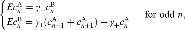
We first check if  is a nontrivial solution for the coupled equations of (1.48) and (1.49). For
  , we have
  for odd n and
  for even n. If we assume nonzero
  and
and  , we obtain from (1.48) and (1.49) a trivial solution with all c coefficients being zero. However, if we assume
  , we have rows in (1.47) that are identically zero; thus,
  for even n and
  for odd n are decoupled and can assume any value. Other coefficients can be either zero or nonzero, determined by (1.48) and (1.49) and the number of layers. Therefore,
 (1.50)
represents a nontrivial solution for the coupled equations of (1.48) and (1.49).
For  , we can simplify (1.48) and (1.49) as
 (1.51)
 (1.52)
Then, by defining  for odd n and
  for even n, the coupled equations of (1.51) and (1.52) can be expressed in a single simplified form:
 (1.53)
where  . Thus we have transformed the original problem expressed in the coupled equations of (1.48) and (1.49) into a chain of N atoms with eigenenergy
  while considering only the nearest-neighbor interactions characterized by the interlayer interaction energy
  , as shown in Figure 1.7(c). With the constraint that
  , we find the solutions of (1.53) as
 (1.54)
where  . Therefore, we find N eigenvectors for N-layer graphene. By plugging (1.54) back into (1.53), we find the eigenenergies:
 (1.55)
To gain more physical insight for (1.55), we can regard N-layer graphene as a Fabry–Pérot cavity in which an electromagnetic wave is confined in the direction perpendicular to the multilayer graphene surface, which is taken to be the z direction [Reference Mak, Sfeir, Misewich and Heinz11]. The boundary condition  implies that the wave function vanishes at
  and
and  beyond the first and
  layers. The distance between the locations of
  and
and  layers is
  ; therefore, the effective length of the Fabry–Pérot cavity is
 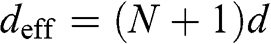 , where
 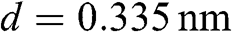 is the distance between two neighboring graphene layers in AB stacking. A standing wave can form within the multilayer graphene structure with two opposite wave vectors of equal magnitude in the z direction:
 (1.56)
Therefore, as the thickness of the multilayer graphene increases with the number N of layers, the number of the allowed values of quantized  also increases. By using (1.56), we can rewrite (1.55) as
 (1.57)
which gives the eigenenergy of N interacting carbon atoms with  being the wave number along the direction normal to the graphene surface. Indeed, if the in-plane wave numbers have zero values so that
  and
and  , the original problem represented by (1.48) is tantamount to the chain of carbon atoms along the z direction shown in Figure 1.7(c). The eigenenergy is simply
  because
  in the relation
  .
.
When  and
and  are not both zero so that
  and
and  , the eigenenergy E can be found from the relation
  , which gives
 (1.58)
where  is the in-plane wave number, in contrast to the out-of-plane wave number
  . In the limit that
  , (1.58) has two small-
 solutions:
 (1.59)
and
 (1.60)
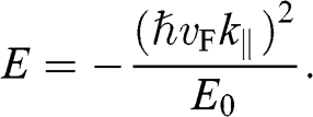
Note that in both (1.59) and (1.60),  varies quadratically, not linearly, with
  . By defining the effective mass for these quadratic bands as
 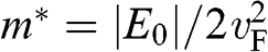 , the first solution (1.59) has the form of
 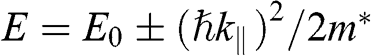 , and the second solution (1.60) has the form of
 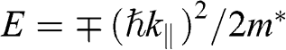 , where the upper signs are taken when
  and the lower signs are taken when
  . Accordingly, the energy bands given by (1.59) and (1.60) are called massive bands, in contrast to the massless Dirac bands of monolayer graphene.
For even N, there are N different values of  given by (1.55). Therefore, (1.59) and (1.60) respectively give N energy bands and thus together a total of 2N massive energy bands. Because half of
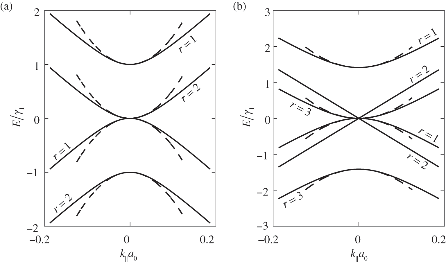
  values are positive and the other half are negative, there are N conduction bands and N valence bands. As an example, the band structure of AB-stacked bilayer graphene (
 ) is shown in Figure 1.8(a), where the solid curves are obtained from (1.58) without approximation and the dashed curves are obtained from (1.59) and (1.60) under the small-
 approximation, using
  and
and  obtained from experiments [Reference Abergel, Apalkov, Berashevich, Ziegler and Chakraborty4]. As can be seen, there are two bands for each value of r (marked next to the curves), and there are a total of
 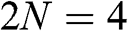 bands for the bilayer system, all of which are massive bands. The effective mass in the small-
 limit is
 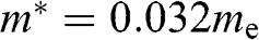 , where
 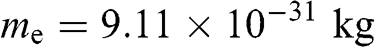 is the rest mass of a free electron. The eigenvectors can be obtained accordingly from (1.54) for
 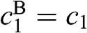 and
and  , which in turn give
  and
and  from (1.48):
  , where the eigenenergy E is given in (1.58).
For odd N, we can always find a value of r such that  given by (1.57), for which (1.58) gives the linear bands
  . Therefore, there are
  massive conduction and valence bands described by (1.59) and (1.60), and two linear bands defining one massless Dirac cone given by
  . As an example, the band structure of AB-stacked trilayer of
  is shown in Figure 1.8(b), where six bands can be seen; four are massive bands and two are massless linear Dirac bands.


From the above discussions, N-layer AB-stacked graphene has  bands. For even N, all
  bands are massive bands. For odd N, there are
  massive bands plus two massless linear Dirac bands.
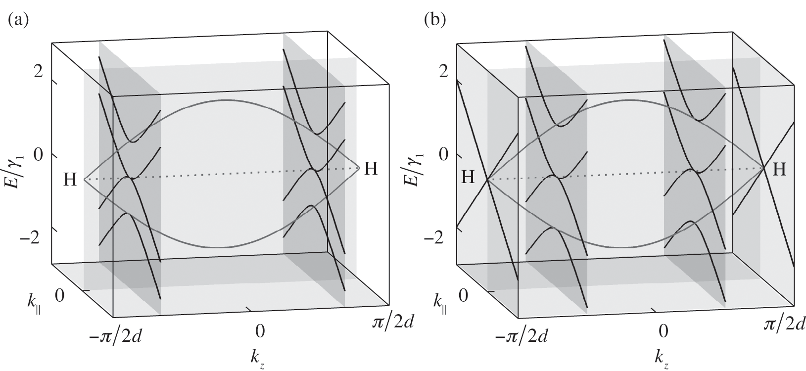
The band structure of natural graphite follows the AB stacking order; it can be obtained from (1.56) and (1.57) by taking the limit that  in (1.54). In this limit,
  is no longer discrete but forms a continuous spectrum. In a reduced Brillouin zone scheme,
  spans from
  to
to  , where the H point is located, as shown in Figure 1.9 [Reference Slonczewski and Weiss12]. At
  , there are three energy bands: one energy band for
  given by (1.50), and two energy bands for
  given by (1.57) with
  for a conduction band and
  for a valence band, as shown in Figure 1.9. By using (1.58), one can map out the band structure of graphite as a function of
  at different values of
  . The band structures of bilayer and trilayer graphene are shown in Figure 1.8. For bilayer graphene, two bands at
  , respectively, in the reduced zone scheme are shown in Figure 1.9(a). For trilayer graphene, the massive bands at
  and the massless Dirac bands at
  are also plotted, as shown in Figure 1.9(b). Note that the mirrored band structure does not represent double degeneracy because the positive and negative values of
  do not represent two independent eigenstates but represent two counter-propagating waves that form the standing wave in multilayer graphene. As can be seen from (1.54) and (1.56), for any solution of
  , the values of
  obtained using the positive and negative values of
  only differ by a negative sign. Therefore, both sets of the coefficients
  obtained from the positive and negative values of
  give the same eigenstate
  . The truly independent states are the standing waves of different wave numbers represented by different values of
  .
.

Figure 1.9 Band structures of AB-stacked (a) bilayer graphene and (b) trilayer graphene, obtained by cutting the band structure of graphite at certain  values.
1.6.2 AA Stacking Order
In the AA stacking order, the sublattice A of the upper layer is directly above the sublattice A of the lower layer, and the sublattice B of the upper layer is also directly above the sublattice B of the lower layer, as shown in Figure 1.10. Nearest-neighbor intralayer and interlayer interactions are considered. The intralayer interaction energy  and the interlayer interaction energy
  of AA-stacked multilayer graphene are not generally the same as
  and
and  of AB-stacked multilayer graphene.
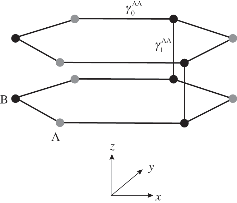
Figure 1.10 Atomic structure of AA-stacked bilayer graphene.
The tight-binding Hamiltonian at the  point for AA-stacked multilayer graphene is constructed as [Reference Min and MacDonald10]
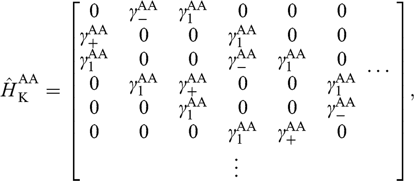 (1.61)
where  with
with  . The basis for
  is again taken to be
  , with the eigenvector
 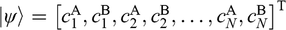 , both of which have the same form as those for
  of (1.47). By applying the eigenvalue equation
  , we find from (1.61) the following difference equations:
 (1.62)
 (1.63)
where  and
and  .
.
Now we want to transform (1.62) and (1.63) into a form similar to that of (1.53), whose solutions are already known. To do so, we first multiply (1.63) by an unknown variable x that gives us the freedom to adjust the coefficient. We then add (1.62) to (1.63). With some arrangements followed by collecting terms of the same n index, we get
 (1.64)
If  , which can be satisfied by taking
  , (1.64) can be simplified:
 (1.65)
where  . Equation (1.65) has the form of (1.53); therefore, we obtain the eigenenergies:
 (1.66)
where the identity  is used,
  is given by (1.56) with
  replaced by
  , and
, and  is the distance between two AA-stacked graphene layers [Reference Lobato and Partoens13,Reference Lee, Lee and Ahn14]. Different from the bands of AB-stacked multilayer graphene, the energy bands of AA-stacked graphene given in (1.66) are all massless linear bands. These linear bands form Dirac cones of shifted energies.
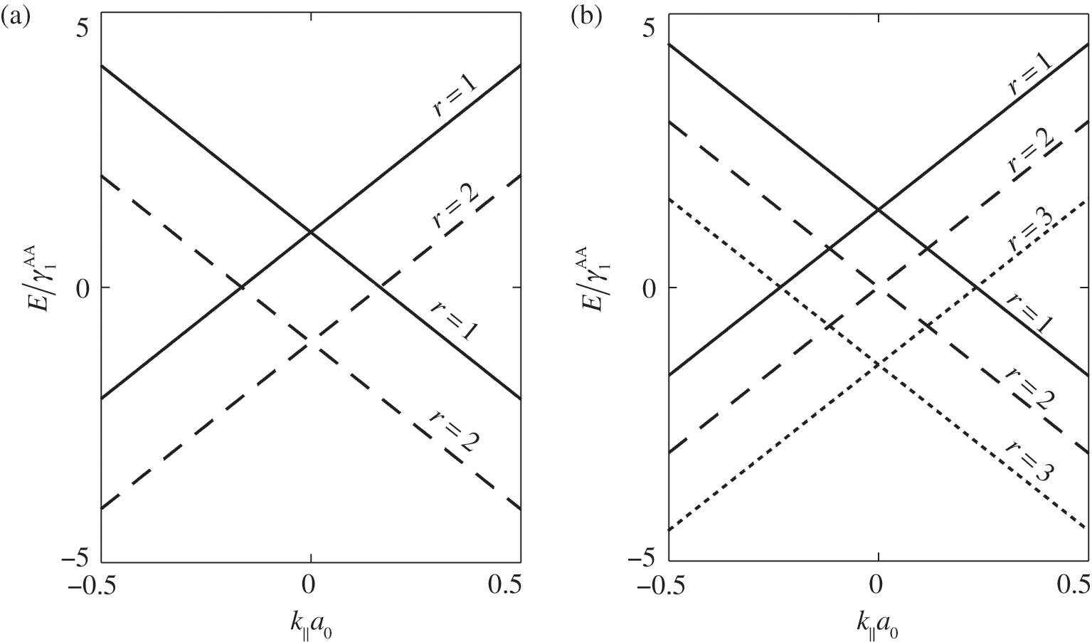
As examples, the band structures of AA-stacked bilayer graphene ( ) and trilayer graphene (
 ) are shown in Figures 1.11(a) and (b), respectively, using
  and
and  [Reference Lobato and Partoens13,Reference Lin, Liu and Shi15]. As can be seen, there are two bands for each value of r (marked next to the curves) and a total of
  bands for the system. The shift of the Dirac point for each band is determined by the second term in (1.66). Note that each Dirac cone of a given r value has its unique
  value. Therefore, unless an out-of-plane momentum is provided, carrier transitions between two different Dirac cones are forbidden.

Figure 1.11 Band structures of AA-stacked (a) bilayer graphene and (b) trilayer graphene.
1.6.3 Misorientation and Other Stacking Orders
For chemically deposited multilayer graphene, misorientation might happen among graphene layers [Reference Lin, Liu and Shi15,Reference Mele16]. When the relative rotation is small, large areas of locally AA-stacked and AB-stacked regions are formed, as shown in Figure 1.12 for misoriented bilayer graphene. In such a case, each of these regions can be locally treated as AA or AB stacking if the mean free path of the carriers is much smaller than the physical size of the region. Otherwise, one must identify the unit cell of the misoriented multilayer system and numerically calculate the band structure. It is found that while the energy band is still linear around the K point, the Fermi velocity is greatly reduced and therefore localization of electrons is possible in misoriented multilayer graphene [Reference Trambly de Laissardière, Mayou and Magaud17].

Figure 1.12 Misoriented bilayer graphene with locally AA-stacked and AB-stacked regions.
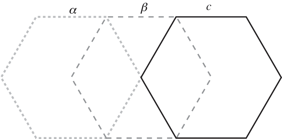
When the number of layers increases, the number of different possible stacking arrangements also increases. For example, in ABC-stacked multilayer graphene, there is a continuous, constant shift from one layer to the next, as shown in Figure 1.13.

Figure 1.13 ABC stacking of multilayer graphene formed by three distinct relative positions of graphene layers, labeled α, β, and c, each successively displaced by one carbon‒carbon distance.
The Hamiltonian of ABC-stacked graphene is given as
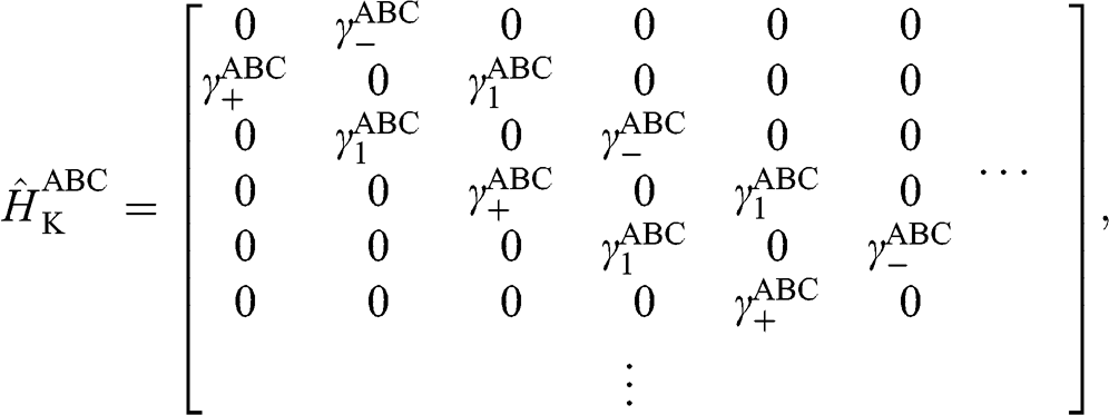 (1.67)
where  with
with 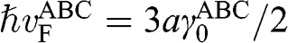 , and
, and  is the interlayer interaction energy. Again,
  is not generally equal to
  or
or  , and
, and  is not generally equal to
  or
or  [Reference Zhang, Sahu, Min and MacDonald18]. Simple as it might seem for the Hamiltonian shown in (1.67), there do not exist simple difference equations as those obtained for AB- and AA-stacked multilayer graphene [Reference Min and MacDonald10]. Instead, the eigenenergies of (1.67) are numerically obtained for the ABC trilayer and four-layer graphene, as shown in Figure 1.14. As can be seen, regardless of the number of layers, there are always two bands that touch at the K point. The other energy bands are shifted in energy and momentum in different manners but overlap at
  for
for  .
.
Figure 1.14 Band structures of ABC-stacked (a) trilayer graphene and (b) four-layer graphene.