0).
0).Introduction
Thin films incorporating GaN, InGaN and AlGaN are presently arousing considerable excitement because of their suitability for UV and visible light emitting diodes and laser diodes. However, the films are of variable quality because of the lattice mismatch between them and presently used substrates (sapphire and α-SiC). We are presently using a number of electron beam analysis techniques namely cathodoluminescence (CL) imaging, CL spectroscopy and electron backscattered diffraction (EBSD), to investigate both the structural and optical properties of nitride films in 3-dimensions. Information in the 3rd dimension is extracted by acquiring data at different electron beam energies. Electron beams of energy between 1 and 20 keV are well matched to the length scales typical of nitride heterostructures. For example, a 2 keV beam deposits energy to a depth of ≈50 nm, a 10 keV electron beam deposits energy to a depth of ≈ 600 nm, while a 20 keV beam deposits energy to a depth of ≈ 2 μm in a GaN layer.
In this paper we illustrate the application of electron beam techniques to the analysis of nitride thin films by presenting brief comparative studies of
-
(i) CL spectra of AlGaN and InGaN epilayers
and
-
(ii) EBSD patterns obtained from two silicon-doped 3 μm thick GaN epilayers grown on an on-axis (0001) sapphire substrate and a sapphire substrate misoriented by 10°toward the m-plane (10
0).
Experimental Details
All of the samples described in this paper were grown by metalorganic vapour phase epitaxy (MOVPE) on (0001) sapphire substrates (unless otherwise indicated). CL spectra were acquired using a home-built electron beam excitation system providing beams of energy up to 30 keV in a spot size of ≈ 200 μm at current densities up to 20 A cm−2 (but limited in the work to be described here to < 10 mA cm−2). In the present work the front faces of the samples were positioned normal to the exciting electron beam and CL detected from the sample edge. Samples were cooled to a temperature of approximately 25 K using a closed cycle helium cryorefrigerator. Spectra were acquired using an Oriel InstaSpecTM cooled 2-dimensional CCD array mounted at the output focal plane of a Chromex 0.5M monochromator.
A Cambridge 600S scanning electron microscope has been adapted by the addition of a home-built CL detection system (incorporating an Oxford Instruments parabolic mirror light collector) and a home-built EBSD imaging system. These allow the acquisition of comparative physical and luminescent images and EBSD patterns from the same area of a sample.
Experimental Results and Discussion
CL profiling of AlGaN and InGaN epilayer
A variable energy electron beam has been used to investigate an AlGaN-on-GaN bilayer, grown on a sapphire substrate. The thickness of the AlGaN and GaN layers were determined by Rutherford backscattering (RBS) to be 0.48 μm and 0.44 μm respectively, RBS measurements also revealed the mean aluminium concentration to be 7%.
Figure 1 shows low temperature CL spectra acquired from the AlGaN/GaN/sapphire layers at electron beam energies from 2 keV to 16 keV. Spectra have been normalised in intensity and shifted vertically for clarity. It can be seen that the highest energy CL emission band, which we attribute to bound exciton emission from the AlGaN, red shifts from 3.655 eV to 3.635 eV as the electron beam energy increases from 2 keV to 16 keV. No beam current dependence of this peak shift is observed. At electron beam energies ≥ 3 keV we observe a band peaking at ≈ 3.59 eV. This band increases in intensity with respect to the AlGaN bound exciton band as the electron beam energy increases. At electron beam energies ≥ 8 keV, an emission band at ≈3.475 eV becomes evident. We attribute this band to bound exciton emission from the underlying GaN epilayer. Also appearing at energies ≥ 8 keV is a shoulder on the high energy side of the GaN bound exciton band at ≈ 3.52 eV.
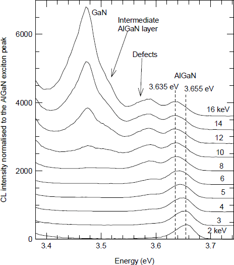
Figure 1 CL spectra acquired at different electron beam energies from an AlGaN/GaN/Sapphire structure.
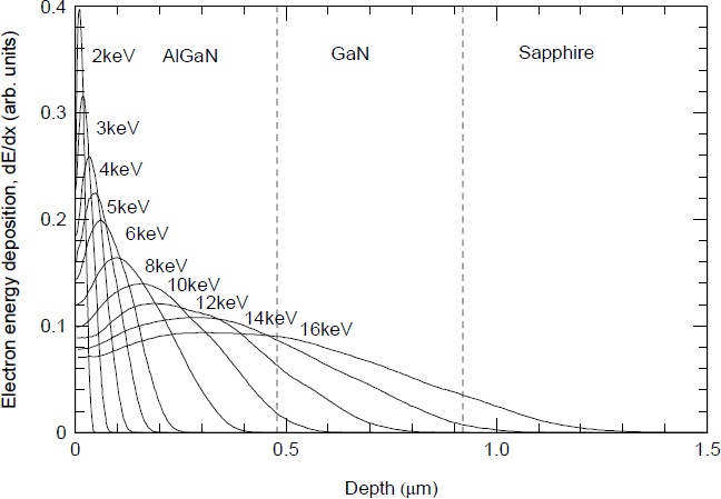
In order to interpret these results, it is necessary to know to what depth an electron beam of given energy penetrates the structure. Monte Carlo simulations of the electron trajectories [Reference Napchan, Holt and Cullis1] in an Al0.07Ga93N layer, were therefore carried out. Figure 2 shows the results of these simulations.

Figure 2. Electron beam energy deposition calculated using Monte-Carlo simulations of the electron trajectories in an Al0.07Ga0.93N layer.
Figure 2 illustrates that the electron beam penetrates deeper into the structure as its energy increases. It implies that electron beams with energy of 2 keV to 6 keV will address only the Al0.07Ga93N layer, while electron beams with incident energy ≥ 8 keV break through into the GaN underlying layer while electron beams with energy ≥ 14 keV penetrate the sapphire substrate. This explains why electron beam energies ≥ 8 keV are required to excite significant emission from the GaN underlying layer. Some emission is just discernible from the GaN layer at electron beam energies ≤ 8 keV, we attribute this to secondary excitation of the GaN by CL emission from the AlGaN layer.
With increasing energy, the electron beam will excite an increasing proportion of material near and at the interface between the AlGaN and underlying GaN layer. We might expect to observe emission associated with defects due to this interface. We attribute the peak observed at ≈ 3.59 eV to such defect emission, the intensity of this emission increasing with increasing electron beam energy as the electron beam excites higher proportions of defected material.
We propose that the shoulder on the high energy side of the GaN bound exciton band at ≈ 3.52 eV is due to an AlGaN layer with low aluminium concentration (≈ 2%) [Reference Steude2] at the interface between the AlGaN and GaN layers. We base this conclusion on the fact that this shoulder appears at the same electron beam energy as the GaN bound exciton band and must therefore occur at a similar depth in the sample as the top of the GaN layer. The intensity of the shoulder while similar to that of the GaN bound exciton band at 8 keV, drops to less than half the intensity of the GaN emission band at 16 keV. This reduction in relative intensity of the shoulder may be due to the absence of the source of this emission as the electron beam probes deeper into the sample, i.e., the shoulder emission at ≈ 3.52 eV is due to a thin sandwich layer.
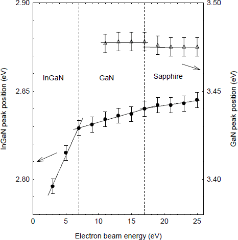
To understand the origin of the observed red shift of the AlGaN bound exciton band with increasing energy, we plot its peak position as a function of electron beam energy in figure 3. We also plot the dependence of peak position of the GaN bound exciton band. Figure 3 shows that the peak of the GaN bound exciton band shifts to the red by 15 meV as the electron beam energy is increased from 8 to 14 keV. These electron beam energies correspond to penetration depths of approximately 480 nm and 1.2 µm respectively, i.e., from the approximate location of the AlGaN/GaN interface to the GaN/sapphire substrate interface. We attribute this red shift to a relaxation towards the sapphire substrate of compressive strain in the GaN layer, where the strain is due to the overlying AlGaN layer. From the work of Kim et al [Reference Kim3] and Edwards et al [Reference Edward4], we estimate the change in stress across the GaN layer to be of order 4 kbar, this corresponds to a change in strain of approximately 0.15%. The AlGaN peak is seen to red shift by 20 meV as the electron beam energy is increased from 2 to 8 keV. These electron beam energies correspond to the electron beam penetrating from 50 nm to 480 nm into the layer, i.e., from close to the surface of the AlGaN layer to the AlGaN/GaN interface. As the electron beam energy increases from 8 keV to 16 keV the AlGaN peak continues to red shift as energy is deposited deeper into the sample. A total shift of 22 meV is observed. In this case there is more than one possible explanation for the red shift of the peak. It may be attributed to the relaxation towards the surface of the AlGaN layer of the tensile strain to which the underlying GaN subjects the AlGaN layer. Alternatively, the shift may be due to an increase in the aluminium concentration. A red shift of 22 meV from ≈ 3.65 eV corresponds to a change in aluminium mole fraction from ≈ 8% at the surface of the sample to ≈ 7% at the interface between the AlGaN and GaN epilayers [Reference Steude2]. It could be also due to a combination of a variation of strain and aluminium concentration. However, without an independent method of measuring either the strain or the aluminium concentration with a resolution of order 10 nm we cannot come to a definitive conclusion.

Figure 3. Shift of the peak of the AlGaN and GaN exciton peaks as a function of electron beam energy.
A variable energy electron beam has also been used to investigate an InGaN epilayer (≈ 400 nm thick) grown on an epilayer of GaN (1.0 μm), which in turn was grown on a sapphire substrate [Reference Trager-Cowan5]. Figure 4 shows the peak position of the InGaN emission band as a function of electron beam energy. We also plot the dependence of peak position of the GaN emission band. In this case there is no significant shift of the GaN peak position therefore no change in strain is detectable. The InGaN peak is seen to blue shift by 33 meV as the electron beam energy is increased from 3 to 7 keV. No beam current dependence of this peak shift is observed. These electron beam energies correspond to the electron beam penetrating from 90 nm to 350 nm into the layer, i.e., from close to the surface of the InGaN layer to the neighbourhood of the InGaN/GaN interface. As the electron beam energy increases from 7 keV to 25 keV the InGaN peak continues to blue shift as more energy is deposited deeper into the sample. A total shift of 50 meV is observed. As for the AlGaN epilayer discussed previously, there is more than one possible explanation for the observed blue shift. It may be attributed to the relaxation towards the surface of the InGaN layer of the compressive strain to which the underlying GaN subjects the InGaN layer. Alternatively, the shift may be due to an increase in the indium concentration towards the surface of the epilayer. A blue shift of 50 meV from ≈ 2.8 eV corresponds to a change in indium mole fraction from ≈ 15% at the surface of the sample to ≈ 14% at the interface between the InGaN and GaN epilayers [Reference O’Donnell6]. We have revised our values for the indium mole fraction from those published in [Reference Trager-Cowan5] in line with the results discussed in [Reference O’Donnell6]. The shift could also be due to a combination of a variation of strain and indium concentration. In this case we suggest that a change in indium concentration may indeed play a role. In [Reference Trager-Cowan5] we attributed the shift to the “compositional pulling effect” as reported by Shimuzu et al (1997) [Reference Shimuzu7] and Hiramatsu et al (1997) [Reference Hiramatsu8]. That is the indium mole fraction is observed to be low during the initial stages of InGaN growth on GaN epilayers, but increases with increasing film thickness. Again, as previously discussed for the AlGaN epilayer, without an independent method for measuring either the strain or the indium concentration with a resolution of order 10 nm we cannot come to a definitive conclusion as to the origin of the shift of the InGaN peak.

Figure 4. Shift of the peak of the InGaN and GaN emission peaks as a function of electron beam energy
EBSD patterns from GaN epilayers grown on misoriented sapphire substrates
EBSD is a diffraction technique that allows crystallographic information to be extracted from samples in a scanning electron microscope [Reference Dingley9]. In particular it allows the measurement of strain with a lateral spatial resolution of order 20 nm [Reference Dingley and Field10]. We present here some preliminary measurements from two silicon-doped 3 μm thick GaN epilayers grown on an on-axis (0001) sapphire substrate and a sapphire substrate misoriented by 10° toward the m-plane (10
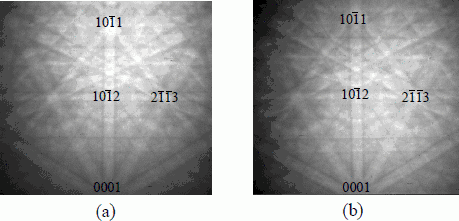
Figure 5. EBSD patterns from GaN epilayers grown (a) on and (b) 10° off-axis respectively.
A compression of the pattern towards the [1011] zone axis (pole) from the [0001] zone axis is observed in figure 5 (a) when compared to figure 5 (b). We tentatively attribute this shift to a difference of the in-plane compressive strain between the 2 samples where the 10° epilayer is under less compressive strain than the on-axis epilayer [Reference Troost11]. This result is consistent with those reported by Edwards et al [Reference Edward4] that GaN epilayers grown on vicinal substrates are less strained.
In the future we plan to quantify strain measurements using the EBSD technique. This will enable us to map the strain in GaN epilayers and will also allow us to make independent measurements of the strain in alloy samples such as the InGaN and AlGaN epilayers described in this paper. We may therefore come to definitive conclusions as to the origin of the observed shifts in the CL emission bands from these materials.