Introduction
“Superconducting artificial atoms” are electronic circuits comprising lithographically defined Josephson tunnel junctions, inductors (L), capacitors (C), and interconnects.Reference Clarke and Wilhelm1 Conceptually, they begin as linear LC resonant circuits (i.e., simple harmonic oscillators), which are then made anharmonic to varying degrees by adding a nonlinear inductive element, the Josephson junction (JJ) (see Figure 1). When cooled to dilution refrigerator temperatures (∼20 millikelvin), these superconducting circuits behave as quantum mechanical oscillators (e.g., “artificial atoms”) exhibiting quantized states of electronic charge, magnetic flux, or junction phase depending on the design parameters of the constituent circuit elements. Such superconducting artificial atoms have already proven to be a useful vehicle for advancing our general understanding of coherence, quantum mechanics, and atomic physics, particularly in regimes not easily accessible with natural atoms and molecules (for reviews, see References 1–6).
Superconducting qubits and their coherence. (a) The three fundamental superconducting qubit modalities: charge, flux, and phase. Each includes one or more Josephson junctions (shown in red). Illustration by Corey Reed, adapted from Reference 3. (b) The Josephson junction acts as both an inductor, L J, and capacitor, C J. External inductors and capacitors, L ext and C ext, can be added to modify the qubit’s potential energy landscape and reduce sensitivity to noise. (c) Because the Josephson junction inductance is nonlinear, the qubit potential is anharmonic. The qubit comprises the two-lowest states and is addressed at a unique frequency, f 01. (d) 15 years of progress in qubit coherence times, reminiscent of Moore’s Law for semiconductor electronics. On average, the doubling rate for coherence times in superconducting qubits is about once per year. Improvements have been driven by both new device designs and materials advances. Qubit modalities represented include charge,Reference Nakamura, Pashkin and Tsai8 quantronium,Reference Vion, Aassime, Cottet, Joyez, Pothier, Urbina, Esteve and Devoret9 flux,Reference Chiorescu, Nakamura, Harmans and Mooij83 2D transmon,Reference Houck, Schreier, Johnson, Chos, Koch, Gambetta, Schuster, Frunzio, Devoret, Girvin and Schoelkopf15 fluxonium,Reference Manucharyan, Koch, Glazman and Devoret84 and 3D transmonReference Paik, Schuster, Bishop, Kirchmair, Catelani, Sears, Johnson, Reagor, Frunzio, Glazman, Girvin, Devoret and Schoelkopf17 qubits.

The term “superconducting qubit” generally refers to the ground and first-excited state of a superconducting artificial atom. Due to the anharmonicity imparted by the JJ, the ground and first-excited states may be uniquely addressed at a frequency, f 01, without significantly perturbing the higher-excited states of the artificial atom. These two-lowest states thereby form an effective two-level system (i.e., a pseudo-“spin-1/2” system), and it is this degree of freedom that is used as the qubit, a quantum bit of information.
As quantum mechanical objects, superconducting qubits can be coherently controlled, placed into quantum superposition states, exhibit quantum interference effects, and become entangled with one another. The time scale over which a superconducting qubit maintains this type of quantum mechanical behavior, and thereby remains viable for quantum information applications, is generally called the “coherence time.” The rate at which the qubit loses coherence is related to its interactions with the uncontrolled degrees of freedom in its environment.
Within a standard (Bloch-Redfield) picture for spin-1/2 systems, there are two characteristic decay rates that contribute to coherence loss:
 $${\Gamma _1}\^{1 \over {{{\rm{T}}_1}}}$$
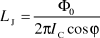
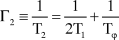 $${\Gamma _2} \equiv {1 \over {{{\rm{T}}_2}}} = {1 \over {2{{\rm{T}}_1}}} + {1 \over {{{\rm{T}}_\varphi }}}$$
The first is the longitudinal relaxation rate (energy decay rate) Γ1 = 1/T1, which characterizes the time T1 over which the qubit exchanges energy with its environment. Although T1 generally refers to both energy absorption and emission processes, for typical superconducting qubits, the qubit level splitting is generally much larger than the dilution refrigerator temperature, T (i.e., hf 01 >> k BT, where h is Plank’s constant and k B is the Boltzmann constant). Hence, the dominant T1-process here is energy emission to the environment coinciding with the qubit relaxing from the excited state to the ground state. The second is the transverse relaxation rate (decoherence rate) Γ2 = 1/T2, which characterizes the time T2 over which the device remains phase coherent; it is related to both the pure dephasing time Tφ (i.e., a blurring of the relative phase in a quantum superposition state) and T1 (i.e., losing the excited-state component of a quantum superposition state is a phase-breaking process).
Spectacular improvement in the capabilities of superconducting qubits over the past decade has brought these qubits from a scientific curiosity to the threshold of technological reality.Reference DiVincenzo7 (see Figure 1d and Figure 2) Many individual efforts contributed to this improvement, starting with the demonstration of nanosecond-scale coherence in a Cooper pair box (a charge qubit) by Nakamura and co-workers in 1999.Reference Nakamura, Pashkin and Tsai8 In 2002, Vion et al.Reference Vion, Aassime, Cottet, Joyez, Pothier, Urbina, Esteve and Devoret9 developed the quantronium qubit (a modified charge qubit) with a T2 coherence time of hundreds of nanoseconds based on the concept of design and operation at first-order noise-insensitive bias points. Burkard et al.Reference Burkard, Koch and DiVincenzo10 elucidated the importance of symmetry in qubit designs, which in conjunction with Bertet et al. brought persistent-current flux qubit coherence times into the few microseconds range.Reference Bertet, Chiorescu, Burkard, Semba, Harmons, DiVincenzo and Mooij11 In 2005–2006, Ithier et al.Reference Ithier, Collin, Joyez, Meeson, Vion, Esteve, Chiarello, Shnirman, Makhlin, Schriefl and Schon12 and Yoshihara et al.Reference Yoshihara, Harrabi, Niskanen, Nakamura and Tsai13 extensively measured the noise properties of quantronium and flux qubits, respectively, to better understand the sources of decoherence. The “transmon” qubit developed by Schoelkopf and co-workers significantly reduced the charge sensitivity of the Cooper pair box by adding a shunt interdigitated capacitor, which would later bring microsecond times to the cavity-QED (quantum electrodynamic) architecture.Reference Koch, Yu, Gambetta, Houck, Schuster, Majer, Blais, Devoret, Girvin and Schoelkopf14,Reference Houck, Schreier, Johnson, Chos, Koch, Gambetta, Schuster, Frunzio, Devoret, Girvin and Schoelkopf15 An MIT/NEC group increased T2 above 20 μs with a persistent-current flux qubit in a 2D geometry using dynamical decoupling sequences,Reference Bylander, Gustavsson, Yan, Yoshihara, Karrabi, Fitch, Cory, Nakamura, Tsai and Oliver16 and the 3D-cavity approach developed at YaleReference Paik, Schuster, Bishop, Kirchmair, Catelani, Sears, Johnson, Reagor, Frunzio, Glazman, Girvin, Devoret and Schoelkopf17 and now used by several groups has further increased this time to around 100 μs.Reference Rigetti, Gambetta, Poletto, Plourde, Chow, Corcoles, Smolin, Merkel, Rozen, Keefe, Rothwell, Ketchen and Steffen18 More recently, improvements in substrate preparation and materials choices, addressing issues elucidated by the 3D geometries, have led to improved coherence of 2D geometries.Reference Barends, Kelly, Megrant, Sank, Jeffrey, Chen, Yin, Chiaro, Mutus, Neill, O’Malley, Roushan, Wenner, White, Cleland and Martinis19,Reference Chang, Vissers, Corcoles, Sandberg, Gao, Abraham, Chow, Gambetta, Rothwell, Keefe, Steffen and Pappas20 This five-orders-of-magnitude improvement in the primary single-qubit metric can be justly termed a “Moore’s Law for quantum coherence,”Reference Steffen21 approaching levels required for a certain class of fault-tolerant quantum error correction codes.Reference Fowler, Stephens and Groszkowski22–Reference Fowler, Mariantoni, Martinis and Cleland24 In addition, the control of singleReference Lucero, Hofheinz, Ansmann, Bialczak, Katz, Neeley, O’Connell, Wang, Cleland and Martinis25–Reference Merkel, Gambetta, Smolin, Poletto, Corcoles, Johnson, Ryan and Steffen29 and coupledReference Yamamoto, Neeley, Lucero, Bialczak, Kelly, Lenander, Mariantoni, O’Connell, Sank, Wang, Weides, Wenner, Yin, Cleland and Martinis30,Reference Chow, Gambetta, Corcoles, Merkel, Smolin, Rigetti, Poletto, Keefe, Rothwell, Rozen, Ketchen and Steffen31 qubits has also advanced, with reports of gate fidelities as high as 99.85%.Reference Gustavsson, Zwier, Bylander, Yan, Yoshihara, Nakamura, Orlando and Oliver28,Reference Merkel, Gambetta, Smolin, Poletto, Corcoles, Johnson, Ryan and Steffen29
Electronic components and superconducting qubit circuits. (a) Schematic of a Josephson tunnel junction (JJ), with two superconducting electrodes separated by a very thin insulating barrier. (b) A JJ formed by double-angle shadow evaporation, where the overlapping layers are separated by the tunnel barrier. (c) Fabrication of a trilayer JJ (shown in transmission electron microscopy [TEM] image) by lithographic patterning and selective etching. (d) A parallel-plate capacitor with dielectric removed and (e) an interdigitated capacitor—both used as external capacitors (C ext) in qubits. (f) A NbN meander-wire inductor used as an external inductor (L ext) in a flux qubit.Reference Kerman, Dauler, Keicher, Yang, Berggren, Gol’tsman and Voronov85 Alternatively, a junction array may be usedReference Manucharyan, Koch, Glazman and Devoret84 (not shown). (g) Confocal optical image of a shadow-evaporated flux qubit and its readout superconducting quantum interference device (SQUID). (h) Co-planar waveguide (CPW) resonator, capacitively coupled to a microwave feed-line, used to control and readout a transmon qubit. (i) Scanning electron microscopy image of a flux qubit and readout SQUID parametric amplifier fabricated in a planarized trilayer process. Here, the wiring dielectric has been removed by wet-etching after device fabrication, resulting in suspended wires over bare Si substrate.Reference Yamamoto, Inomata, Watanabe, Matsuba, Myazaki, Oliver, Nakamura and Tsai86 All materials and devices were grown and fabricated at MIT Lincoln Laboratory.
There is a general consensus within the community that understanding and further mitigating sources of decoherence in superconducting qubits (Figure 3) is one key to more-advanced circuits and systems engineering. Indeed, coherence times should be made as long as possible, as exceeding the thresholds for quantum error correction will considerably reduce the resource requirements. Both T1 and Tφ are related to the environmental noise seen by the qubit, as characterized by a spectral density, S(f), and much is known about this noise. For example, inhomogeneous dephasing arises from broadband, low-frequency (e.g., 1/f-type) noise in the charge, flux, and critical current. However, although it is consistent with a bath of two-level fluctuators (or clusters of fluctuators), its microscopic origin is not yet well understood. Energy relaxation occurs due to noise at the qubit frequency, S(f 01), and design modifications can change the sensitivity of the device to this noise in ways that are understood. However, although several mechanisms are known to exist (e.g., coupling to microscopic defects), their origin is not well understood. Mitigating these types of decoherence mechanisms ultimately boils down to two general approaches: (1) reduce the qubit’s sensitivity to a given type of noise through design modifications; and (2) identify and reduce the sources of that noise through materials and fabrication improvements. In practice, the coherence improvements over the past decade were made through a combination of improved designs, improved fabrication, and improved materials. From this perspective, there remains an important role for materials and fabrication research in order to further improve qubit coherence times.
Illustration of various decoherence mechanisms that can affect superconducting qubits. The mechanisms include those related to materials and fabrication, as well as design and packaging considerations (environmental circuit modes and photons). Illustration by Corey Reed. Adapted with permission from Y. Nakamura.
The problem of materials-induced decoherence in superconducting qubits was recently reviewed by McDermott, where the physics of quantum decoherence and dephasing is discussed at a level beyond the scope of this review.Reference McDermott32 Here, instead, we aim to introduce the subject of materials in superconducting qubits. We introduce the basic qubit circuit elements (Figure 2), describe their role in the device, and discuss their sensitivity to materials. Due to this sensitivity, superconducting devices have enabled researchers to access and see experimentally the impact of material defects and impurities like never before (Figure 3). It has also pushed researchers to utilize alternative materials, develop new methods for their deposition, and incorporate them into new processes for fabricating devices. We hope to convey the important role materials science has already played in the community’s understanding of decoherence in superconducting qubits, and point out future directions in which new materials science is likely to have a large impact.
Josephson tunnel junctions and two-level systems
Josephson tunnel junctions are formed by two superconducting electrodes separated by a very thin (∼1 nm) insulating barrier. In this configuration, the collective superconducting order of one electrode (parameterized by a phase φ1) coherently connects with that of the other electrode (φ2) via the elastic tunneling of Cooper pairs through the barrier (see Figure 2). As Josephson first showed more than 50 years ago, the resulting supercurrent, I, and junction voltage, V, are related to the superconducting phase difference, φ = φ1–φ2, across the junction:Reference Josephson33
 $$I = {I_C}\sin \varphi$$
 $$V = {{{\Phi _0}d\varphi } \over {2\pi \,dt}}$$
Here, I C is the junction critical current, determined by junction area and barrier transparency, and Φ0 = h/2e is the superconducting magnetic flux quantum. Combining these using a standard relation for inductance, V = L J (dI/dt), one can identify a Josephson inductance,
 $${L_J} = {{{\Phi _0}} \over {2\pi {I_C}\cos \varphi }}$$
which is nonlinear in φ. The parallel-plate-like structure of the Josephson junction electrodes results in a self-capacitance, C J, which, when combined with the nonlinear L J, makes for an anharmonic oscillator (see Figure 1). It is this feature of the Josephson junction that can turn a harmonic superconducting circuit into a uniquely addressable qubit.
The most widespread and robust process for fabricating Josephson junctions involves the diffusion-limited oxidation of an aluminum base layer to form a relatively uniform amorphous oxide tunnel barrier.Reference Gurvitch, Washington and Huggins34 The process is widespread, despite the fact that for nearly 30 years this approach has been known to produce barriers with measureable densities of defects.Reference Rogers and Buhrman35,Reference Wakai and Van Harlingen36 These defects were thought to be either localized states in the insulator’s bandgap that can temporarily trap electrons, or as tunneling “hot-spots” that incoherently shunt the tunnel junction. Both mechanisms were thought to be responsible for 1/f -type noise (e.g., voltage noise across the junction or flux noise in a superconducting quantum interference device [SQUID]). These noise sources are now considered to be of secondary importance when compared with those defects that form microscopic two-level systems (TLSs).
In the context of superconducting qubits, a TLS is a localized low-energy excitation that is predominantly found in noncrystalline dielectric materials. Microscopically, a TLS is generally visualized as an ion or electron that can tunnel between two spatial quantum states. These systems occur due to either defects in the crystal structure or the presence of polar impurities such as OH–. Because of the charged nature of the TLS, it has a dipole moment that will interact with electromagnetic fields. Intentionally or otherwise, dielectric materials are found in every type of electronic device, and superconducting qubits are no exception. Because qubits operate at very low temperatures and powers, TLSs can significantly impact their performance.
The impact of TLSs on qubit coherence was not fully appreciated until the observation by Simmonds et al. in 2004 of individual spurious microwave resonators in a phase qubit.Reference Simmonds, Lang, Hite, Nam, Pappas and Martinis37 These resonators were observed in qubit spectroscopy measurements as avoided level crossings—the energy-level repulsion that occurs, proportional to the coupling strength, when two coupled quantum systems become degenerate (have the same energy splitting) and hybridize (see Figure 4c). These spurious resonators were observed to limit both the qubit’s coherence and measurement fidelity. Cooper et al. later used a similar device to demonstrate quantum-coherent oscillations between a qubit and TLS, and observed that the coherence times of a TLS could be comparable to (or even longer than) those of the qubits available at that time.Reference Cooper, Steffen, McDermott, Simmonds, Oh, Hite, Pappas and Martinis38 Shortly thereafter, Plourde et al. observed TLSs in a flux qubit.Reference Plourde, Robertson, Reichardt, Hime, Linzen, Wu and Clarke39
There are two primary ways by which a TLS in the tunnel barrier can interact with the qubit.Reference Ku and Yu40 In the first scenario, the dipole moment of the TLS couples directly to the voltage across the junction.Reference Martin, Bulaevskii and Shnirman41 When the TLS and qubit are in resonance, charge fluctuations in the former drive phase oscillations in the latter, and the two quantum systems become coupled. The qubit exchanges energy coherently with the TLS, which subsequently loses that energy via phonon emission, resulting in decoherence of the coupled qubit-TLS system. In the second scenario, low-frequency charge fluctuations in the TLS causes fluctuations in the height of the junction’s tunneling barrier.Reference Yu42 This modulation of the barrier height leads to critical current noise, which in turn produces fluctuations in the energy level splitting of the qubit and leads to dephasing. Based on the distribution of TLS-qubit avoided level crossings observed in phase qubits, Martinis et al. concluded that it was the direct interaction of the junction’s electric field with charge fluctuations that caused the spectral splittings.Reference Martinis, Cooper, McDermott, Steffen, Ansmann, Osborn, Cicak, Oh, Pappas, Simmonds and Yu43 That is not to say that critical current fluctuations will not matter, but experiments performed to date suggest they are not yet a limiting factor in measured qubit coherence times.Reference Van Harlingen, Robertson, Plourde, Reichardt, Crane and Clarke44
If TLSs exist in the thin insulating oxide that serves as the Josephson tunnel barrier, can they be eliminated, or at least drastically reduced, by improving the oxide quality? Oh et al. showed that, yes, their number can be reduced by growing a crystalline barrier layer.Reference Oh, Cicak, Kline, Sillanpaa, Osborn, Whittaker, Simmonds and Pappas45 In general, the conventional approach has been to oxidize the surface of a thin Al layer to form an amorphous AlOx barrier.Reference Gurvitch, Washington and Huggins34 In this process, the thickness of the oxide, and the critical current density of the resulting JJ, is determined by a combination of oxygen gas exposure and diffusion kinetics. In contrast, Oh et al. grew ultra-thin epitaxial Al2O3 layers on the (0001) surface of rhenium (chosen for its low free energy of oxidation and near-perfect lattice match with sapphire) and used these crystalline multilayers for qubit fabrication (see Figure 4). When compared with a traditional diffused AlOx barrier, the epitaxial barrier showed five times fewer TLSs for the same tunnel junction size.
Reduction in two-level system (TLS) density resulting from the use of epitaxial trilayers. (a) Process for the growth of Re/Al2O3/Al trilayers with the corresponding electron diffraction images. Epitaxial Re is first deposited at high temperature (850°C) on C-plane sapphire, followed by the reactive deposition of Al2O3 at room temperature. The oxide layer is crystallized by annealing the film to 800°C in an O2 background. Finally, a polycrystalline Al layer is deposited for the top electrode. (b) A cross-sectional schematic showing the various device layers. For phase qubit fabrication, the trilayer is patterned using standard photolithography and selectively etched. Amorphous SiO2 is used as an insulator, with vias etched to both the top Al electrode and the bottom Re electrode (red oval). A second Al layer is used to complete device wiring. (c) Spectroscopy scans from phase qubits with amorphous (top) and crystalline (bottom) tunnel barriers. By adjusting the bias current, one can change the operating frequency f μw of the qubit. The spectral splittings occur when the energy-level difference of the qubit matches that of a TLS in the junction barrier. The single-crystal barrier exhibits five times fewer such defects, with a resulting Rabi decay time of 90 ns. Reprinted with permission from Reference 45. © 2006 The American Physical Society.
Unfortunately, little progress has been made beyond this initial reduction in defect density. Instead of pushing for new materials that reduce TLS densities another order of magnitude or more, the superconducting qubit community has largely avoided the TLSs observed primarily in phase qubits (junction feature sizes 1–10 μm) by making qubit designs with smaller junctions (feature sizes 0.1–0.3 μm) and thereby reducing the net number of defects. In contemporary qubits, in fact, it appears anecdotally that the TLS defect density may actually decrease, speculatively due to reduced effects of stress in the smaller geometries. Indeed, there are reports of qubits featuring small junctions that exhibit very low-loss junction inductanceReference Bylander, Gustavsson, Yan, Yoshihara, Karrabi, Fitch, Cory, Nakamura, Tsai and Oliver16,Reference Paik, Schuster, Bishop, Kirchmair, Catelani, Sears, Johnson, Reagor, Frunzio, Glazman, Girvin, Devoret and Schoelkopf17 and junction capacitance.Reference Bylander, Gustavsson, Yan, Yoshihara, Karrabi, Fitch, Cory, Nakamura, Tsai and Oliver16,Reference Kim, Suri, Zaretskey, Novikov, Osborn, Mizel, Wellstood and Palmer87 Nonetheless, in the interest of long-term scalability, TLSs in the junction barrier should not be ignored. When scaled to the level of hundreds or thousands or even millions of JJs, and targeting high yield with minimal junction variation, it becomes clear that defect density (even a reduced one) will impact performance, and further work on tunnel barrier materials is warranted.
Some alternate approaches proposed by Welander et al. include a multilayer growth scheme for superconductor/insulator/superconductor “trilayers”Reference Welander46 and the growth of amorphous oxide barriers by co-deposition instead of diffusion.Reference Welander, McArdle and Eckstein47 The multilayer approach addresses the issue of high surface roughness in rhenium thin filmsReference Oh, Hite, Cicak, Osborn, Simmonds, McDermott, Cooper, Steffen, Martinis and Pappas48 by instead using rhenium as a buffer layer only between a thick, smooth bottom electrode layer (e.g., Nb) and a crystalline oxide tunnel barrier. On the other hand, a co-deposited amorphous oxide may also show reduced TLS density; Josephson junctions formed in this way exhibit near-ideal tunneling behavior, while those with diffused oxide barriers show an excess shunt conductance. Neither of these approaches has yet been reported to be utilized in a qubit.
For probing defects in tunnel barriers, Stoutimore et al. have developed a new device that is much simpler than a qubit in many respects: the Josephson junction defect spectrometer (JJDS).Reference Stoutimore, Khalil, Lobb and Osborn49 The JJDS is essentially a JJ in parallel with a meandering inductor and an inter-digital capacitor. Under an applied magnetic field, it becomes a frequency-tunable resonator with a nearly harmonic potential, which allows it to operate over a wide frequency range. The critical current of the JJ can vary by about a factor of 5 without affecting device functionality, and the only requirement for the JJ inductance is that it exceeds that of the parallel inductor. The JJDS is also compatible with both methods of JJ fabrication (shadow evaporation, and trilayer deposition and etching), making it a versatile device for the study of future tunnel junction materials.
What resonators can tell us about materials and fabrication
Resonators have been perhaps the most useful devices for the study of superconducting materials to date and have been used to identify a number of noise sources and decoherence mechanisms that affect qubits. Relatively easy to fabricate and measure, resonators have helped researchers characterize new materials and improve fabrication processes. This new knowledge has, in turn, played a large role in the ever-increasing coherence times of superconducting qubits.
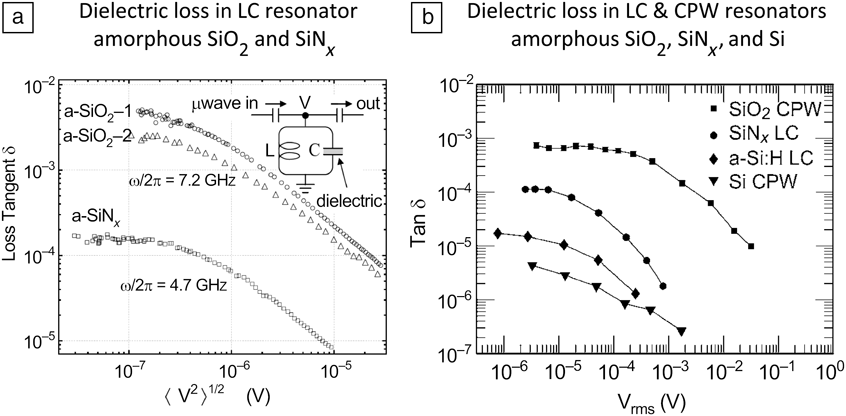
One application of resonators is in the detection of TLSs. Aside from appearing in the insulating tunnel barrier of a JJ, TLSs also reveal themselves in the dielectric materials used to separate and insulate between device wiring layers. An ensemble of TLS defects in these materials will absorb and dissipate energy at low powers and low temperatures, but will saturate as both voltage and temperature increase. This behavior will manifest itself as an increasing loss tangent, tan δ, with decreasing power that plateaus only at very low powers. In essence, at either high power (i.e., large ciculating field inside the resonator) or high temperatures, the TLSs saturate into a 50-50 mixture of ground and excited states. In this configuration, the TLSs exchange energy (absorb and emit energy) with both the resonator and the crystal lattice, thereby reducing the apparent energy loss from the resonator. In contrast, at low powers and temperatures that are cold compared with the TLS level splitting, the TLSs tend to be in their ground states. In this configuration, they can readily absorb energy from the resonator and dissipate that energy via phonon emission, thereby increasing the resonator loss. The low-power, low-temperature regime is of interest to qubits, because they operate at cold temperatures and low fields, generally absorbing or emitting only single photons when transiting between ground and excited states. This effect with TLSs was first observed by Schickfus and Hunklinger, who used a superconducting cavity resonator to measure the dielectric absorption of vitreous silica.Reference Schickfus and Hunklinger50 More recently, in the context of studying loss mechanisms relevant to superconducting qubits, Martinis et al. used a lumped-element LC resonator to measure the loss tangent of chemical vapor-deposited SiO2 and SiNx dielectrics at low temperature and variable power.Reference Martinis, Cooper, McDermott, Steffen, Ansmann, Osborn, Cicak, Oh, Pappas, Simmonds and Yu43 Both showed a decrease in tan δ with increasing power, but over the entire range studied, the SiNx loss was about 30 times lower (see Figure 5). A phase qubit was subsequently fabricated with SiNx and exhibited a coherence time about 20 times longer than that observed with SiO2 dielectric. Further resonator experiments by O’Connell et al. confirmed these findings and tested a number of other insulating materials, including bulk substrate crystals of silicon and sapphire.Reference O’Connell, Ansmann, Bialczak, Hofheinz, Katz, Lucero, McKenney, Neeley, Wang, Weig, Cleland and Martinis51 Using both CPW (co-planar waveguide) and LC resonators, they found that hydrogen-doped amorphous silicon (a-Si:H) showed a further fivefold improvement in loss tangent over SiNx.
Dielectric loss, tan δ, for several materials used in the fabrication of superconducting qubits. (a) A comparison of amorphous thin-film insulators grown by chemical vapor deposition, measured using an LC resonator with parallel plate capacitor. SiO2 was deposited from silane and oxygen precursors at two different temperatures: 13°C for a-SiO2-1 and 250°C for a-SiO2-2. SiNx was deposited at 100°C from silane and nitrogen. The lower tan δ for SiNx led to a 20-fold increase in T1. Reprinted with permission from Reference 43. © 2005 The American Physical Society. (b) Further comparison of dielectric loss, including hydrogen-doped amorphous silicon (a-Si:H) and bulk single-crystal CZ silicon. In this case, both lumped-element (LC) and co-planar waveguide (CPW) resonators were used for measurements. Again, amorphous silica exhibits the greatest loss, with a-Si:H loss nearly two orders of magnitude lower. Reprinted with permission from Reference 51. © 2008 AIP Publishing.
Resonators are also sensitive to the TLSs that form on metal surfaces and at interfaces between the metal and substrate. A number of research groups have studied CPW resonators fabricated from a variety of superconducting metals, including aluminum, niobium, and rhenium (see Figure 6a).Reference Gao, Zmuidzinas, Mazin, LeDuc and Day52–Reference Khalil, Wellstood and Osborn59 By measuring the loss (1/Q) and resonant frequency in these CPWs as a function of device geometry, power, and temperature, it is clear that TLSs are present. The primary culprit seemed to be native surface oxides that formed on the metal during air exposure. This argument was supported by the fact that CPWs made from niobium (a strong getter) had consistently higher loss than those made from either aluminum (oxide terminates at a few nm) or rhenium (very low free energy of oxidation).Reference Sage, Bolkhovsky, Oliver, Turek and Welander58 However, resonator electric-field simulations indicatd that the metal-substrate and substrate-air interfaces could dominate the surface loss.Reference Wenner, Barends, Bialczak, Chen, Kelly, Lucero, Mariantoni, Megrant, O’Malley, Sank, Vainsencher, Wang, White, Yin, Zhao, Cleland and Martinis88 With these results in mind, more recent work on resonator (and qubit) materials has centered on ways to either prepare the substrate better or use materials that are less susceptible to contamination in device processing or oxidation in air.
Using co-planar waveguide (CPW) resonators to compare materials and surface preparation techniques. (a) λ/2 resonators used in (b). (b) Comparison of resonator quality factor Q versus power (and average photon number) for CPW resonators fabricated from Al, Nb, Re, and TiN. Substrates, deposition technique, and metal crystallinity were varied with the following general trend: Nb exhibited the lowest Q, Al and Re were comparable, and TiN had the highest Q. See Reference 58 for details. (a–b) Reprinted with permission from Reference 58. © 2011 AIP Publishing. (c) Comparison of internal loss (1/Q) versus electric field for CPWs fabricated from TiN grown on sapphire, SiN films, and nitrided Si. At low fields (the regime of qubits), TiN growth on sapphire gave the highest loss, while that on bare silicon yielded the lowest-loss material. The substrate material and preparation procedure also impacted TiN film orientation. Reprinted with permission from Reference 62. © 2010 AIP Publishing. (d) Comparison of Q versus average photon number for Al CPWs on sapphire. Both the Al deposition technique (sputter, e-beam, molecular beam epitaxy [MBE]) and the substrate preparation method impact resonator quality, with about a fivefold variation in Q over the measured power range. In situ sapphire annealing at 850°C in an activated oxygen flux (O2*) gave the highest Q. Reprinted with permission from Reference 65. © 2012 AIP Publishing.
To address the issue of native oxides on metal surfaces, a number of groups have begun to fabricate CPW resonators from superconducting nitrides.Reference Sage, Bolkhovsky, Oliver, Turek and Welander58,Reference Barends, Hortensius, Zijlstra, Baselmans, Yates, Gao and Klapwijk60–Reference Vissers, Gao, Wisbey, Hite, Tsuei, Corcoles, Steffen and Pappas62 Titanium nitride (TiN) resonators have exhibited Q values that can be significantly higher than those for conventionally grown aluminum or rhenium. It has been suggested that this lower loss in TiN is because nitrides, in general, are very stable against oxidation. In fact, TiN has been shown to develop a surface oxide several nm thick after just one hour of air exposure.Reference Saha and Tompkins63 This is similar to the terminal oxide thickness on aluminum, so the improved Q values cannot be explained by a lack of surface oxide. Perhaps, by some unknown mechanism, the TiN native oxide simply has fewer TLSs than those on metals. Or, perhaps the difference is related to different etch chemistries, the metal-substrate interface that is influenced during the TiN growth, or some other fabrication-related loss mechanism.Reference Sandberg, Vissers, Kline, Weides, Gao, Wisbey and Pappas64
The substrate/superconductor interface is also critical to device performance.Reference Wenner, Barends, Bialczak, Chen, Kelly, Lucero, Mariantoni, Megrant, O’Malley, Sank, Vainsencher, Wang, White, Yin, Zhao, Cleland and Martinis88 Vissers et al. demonstrated this for TiN growth.Reference Vissers, Gao, Wisbey, Hite, Tsuei, Corcoles, Steffen and Pappas62 They found that careful cleaning of the Si wafer, followed by a brief nitridation of the Si surface just prior to TiN deposition, yielded CPW resonators with Q ∼ 106 at low powers (see Figure 6b). Films grown on sapphire or on thick SiN layers exhibited lower Q values—whether this was due to TLSs at the interface or in the thick SiN, or due to the observed change in film orientation is unknown. Regardless of the microscopic details, TiN has been successfully implemented in a transmon qubit, leading to measured coherence times (T1 and T2) of about 55 μs.Reference Chang, Vissers, Corcoles, Sandberg, Gao, Abraham, Chow, Gambetta, Rothwell, Keefe, Steffen and Pappas20 Megrant et al. found similar improvements for molecular beam epitaxially grown aluminum CPW resonators fabricated on sapphire wafers.Reference Megrant, Neill, Barends, Chiaro, Chen, Feigl, Kelly, Lucero, Mariantoni, O’Malley, Sank, Vainsencher, Wenner, White, Yin, Zhao, Palmstrom, Martinis and Cleland65 Prior to aluminum deposition at room temperature, the sapphire was either outgassed at 200°C in UHV, at 850°C in UHV, at 850°C in activated oxygen (O2*), or left untreated. Higher temperature heat treatments resulted in both better aluminum epitaxy and greater resonator quality factors, Q (see Figure 6c). The addition of O2* during outgassing improved Q for some devices, but did not impact others. Higher temperatures can serve to remove contaminants and recrystallize the substrate surface, and the O2* may be necessary to remove surface-bound elements like carbon and hydrogen. This cleaning procedure and epitaxial Al was incorporated into a modified transmon qubit that showed a significant increase in decay time (T1) up to 44 μs. With success stories like these, it is clear that much can be learned about superconducting materials and device fabrication through the study of resonators.
SQUIDs and flux noise
Excess magnetic flux noise has been a well-known problem in SQUIDs for more than 25 years.Reference Wellstood, Urbina and Clarke66 The noise spectrum at low frequencies scales approximately as A 2/(f/1 Hz), and the spectral density of the SQUID flux noise has decreased from approximately A = 10 μΦ0/Hz1/2 around 1990 to a level today of around A = 1 μΦ0/Hz1/2 at 1 Hz. This is generally attributed to improved fabrication processes. Aside from this general decrease, the observed 1/f behavior is nearly universal, having been observed by a number of research groups using a wide range of materials and device designs. Since SQUIDs are a primary building block of tunable superconducting qubits, it is perhaps not surprising that the influence of flux noise has also been observed in nearly all such qubits (e.g., see the flux noise characterization in References 13, 16, 67 [flux qubits], and 68 [phase qubits]). Recent measurements by Sendelbach et al. of SQUIDs at millikelvin temperatures showed them to be paramagnetic with a Curie-like 1/T susceptibility (see Figure 7a).Reference Sendelbach, Hover, Kittel, Muck, Martinis and McDermott69 This behavior, they argue, is the consequence of unpaired spins on the superconductor surface with an areal density of about 5 × 10¹⁷ m–2. (A similar density of spins has been observed on gold rings.Reference Bluhm, Bert, Koshnick, Huber and Moler70) Furthermore, these surface spins may interact and form spin clusters.Reference Sendelbach, Hover, Muck and McDermott71 Anton et al. observed a pivoting in the flux noise power spectra with temperature (see Figure 7b), and suggested that clusters can be either ferromagnetic, random (glassy), or antiferromagnetic.Reference Anton, Birenbaum, O’Kelley, Bolkhovsky, Braje, Fitch, Neeley, Hilton, Cho, Irwin, Wellstood, Oliver, Shnirman and Clarke72 While evidence of surface spins and their behavior on metals and superconductors is building, a precise understanding of their microscopic origin has been elusive.
Flux measurements using DC superconducting quantum interference devices (SQUIDs). (a) Paramagnetic behavior of surface spins in SQUIDs at millikelvin temperatures results in a change in the observed flux with temperature. Data for two SQUIDS are shown: one fabricated from a Nb-based trilayer, the other from an Al trilayer. The flux exhibits a Curie-type 1/T dependence. (b) The temperature-dependent flux through the Nb SQUID varies as a function of applied field, B fc, that is present as the Nb SQUID cools through the superconducting transition temperature. Also shown is the relative change in SQUID flux, ΔΦ, at temperatures between 500 and 100 mK versus the applied magnetic field during field cooling. (a–b) Reprinted with permission from Reference 69. © 2008 The American Physical Society. (c) Temperature dependence of flux noise spectral densities, S Φ(f) in two Nb trilayer SQUIDs. The top plot shows raw data for SQUID II.3, while the right plots show fits to A2/(f /1 Hz)α + C2, where α < 1. For both SQUIDs, the 1/f-type power spectra changes slope with temperature and generally pivots around a single frequency. Reprinted with permission from Reference 72. © 2013 The American Physical Society.
A number of theories have been put forth that attempt to explain the origin of these surface spins. Koch et al. suggested that the surface spins are unpaired electrons that hop between defect centers.Reference Koch, DiVincenzo and Clarke73 Hopping is thermally activated, and the electron spin is fixed in a specific orientation while it occupies the defect site. The spins of individual traps are randomly oriented, and the trapping energies vary broadly. A second model, proposed by Choi et al., involves potential disorder at the metal-insulator interface.Reference Choi, Lee, Louie and Clarke74 At an ideal, structurally coherent interface, there exist metal-induced gap states (MIGS) in the bandgap that extend into the metal but decay rapidly in the insulator.Reference Louie and Cohen75 A small amount of structural disorder will produce random fluctuations in the electronic potential, resulting in strongly localized, singly occupied MIGS near the interface. Both of these models—hopping spins and localized MIGS—presently involve independent spins, and it is not yet clear how to reconcile these with evidence of spin interactions and clustering.
Two models that include interactions have been proposed as well. Faoro et al. suggested that noise is produced by spins on the superconductor surface that are strongly coupled by Ruderman-Kittel-Kasuya-Yosida interactions.Reference Faoro and Ioffe76,Reference Faoro, Ioffe and Kitaev77 At intermediate frequencies, 1/f flux noise is due to spin diffusion, which is mediated by the exchange interaction with conduction electrons. Low-frequency noise, on the other hand, arises due to the slow switching rate of spin pairs between the singlet and triplet states. In the final model we present here, Wu and Yu have suggested that hyperfine interactions between electron spins on a metal surface and nearby nuclear spins are the source of 1/f flux noise.Reference Wu and Yu78 The surface electrons reside in harmonic traps and have relaxation times that are dominated by hyperfine spin exchange with the nearest non-zero nuclear moment. If this model holds, flux noise could be reduced significantly by switching to a superconductor with a low abundance of isotopes with nuclear moments. It should be emphasized, however, that none of these theories have been universally confirmed or refuted, and that more experimentation is needed to resolve this critical problem.
Summary
The past 10–15 years have witnessed coherence times in superconducting qubits increase dramatically—a full five orders of magnitude—bringing these devices to the threshold of technical reality. This evolution has been driven by innovations in qubit design, device fabrication, and materials science, and further research in these areas will be required to make superconducting qubit technology truly scalable. We have attempted to demonstrate how qubits and their constituent components have been useful in identifying previously unknown under-appreciated material defects, and how new materials and new fabrication processes can help improve device performance. Nowhere are these two sides of the coin more evident than with TLSs. Using qubits and resonators, one can observe the quantum behavior of individual TLSs and measure the loss stemming from TLS ensembles in dielectrics or on surfaces and at interfaces. New materials, growth procedures, and surface preparation methods have also eliminated many TLS sources, leading to substantial increases in resonator quality factors and qubit coherence times. One might hope that the same approach will help to elucidate and eliminate the source of interacting surface spins that seem to afflict both qubits and SQUIDs. And as the technology advances and superconducting qubits become more sensitive, the effects of decoherence mechanisms such as quasiparticle tunneling or critical current fluctuations are being revisited in more detail.Reference Pekola, Anghel, Suppula, Suoknuuti, Manninen and Manninen79–Reference Riste, Cultink, Tiggelman, Schouten, Lehnert and DiCarlo82 Moving forward, over the next decade, we anticipate a scaling in both the complexity and the requirements imposed on superconducting qubit circuits and their coherence times. Efforts to reduce the materials and fabrication-induced sources of decoherence will play an increasingly important role in maintaining and improving qubit performance in conjunction with these new engineering challenges.
Acknowledgments
The authors would like to acknowledge their colleagues at MIT Lincoln Laboratory, MIT campus, NEC, and the University of Tokyo, with whom they have had numerous fruitful discussions and collaborations related to the topics presented in this review.