Introduction
Recently, III-V nitride semiconductor lasers have been improved to the grade of a digital versatile disk (DVD) application. The multi-quantum-well (MQW) separated confinement hetero-structure (SCH) laser diodes have been realized to more than 10000 hours lifetime under continuous wave (CW) irradiation at room temperature (RT) [Reference Nakamura, Senoh, Nagahama, Iwasa, Matsushita and Mukai1]. The GaInN/GaN MQW laser diodes are the key devices for the realization of an advanced DVD system, therefore many groups have been developing intensively.
Akasaki, et al. reported for the first time all over the world the stimulated emission from AlGaN/GaN/GaInN quantum well device by current injection at RT in 1995 [Reference Akasaki, Amano, Sota, Sakai, Tanaka and Koike2]. After that, further progress has been achieved. The problem of high dislocation density was resolved by epitaxial lateral over-growth (ELO) GaN [Reference Usui, Sunakawa, Sakai and Yamaguchi3,Reference Nakamura, Senoh, Nagahama, Iwasa, Yamada, Matsushita, Kiyoku, Sugimoto, Kozaki, Umemoto, Sano and Chocho4] or pendeo-epitaxial growth [Reference Zheleva, Smith, Thomson, Gehrke, Linthicum, Rajagopal, Carlson, Ashmawi and Davis5]. In this way, the several developments were necessary for the improvements of laser diodes such as reduction of the threshold current and extension of lifetime under CW irradiation.
In this paper, we report the improvements of characteristics of the laser diodes by applying the reduction of internal loss at cavity and the multi low temperature (LT) buffer layers, the high power operation and a RT CW irradiation of the MQW-SCH laser diodes.
Experiments
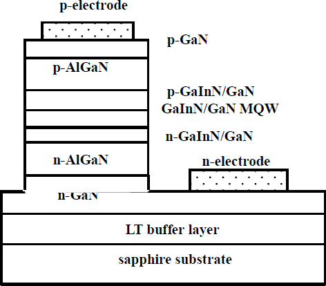
One of the schematic structures of GaInN/GaN MQW-SCH lasers is shown in figure 1. A LT buffer layer is grown on a-plane sapphire substrate. An n-GaN layer, an n-Al0.07Ga0.93N cladding layer, an n-GaInN/n-GaN optical guiding layer, a GaInN/GaN MQW active layer, a p-GaInN/p-GaN optical guiding layer, a p-Al0.07Ga0.93N cladding layer, and a p-GaN contact layer are followed. The MQW consists of 4 GaInN wells (1 to 4 nm) and GaN barriers (5 to 10 nm). The conventional optical guiding layers consist of GaN. However, we applied GaInN/GaN optical guiding layers, because an optical confinement factor of GaInN optical guiding layer is superior to that of GaN.
Schematic structure of the GaInN/GaN MQW-SCH laser diode on sapphire substrate.

Those GaN epitaxial layers are grown by metalorganic vapor phase epitaxy (MOVPE). The source gases of Al, Ga, In, and N are trimethylaluminum (TMA), trimethylgallium (TMG), trimethylindium (TMI), and ammonia (NH3), respectively. The dopant source gases of Si and Mg are silane (SiH4) and biscyclopentadienylmagnesium (bis-Cp2Mg). The growth conditions are the same as the previous report [Reference Koide, Kato, Sassa, Yamasaki, Manabe, Hashimoto, Amano, Hiramatsu and Akasaki6,Reference Akasaki, Amano, Murakami, Sassa, Kato and Manabe7]. Mg-doped p-AlGaN and p-GaN layers are activated by low energy electron beam irradiation after the growth. Dislocation density is evaluated by the method of KOH etch pit [Reference Kozawa, Kachi, Ohwaki, Taga, Koide and Koike8].
The laser diode is mesa geometry structure. The mesa widths are 2 to 5 µm, the cavity lengths are 300 to 700 µm, respectively. The mesa and the mirror facets are formed by reactive-ion-beam-etching (RIBE). TiO2/SiO2 dielectric multi layers are coated on both facets for the high-reflection (HR). From design, the reflectivity of a front and a back facets are 80% and 90%, respectively. The characteristics of the improved laser diode were measured under pulsed and CW current injection at RT. The pulse width was 100 ns and the duty ratio was 0.01%.
Results and Discussion
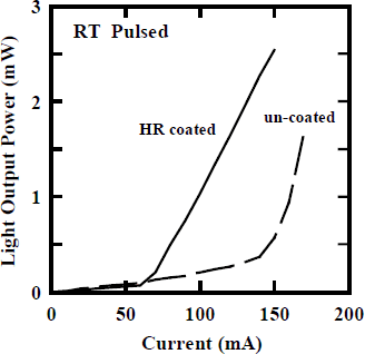
We introduced the GaInN/GaN guiding layers instead of GaN guiding layers to the conventional laser diodes and analyzed the internal loss [Reference Nakamura and Fasol9]. Therefore, the optical confinement effect was improved and the internal loss should be reduced. The internal loss was 25 to 30 cm−1 as same level as the mirror loss. The I-L-V characteristics of the HR coated laser diode under pulsed operation are shown in figure 2. The mesa width and the cavity length were 5 and 500 µm, respectively. The threshold current reduced from 140 mA (5.6 kA/cm2) to 60 mA (2.4 kA/cm2) by the HR facet coating.
I-V characteristics of laser diodes with HR coated and uncoated facets.
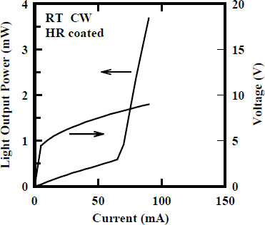
The CW irradiation of GaInN/GaN MQW-SCH laser diode was realized. The mesa width and the cavity length were 3 and 500 µm, respectively. The threshold current was 60 mA (4 kA/cm2) as shown in figure 3. The threshold current under CW irradiation is larger than that of pulsed operation due to thermal dissipation. RT-CW emission spectrum is shown in figure 4. The peak wavelength was 408 nm and its full width at half maximum (FWHM) was 0.03 nm.
I-L-V characteristics of GaInN/GaN MQW-SCH laser diode under CW irradiation.

Emission spectrum measured under CW irradiation.

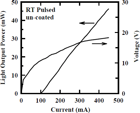
On the other hand, the highest power of the laser diode was 47 mW as shown in figure 5. The mesa width and the cavity length were 3 and 700 µm, respectively. This LD did not use the a multi LT buffer layers. The output power increased without saturation as a function of the current. Therefore, the laser diodes can write DVD sufficiently.
I-L-V characteristics of laser diode under high light output power operation.
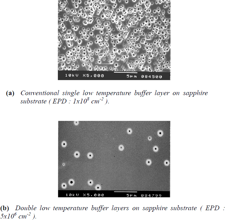
The multi LT buffer layers [Reference Iwaya, Takeuchi, Yamaguchi, Wetzel, Amano and Akasaki10] were effective for the reduction of dislocation. It is expected that a lifetime of blue laser diode can increase by reducing of defect. As shown in figure 6, the etch pit density (EPD) of 10 µm thickness GaN single layer surface using double LT buffer layers reduced from 1×108 cm−2 to 5×106 cm−2 . We applied the multi LT buffer layers to MQW-SCH laser diode epitaxial growth for the first time. The I-L-V characteristics of the laser diode using double LT buffer layers under CW irradiation is shown in figure 7. The mesa width and the cavity length were 3 and 500 μm, respectively. The threshold current was 64 mA (4.3 kA/cm2) and almost same as the result of using single LT buffer layer (figure 3). We have been optimizing the laser diode structure and investigating the lifetime.
SEM images of etch pits on GaN surfaces.
I-L-V characteristics of the laser diode grown on double low temperature buffer layer under CW irradiation.
Conclusion
We have succeeded in CW operation of GaInN/GaN MQW-SCH laser diode at RT. The high output power was more than 30 mW. The threshold current of 60 mA (4 kA/cm2) was achieved by introducing the GaInN/GaN optical guide layer. We have succeeded in applying multi LT buffer layers method to low defect density laser diodes for the first time.
Acknowledgements
The authors would like to acknowledge Professors I. Akasaki and H. Amano of Meijo University for helpful suggestions and discussions.