

1. Introduction
Because truly large single crystals of GaN have not yet been achieved for use as substrates, most GaN epitaxial growth and device research and development has relied upon hetero-epitaxial growth. The most common substrate currently used is sapphire, but LiGaO2 , ZnO, and SiC have also been tried Reference Doolittle, Kropewnicki, Carter-Coman, Stock, Kohl, Jokerst, Metzger, Kang, Lee, May and Brown[1] Reference Detchprohm, Amano, Hiramatsu and Akasaki[2] Reference Fischer, Wetzel, Hansen, Bourret-Courchesne, Meyer and Haller[3]. In order to obtain very low defect density GaN on sapphire and SiC, growth of thick films of GaN by HVPE Reference Molnar, Pankove and Moustakas[4], and innovations such as pendeo-epitaxy Reference Gehrke, Linthicum, Thomson, Rajagopal, Batchelor and Davis[5] Reference Zheleva, Smith, Thomson, Gehrke, Linthicum, Rajagopal, Carlson, Ashmawi and Davis[6] and Epitaxial Layer Overgrowth (ELO) Reference Parillaud, Wagner, Buehlmann and ILEGEMS[7], have been employed. Even with these additional processing steps, many defects remain which will reduce device yield and degrade device performance. Device cost will also be driven higher due to the larger number of processing steps required for device manufacture.
Growth of free-standing GaN bulk crystals has also been attempted. Square centimeter single crystal pieces have been obtained with ultra high-pressure growth Reference Grzegory, Bockowski, Lucznik, Krukowski, Wroblewski and Porowski[8]. Another approach has been to grow a thick gallium nitride film on a heterogeneous substrate such as SiC and then to remove the film from the substrate. This GaN film has less stress when the foreign substrate is removed at an elevated temperature and is thick enough to be used as substrate for epitaxial growth Reference Kelly, Vaudo, Phanse, Gorgens, Ambacher and Stutzman[9]. However, these growth methods may be of limited commercial value when producing large quantities of material. A third approach is to react gallium with gaseous ammonia to form GaN Reference Elwell, Feigelson, Simkins and Tiller[10]. This has always suffered from the problem of massive nucleation of very small crystals, usually smaller than 0.5 mm in diameter.
Several groups have used GaN substrates for homoepitaxy; the resulting films showed great improvement in quality Reference Foxon, Cheng, Korakakis, Novikov, Campion, Grzegory, Porowski, Albrecht and Strunk[11] Reference Kamp, Kirchner, Schwegler, Pelzmann, Ebeling, Lesczczynski, Grzegory, Suski and Porowski[12]. Thus, nitride devices made using films grown on single crystal GaN substrates should be superior to devices made using hetroepitaxial substrates.
In this article, we report a new method for growing nitride semiconductors, the chemical vapor reaction process (CVRP). The CVRP can be used to produce nitride single crystals, films, powders, and targets for sputter and pulsed laser deposition. We have grown GaN platelets as large as 2 mm × 9 mm × 100 μm at near-atmospheric pressures using this process, with growth rates up to 100 μm/hr in the hexagonal plane. We have achieved seeded growth in the c-direction, using previously grown c-plane platelets. During these synthesis and growth runs, uncontrolled nucleation is still a problem to be overcome.
2. Experimental
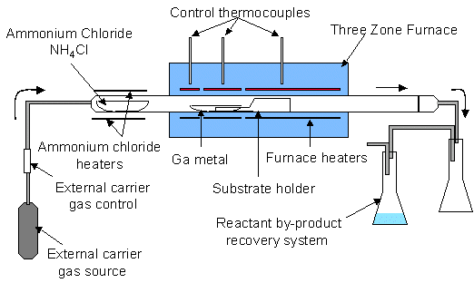
A Chemical Vapor Reaction Process (CVRP) apparatus is shown schematically in Figure 1. An ammonium chloride source (NH4Cl – 5-9s purity in powered form) sublimes upon heating in flowing carrier gas. The carrier gas flows into the main reaction chamber, which consists of a three-zone furnace, quartz reaction tube, and reactant recovery system. The three zones of the furnace allow for a temperature gradient between the gallium source and the substrate. By-products are captured in the recovery system downstream, consisting of a separation chamber to capture excess NH4Cl and other precipitants and a chamber containing water for scrubbing HCl, Cl2 , and NH3.
Schematic of a Chemical Vapor Reaction Process (CVRP) reactor.
In a typical experiment 60 grams of ammonium chloride and 40 grams of gallium are placed in their respective quartz boats. On several runs a quartz square with ~ 10 cm2 of surface area was placed on top of the substrate holder, located 1-10 cm downstream from the gallium. On some runs mm-size single crystal gallium nitride plates from previous runs were placed on the quartz substrate (see Figure 1). After the components are loaded and the reactor is assembled, a 3-5% hydrogen/nitrogen gas mixture is flowed at 225 sccm at room temperature into the quartz reaction tube (1.2m × 7cm dia.). While the system is being purged with forming gas, the temperature is increased, heating the gallium and substrate to the reaction temperature between 850 – 1050°C. Typical ramp time to temperature is 4 hours. The carrier gas continues purging at temperature overnight to remove oxides from the surface of the gallium and to rid the system of oxygen. After sufficient purging, ammonium chloride is introduced into the reaction zone by heating the NH4Cl source with an external heating jacket. The rate of nitrogen reactant delivered from the ammonium chloride is adjusted by controlling the temperature of the ammonium chloride and, to a lesser extent, by adjusting the flow rate of the carrier gas. Best results were obtained when the ammonium chloride was held at 225°C, where the vapor pressure is ~22 Torr. The flow rate of the carrier gas was maintained at 225 sccm throughout the experiment. The ammonium chloride typically flowed over the gallium for 24-48 hours. The entire experiment typically lasts 3 to 4 days.
During the course of the experiment, most of the gallium nitride forms on or slightly above the surface of the gallium in the boat as a somewhat spherical mass of polycrystalline GaN. Embedded within this mass are many small platelets of c-plane single crystal GaN. Figure 2 shows a polycrystalline mass after removal from the gallium boat.
Polycrystalline mass of GaN.

Seeded growth also resulted on the c-plates from previous runs. Surface properties of the c-plane platelets were analyzed by double axis x-ray rocking curve with a high-resolution four-circle x-ray diffractometer, Scanning Electron Microscope, and a high resolution Atomic Force Microscope. Powder diffraction, Glow Discharge Mass Spectrometry, and Inert Gas Fusion were performed to determine the purity of the platelets. Hall Effect and resistivity measurements were also performed.
3. Results
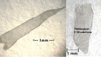
During the overnight purge with forming gas, the gallium remains in the boat and its surface is specular. But at the onset of the reaction between gallium and the nitrogen precursor the gallium surface becomes dull and a thin, polycrystalline crust forms. The crust may be mechanically tough and dense, with the interior containing numerous plate-like single crystals. On the upper surface of the crust, where the Ga vapor concentration presumably is low and the nitrogen precursor concentration is high, crystal growth is typically most rapid in the c-direction. Beneath the crust, where the Ga vapor concentration is high and the nitrogen precursor concentration is low because diffusion is inhibited, crystal growth is preferentially in the hexagonal plane, so wider c-plane platelets are formed. Usually no unreacted gallium remains in this polycrystalline mass at the conclusion of the experiment. However, if some does remain, it can be etched with a 50% by volume solution of nitric acid for 24 hours to aid in retrieving the single crystal platelets. Platelets as large as 9mm × 2mm × 100 μm have been retrieved. Figure 3 shows two representative platelets contained within the polycrystalline mass.
Single crystals of GaN plates. (c-direction is normal to platelet surface.)
The tendency toward c-direction growth increases on the crust near the edge of the quartz boat, where the nitrogen precursor concentration is presumably the highest and gallium concentration the lowest. A picture of some clearly defined c-axis growth on the edge of the crust is shown in Figure 4. This is similar to the results obtained in several other vapor transport systems for GaN growth Reference Elwell, Feigelson, Simkins and Tiller[10].
C-axis GaN growth on crust of polycrystalline mass.

A fraction of the gallium transports as vapor downstream from the gallium boat, forming gallium nitride on the quartz tubing. In this downstream region the c-axis growth habit is dominant, probably due to the gallium-deficient conditions. Thus, several experiments were performed by placing platelets from previous runs on the substrate holder located 1-10 centimeters downstream from the gallium boat in order to obtain seeded growth. Overgrowth of GaN on such c-plane seed platelets was successful, with an average growth rate of 20-25 μm/hr. The optical micrograph in Figure 5 shows the original seed crystal in the center and the rapid growth in the c-directions. Growth in the c+ direction was slightly faster than in the c- direction. Growth in the hexagonal plane was only ~ 20% as fast as along the C-axis. This type of preferential growth in the c-direction is typical for the gallium-deficient region in the CVRP growth system.
Nomarski micrograph of seeded GaN growth on c-plane.

4. Characterization
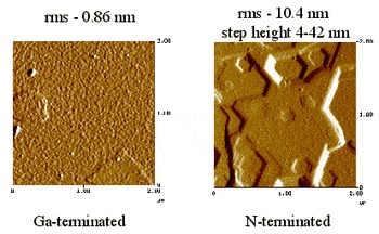
The GaN single crystals were clear and usually colorless. Visual inspection of the c-plane platelets shows one side has a specular surface while the other side does not. This morphology is similar to GaN single crystals grown by the high-pressure technique Reference Nowak, Krukowski, Grzegory, Porowski, Baranowski, Pakula and Zak[13]. Ponce et al. Reference Ponce, Bour, Young, Saunders and Steeds[14] determined that the specular side of the crystal was a Ga-terminated surface whereas the stepped side was N-terminated. We assume this is true of our crystals, also. Figure 6 displays AFM images of the surfaces of a GaN crystal platelet grown by CVRP. Steps 4.5 nm to 42 nm tall are clearly visible on the N-terminated surface. The Ga-terminated surface is featureless with a rms roughness of 0.86 nm, compared to a 10.4 nm rms for the N-terminated surface.
AFM images of (as grown) GaN platelet surfaces.
Powder diffraction indicates that the platelets shown in Figure 3 are pure gallium nitride. An x-ray rocking curve measurement performed on a Phillips high resolution five crystal diffractometer is shown in Figure 7. The measurement shows that the platelet is c-plane with a FWHM of 118 arc-seconds.
X-ray rocking curve of GaN single crystal platelet grown by CVRP.

The room temperature resistivity of a representative single crystal platelet was measured to be 0.323 ohm-cm, with Hall mobility of 103 cm2/Vs, and n-type carrier concentration of 1.93 × 1019cm−3. A calibrated SIMS measurement of the platelet material showed a very high concentration of oxygen (6 × 1020cm−3), which could explain the high carrier concentration. This was corroborated by inert gas fusion analysis, which revealed 0.142 percent oxygen (1.2 × 1020 cm−3). Glow Discharge Mass Spectrometry showed 1×1018 cm−3 silicon with all other detected elements present at less than 2.5 ppm. Chlorine was measured at 1.8 ppm.
5. Discussion
The following reactions occur upon sublimation of ammonium chloride Reference Smith and Calvert[15]
Only 4% of ammonia dissociates in the presence of quartz at 950°C Reference Smith and Calvert[15] and the dissociation of HCl is even slower Reference John and Jolles[16]. The ideal gas law can be used to determine the equivalent flow rates for HCl and NH3 gas when solid ammonium chloride sublimes. Thus, the equivalent flow rates from the resultant gases formed in the CVRP process for the experiments that were performed are approximately: 220 ccm N2, 7 ccm H2, 4-8 ccm HCl, and 3-6 ccm NH3 , with trace amounts of ammonium chloride and chlorine.
The mechanism for formation of GaN in the CVRP method is currently unclear because of the proximity of the ammonia and HCl when they react with the gallium. In a typical HVPE process, HCl flows over gallium to form gallium chloride (GaCl) at 800-900° C, which then combines with ammonia downstream (typical flow rates are 10-40 ccm for HCl and 300-1000 ccm for NH3 ) at 900-1100° C to form gallium nitride on a substrate Reference John and Jolles[16]. In CVRP the NH3 and HCl crack approximately at the same time and at a much lower NH3/HCl ratio than in a typical HVPE process (CVRP ~ 1:1, HVPE > 30:1). Since the NH3 and the HCl coexist in the same gas stream, a large percentage of gallium nitride is then immediately formed when these gases flow over the surface of the gallium in the hot zone.
It was desired to increase the NH3/HCl ratio in CVRP for a direct comparison with HVPE growth. We performed several CVRP experiments with ammonia added to the gas upstream of the ammonium chloride in order to increase the NH3/HCl ratio. This suppressed the sublimation of the ammonium chloride by reducing the HCl partial pressure (See Equation (1)). We plan additional experiments in which NH3 will be added downstream of the ammonium chloride to produce a higher NH3/HCl ratio without suppressing ammonium chloride sublimation.
Hoping to slow down nucleation, we used the CVRP method with ammonium bromide instead of ammonium chloride in one experiment, with limited success. The high temperature (800-900°C) of the growth zone may have prevented formation of GaN when ammonium bromide was used. The effect of various ammonium halides (NH4Cl, NH4Br, and NH4I) and their combinations will be studied in the near future.
The effect of carrier gases on the growth rate and morphology of GaN has been studied by several researchers. Molnar et al. found improved material quality and reduced growth rates when additional HCl was added to the flow downstream from the gallium source in HVPE systems Reference Molnar, Aggarwal, Liau, Brown, Melngailis, Gütz, Romano and Johnson[17]. Hydrogen and nitrogen are also said to have an influence on growth. Rebey et al. showed that increased hydrogen enhances GaN decomposition by gallium surface desorption above 830° C at atmospheric pressure, while nitrogen and ammonia suppress decomposition Reference Rebey, Boufaden and El Jani[18]. Koleske et al. showed that H2 pressure also affects decomposition Reference Koleske, Wickenden, Henry, Twigg, Culbertson and Gorman[19]. Thus, it is evident that decomposition reaction routes play a large role in changing the overall growth kinetics. This seems to be the case in the CVRP system because GaN formation is greatly reduced at temperatures above 1200° C, which might in part result from the equilibrium being shifted from GaN formation to GaN decomposition.
The constant reflux of growth could be one of the reasons why a large number of nucleation sites and crystallographic orientations of GaN result from vapor reactions. The equivalent gallium and nitrogen vapor pressures during the formation of GaN also have an effect on crystal morphology, as seen from the results in both the CVRP and other GaN growth processes Reference Grzegory, Bockowski, Lucznik, Krukowski, Wroblewski and Porowski[8] Reference Elwell, Feigelson, Simkins and Tiller[10]. In CVRP, the gallium and nitrogen vapor pressures are functions of both the intermediate compounds present and of the change in flow and diffusion conditions during the formation of the GaN crust. The formation-decomposition mechanism and the gallium and nitrogen vapor pressures may both influence nucleation and growth.
Oxygen and other contaminants also could affect growth mechanics. Chu et al. grew gallium nitride by flowing ammonia over gallium suboxide at 1150° C Reference Chu, Ito, Smeltzer and Chu[20]. Larger crystals resulted when gallium was added to the gallium suboxide. Kuznetsov et al. showed that trace amounts of oxygen and water caused formation of β-GaN during post-growth processing of HVPE-grown GaN Reference Kuznetsov, Rakova, Lee and Chong[21]. It is not as yet known how or whether oxygen influences the growth of CVRP GaN crystals before, during, and after sublimation of ammonium chloride is initiated.
Oxygen is probably the major factor in the high carrier concentration (>1019) in our CVRP GaN samples. This is undesirable for device applications.In our experiments oxygen could be introduced when the ammonium chloride, which is hygroscopic, is briefly exposed to air before loading, even though the ammonium chloride is purged with forming gas at ~ 150°C before being raised to sublimation temperatures. A small quantity of impurities could also come from the recovery system or outside the furnace by back-diffusion. Silicon contamination could be coming from the gallium metal. Finally, a small percentage of the concentrations of silicon and oxygen found in the CVRP crystals might have come from the quartz tube used in the growth chamber. The CVRP furnace will be redesigned to reduce the oxygen and other impurities in order to obtain crystals with smaller carrier concentrations.
In order to grow large bulk crystals, the kinetics of the system must be controlled. One of the main problems of growing bulk GaN at a high rate is the difficulty in containing the formation of GaN to a small reaction zone because of the growth reflux mentioned above. Successful transport processes for production of bulk crystals result when equilibrium of the growth reactions can be confined to a small temperature zone. A number of parameters influence the reaction rate between the reactant gases derived from ammonium chloride and the gallium metal in the CVRP. These include temperature gradient, exposed surface area of the gallium metal, the amount of ammonium chloride entrained in the carrier gas stream, growth and decomposition kinetics, and impurities such as oxygen. The thermodynamics and transport mechanism of gallium with the reactant gases in the hot zone is currently being investigated to increase crystal size and reduce the number of nucleation sites.
6. Summary
A new process for synthesis and growth of GaN single crystals by a chemical vapor reaction process (CVRP) has been described. The CVRP is distinguished by simplicity of design, low process temperatures and pressure, and abatement of toxic chemicals. Growth rates for GaN platelets were 25-100 μm/hr in the a-direction. Single crystal c-plane platelets of 9mm × 2mm × 100 μm thick were obtained by the process. Seeded growth in the c-direction with a growth rate of 20-25 μm /hour was also accomplished by re-growth on previously grown c-plane material. The platelets were single crystals of high purity material, with the exception of oxygen and silicon. A representative crystal had shallow donor doping concentration of ~ 2 × 1019 cm−3, roughly consistent with the oxygen concentration.
The authors thank AFRL-Sensor Directorate colleagues Sheng-Qi Wang for the x-ray rocking curve measurements, Pearl Yip for AFM measurements, Alvin Drehman for x-ray powder diffraction measurements, Michael Alexander for unwavering support and critical readings of manuscript drafts, and Gerald Iseler for technical discussions. David Look of Wright State University, James Solomon of the University of Dayton Research Institute, Dayton Ohio, and Rex Jones and Adam Saxler of the Air Force Research Laboratory, Materials and Manufacturing Directorate, Wright-Patterson Air Force Base, Ohio, provided additional characterization. This work was sponsored in part by the Air Force Office of Scientific Research (Gerald Witt and Maj. Dan Johnstone, program managers).


