

1. Introduction
In recent years, GaN has attracted the attention of numerous research groups due to its high potential for optoelectronic and high-power electronic applications. Reference Nakamura, Senoh, Nagahama, Iwasa, Yamada, Matsushita, Kiyoku and Sugimoto[1] Properties such as wide direct band gaps and high thermal stabilities make nitride semiconductors the superior material for laser diodes and laser emitting diodes in the blue and ultraviolet wavelength regions, as well as for devices operating at high temperature. Reference Amano, Kito, Hiramatsu and Akasaki[2] Epitaxial film quality with low defect density is of great importance for the success of all devices. Consequently, reducing the dislocation density is one of the key issues in obtaining better device performance. A remarkable reduction in the threading dislocation density has been obtained in several efforts by means of growth at high pressure/temperature using the hydride vapor phase epitaxy method (HVPE). Reference Teisseyere, Perlin, Suski, Grzegory, Porowski, Jun, Pietraszko and Moustakas[3] Reference Usui, Sunakawa, Sakai and Yamaguchi[4] Reference Kim, Lee, Moon, Hong and Yoo[5] Reference Park, Park and Choh[6]
Many researches have been carried out to analyze the characteristicss of dislocations in GaN films. Transmission electron microscopy (TEM), despite the extensive and skillful sample preparation it demands, is the general means to observe dislocation densities and structures. Reference Romano, Krusor and Molnar[7] Wet-chemical etching is a commonly used technique for surface defect investigation. Reference Rosner, Carr, Ludowise, Girolami and Erikson[8] Reference Minsky, White and Hu[9] Youtsey and co-workers demonstrated a photoenhanced electrical chemical (PEC) etching process that produces highly anisotropic “whisker-like” features in n-type GaN films. Luminescent radiators have also been used to estimate the dislocation's influence on device reliability for high current density conditions in III-V and II-VI materials. Rosner et al. showed, by the comparison of atomic force microscopy (AFM) and cathodoliminescence (CL) images, that the dislocation in GaN is a non-radiative recombination center. Reference Youtsey, Romano and Adesida[10] Nagahama found that the lifetime of the laser diodes (LDs) is strictly dependent on the dislocation densities of GaN substrates as revealed by dark spots in cathodoluminescence (CL) images. Reference Nagahama, Iwasa, Senoh, Matsushita, Sugimoto, Kiyoku, Kozaki, Sano, Matsumura, Umemoto, Chocho and Mukai[11]
We have recently demonstrated freestanding GaN films, 300 μm-thick GaN films with 2 inch size, grown by HVPE on sapphire substrates. Reference Park, Park and Choh[6] The dislocation density in these films, measured by TEM, was found to be on the order of 107cm−2. In this study, we describe an effective and accurate process enabling measurement of the dislocation density in GaN thick films using a micro photoluminescence (PL) method. We also performed homoepitaxial growth of GaN films with 500 and 750 μm thickness despite the small and cracked size. From the results of their dislocation densities., we have determined the relationship between the thickness and the dislocation densities of the GaN films.
2. Experimental
The GaN samples were grown on (0001) sapphire substrates using horizontal type hydride vapor phase epitaxy The growth of GaN was carried out under atmospheric pressure using nitrogen as the carrier gas. Ammonia gas (NH3) and HCl gas/Ga metal were used as nitrogen and gallium sources, respectively. Hydrogen chloride gas was supplied to Ga metal to form GaCl, which reacted with NH3 in the growth region between 1000 to 1050 °C, resulting in GaN formation on the sapphire substrates. The growth rate of GaN was approximately 30 ~ 100 μm /h under these conditions. The 300 μm thick GaN film was obtained without cracks and UV laser induced lift-off was employed to make a freestanding GaN substrate through separation of the GaN films from the sapphire. TEM, EPD, and a micro-PL measurements were then used to analyze the dislocation density. In order to investigate the correlation between the GaN film thickness and dislocation density, homoepitaxial GaN thick films, 500 and 750 μm thick, were grown on freestanding GaN substrates with a size of 10 x10 mm2. Their dislocation densities were measured using micro PL, which is a nondestructive method for measuring dislocations which cause the non-radiative recombination centers. Micro PL measurements were performed at room temperature using a He-Cd laser emitting at 325 nm. The corresponding excitation density was about 100 kW/cm2. The scattered light is dispersed by Yvon monochrometer and the optical signal was recorded by a photomultiplier (GaAs chip).
3. Results and Discussion
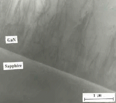
Figure 1 is a cross-sectional TEM image showing the grown region near the interface in a 300 μm thick GaN film grown by HVPE. It can be clearly seen that many dislocations originating from threading dislocations in the substrate GaN layer occurred within 1-2 μm of the film/substrate interface. From TEM analysis, the defect density of the 3 μm thick GaN film grown using the HVPE method was determined to be higher than 109 cm−2 . Figure 2a2ab shows a plan-view TEM image of the dislocation density at the GaN surface of the 300 μm thick film. Its threading dislocation density was estimated as to be approximately 1 × 107 cm−2 . Although the plane view TEM study was used to quantify the threading dislocations at the GaN surface, this method may be uncertain and has difficulty observing the number of threading dislocations in thick GaN films of high quality due to the small area measured. For more effective and accurate estimation of the dislocation density of GaN thick films having low defect densities, we used the wet chemical etching and micro photoluminescence analysis methods. Wet chemical etching is a commonly used technique for surface defect observation. Among the various etchants for GaN films are hot phosphoric acid (H3PO4), mixed H3PO4/H2SO4, and molten potassium hydroxide (KOH). We carried out etching at 220 °C using H3PO4 solution until the defects on the surface were clearly apparent as hexagonal pits. Figure 2b illustrates the GaN surface morphology produced by the etching process after 1 min of etching. The dislocations in the GaN film were uniformly distributed. The density estimated by counting the etch pits in several places is approximately 9 × 106 cm−2 , which is quite close to the result from TEM.
TEM image of the film/substrate of a 300 μm thick GaN film grown by HVPE.
Images of a 300 μm thick GaN film grown by HVPE. (2a, left) TEM of GaN surface, (2b, right) EPD.

Figure 2c shows a result of micro PL from the GaN film surface. The bright spots in the image represent high PL emission intensity, and dark spots represent low intensity. The bright and dark spots are distributed relatively uniformly over the whole area. The spots in the micro PL image were found to be spatially well resolved. In the image, the dark spots due to non-radiative recombination show a low PL intensity corresponding to dislocation sites. The estimated dislocation densities resulting from counts of the dark spots in the measured area were in the range of 7 × 10⁶to 1 × 107cm−2. As with TEM results, there was only a small deviation of the dislocation density with the measured position. This result shows that the micro PL measurement can be used for estimating the dislocation densities.
Micro PL for the 300 μm thick GaN film grown by HVPE

The dislocations in GaN films have edge, screw, or mixed characters but the origins of these threading dislocations are not well understood. Many of the threading dislocations are not perpendicular to the surface. Therefore, the defect reduction can occur with increasing film thickness, and the dislocation density changes. Reference Romano, Krusor and Molnar[7] In order to investigate the reduction of the dislocation density with the GaN film thickness, we performed normal growth, which does not use special growth techniques for reduction of the dislocation density such as selected area growth (SAG) or epitaxial lateral overgrowth (ELO). The freestanding GaN film was used for re-growth. Figure 3 show the micro PL maps revealing the dislocation density of the GaN films with a variation of the film thickness. In the case of a 3 μm thick film, as shown in Figure 3a, the dark spots observed at the GaN surface were uncountable and undistinguished. The average dislocation density estimated from TEM was higher than 1 × 109cm−2, which is similar to other research results. Figure 3c and Figure 3d illustrate the result for homoepitaxial GaN thick films grown on freestanding GaN substrates. As shown in Figure 3c, the dark spots were clearly apparent and their number decreased to about half compared to Figure 3b. Therefore, the dislocation density of the 500 μm thick GaN film was estimated at about 5 × 106cm−2. In contrast with Figure 3c, the micro PL map for a 750 μm thick GaN film, shown in Figure 3d, was not clear due to the degraded GaN surface with large hillocks and cracks, because the homoepitaxial growth was not performed in the optimum condition. However, it was possible to count the dark spots and the estimated dislocation density was about 2−3 × 106cm−2. This also shows half the dislocation density as compared to 500 μm thick GaN film. Thus, these results suggest that the threading dislocation density in HVPE GaN can be reduced by about half by increasing the film thickness by 250 μm. Based on the results of micro PL measurement, we plotted the correlation, shown in Figure 4, between the thickness and the dislocation densities of GaN films grown by HVPE. Although it is not yet known for certain how much dislocations should be reduced to apply GaN-based short wavelength laser diodes as light sources for digital versatile disks, a low defect density substrate is necessary. From the above results, it would be possible to forecast the defect reduction of GaN substrate grown by HVPE as an thickness increment.
Micro PL mapping images of the dislocation density of GaN films with the variation of thickness. (3a, left) 3 μm GaN film, (3b, right) 300 μm GaN film

Micro PL mapping images of the dislocation density of GaN films with the variation of thickness. (3c, left) 500 μm GaN film, (3d, right) 750 μm GaN film

Correlation between the thickness and the dislocation density of GaN films grown by HVPE on sapphire substrates

4. Conclusion
In summary, we have investigated the dislocation density of GaN films grown by hydride vapor phase epitaxy (HVPE) on c-plane sapphire substrates. Micro PL mapping is a nondestructive method for observing defect sites as dark spots, which provides strong evidence for non-radiative recombination occurring at the dislocations in GaN film surface. The number of dark spots, revealing threading dislocation sites, decreases with increasing thickness of GaN films. From the results of the micro PL mapping, it is possible to estimate the correlation between the thickness and the dislocation density of GaN films.
ACKNOWLEDGMENTS
The authors would like to thank Dr. Moonsuk Sun and Jaehee Cho at Samsung Advanced Institute of Technology for their support of this paper.


