

1. Introduction
GaN and related alloys are finding application for fabrication of blue/green/UV emitters (light-emitting diodes and lasers) and high temperature, high power electronic devices Reference Pearton[1] Reference Pankove and Moustaka[2] Reference Morkoc[3] Reference Nakamura and Fasol[4]. The emitter technology is relatively mature, with light-emitting diodes being commercially available since 1994 and blue laser diodes also available from Nichia Chemical Industries. Electronic devices such as heterostructure field effect transistors (FETs), heterojunction bipolar transistors (HBTs), metal oxide semiconductor field effect transistors (MOSFETs) and diode rectifiers have all been realized in the AlGaInN system, with very promising high temperature (>300°C) and high voltage performance. The applications for the emitter devices lies in full color displays, optical data storage, white-light sources and covert communications, while the electronic devices are suited for high power switches and microwave power generation.
Due to limited wet chemical etch results for the group-III nitrides, a significant amount of effort has been devoted to the development of dry etch processing Reference Pearton, Shul, Pankove and Moustakas[5] Reference Adesida, Edgar, Strite, Akasaki, Amano and Wetzel[6]. Dry etch development was initially focused on mesa structures where high etch rates, anisotropic profiles, smooth sidewalls and equirate etching of dissimilar materials were required. For example, commercially available LEDs and laser facets for GaN-based laser diodes were patterned using reactive ion etch (RIE). However, as interest in high power, high temperature electronics increased, etch requirements expanded to include smooth surface morphology, low plasma-induced damage and selective etching of one layer of another occurred. Dry etch development is further complicated by the inert chemical nature and strong bond energies of the group-III nitrides as compared to other compound semiconductors. GaN has a bond energy of 8.92 eV/atom, InN 7.72 eV/atom and AlN 11.52 eV/atom.
2. Plasma Reactors
Dry plasma etching has become the dominant patterning technique for the group-III nitrides, due to the shortcomings in wet chemical etching. Plasma etching proceeds by either physical sputtering, chemical reaction, or a combination of the two often referred to as ion-assisted plasma etching, Physical sputtering is dominated by the acceleration of energetic ions formed in the plasma to the substrate surface at relatively high energies, typically >200 eV. Due to the transfer of energy and momentum to the substrate, material is ejected from the surface. This sputter mechanism tends to yield anisotropic profiles; however, it can result in significant damage, rough surface morphology, trenching, poor selectivity and nonstoichiometric surfaces thus minimizing device performance. Pearton and co-workers measured sputter rates for GaN, InN, AlN and InGaN as a function of Ar+ ion energy Reference Pearton[1] Reference Pankove and Moustaka[2]. The sputter rates increased with ion energy but were quite slow, <600 Å/min, due to the high bond energies of the group III-N bond.
Chemically dominated etch mechanisms rely on the formation of reactive species in the plasma which absorb to the surface, form volatile etch products and then desorb from the surface. Since ion energies are relatively low, etch rates in the vertical and lateral direction are often similar thus resulting in isotropic etch profiles and loss of critical dimensions. However, due to the low ion energies used, plasma-induced damage is minimized. Alternatively, ion-assisted plasma etching relies on both chemical reactions and physical sputtering to yield anisotropic profiles at reasonably high etch rates. Provided the chemical and physical component of the etch mechanism are balanced, high resolution features with minimal damage can be realized and optimum device performance can be obtained.
2.1 Reactive ion etching
RIE utilizes both the chemical and physical components of an etch mechanism to achieve anisotropic profiles, fast etch rates and dimensional control. RIE plasma are typically generated by applying radio frequency (rf) power of 13.56 MHz between two parallel electrodes in a reactive gas [see Figure 1a]. The substrate is placed on the powered electrode where a potential is induced and ion energies, defined as they cross the plasma sheath, are typically a few hundred eV. RIE is operated at low pressures, ranging from a few mTorr up to 200 mTorr, which promotes anisotropic etching due to increased mean free paths and reduced collisional scattering of ions during acceleration in the sheath. Adesida et al. were the first to report RIE of GaN in SiCl4-based plasmas Reference Adesida, Edgar, Strite, Akasaki, Amano and Wetzel[6]. Etch rates increased with increasing dc bias, and were >500 Å/min at −400 V. Lin et al., reported similar results for GaN in BCl3 and SiCl4 plasmas with etch rates of 1050 Å/min in BCl3 at 150 W cathode (area 250 in.2) rf power Reference Pearton[1] Reference Pankove and Moustaka[2]. Additional RIE results have been reported for HBr- Reference Pearton[1] Reference Pankove and Moustaka[2], CHF3- and CCl2F2-based Reference Pearton[1] Reference Pankove and Moustaka[2] plasmas with etch rates typically <600 Å/min. The best RIE results for the group-III nitrides have been obtained in chorine-based plasmas under high ion energy conditions where the III-N bond breaking and the sputter desorption of etch products from the surface are most efficient. Under these conditions, plasma damage can occur and degrade both electrical and optical device performance. Lowering the ion energy or increasing the chemical activity in the plasma to minimize the damage often results in slower etch rates or less anisotropic profiles which significantly limits critical dimension. Therefore, it is necessary to pursue alternative etch platforms which combine high quality etch characteristics with low damage.
Schematic diagram of (a) RIE, (b) ECR and (c) ICP etch platforms.

2.2 High-density plasmas
The use of high-density plasma etch systems including electron cyclotron resonance (ECR), inductively coupled plasma (ICP) and magnetron RIE (MRIE), has resulted in improved etch characteristics for the group-III nitrides as compared to RIE. This observation is attributed to plasma densities which are 2 to 4 orders of magnitude higher than RIE thus improving the III-N bond breaking efficiency and the sputter desorption of etch products formed on the surface. Additionally, since ion energy and ion density can be more effectively decoupled as compared to RIE, plasma-induced damage is more readily controlled. Figure 1b shows a schematic diagram of a typical low profile ECR etch system. High-density ECR plasmas are formed at low pressures with low plasma potentials and ion energies due to magnetic confinement of electrons in the source region. The sample is located downstream from the source to minimize exposure to the plasma and to reduce the physical component of the etch mechanism. Anisotropic etching can be achieved by superimposing an rf bias (13.56 MHz) on the sample and operating at low pressure (<5 mTorr) to minimize ion scattering and lateral etching. However, as the rf biasing is increased the potential for damage to the surface increases. Figure 2 shows a schematic of the plasma parameters and sample position in a typical high-density plasma reactor. Pearton and co-workers were the first to report ECR etching of group-III nitride films []]. Etch rates for GaN, InN and AlN increased as either the ion energy (dc bias) or ion flux (ECR source power) increased. Etch rates of 1100 Å/min for AlN and 700 Å/min for GaN at −150 V dc bias in a Cl2/H2 plasma and 350 Å/min for InN in a CH4/H2/Ar plasma at −250 V dc bias were reported. The etched features were anisotropic and the surface remained stoichiometric over a wide range of plasma conditions. GaN ECR etch data has been reported by several authors with etch rates as high as 1.3 μm/min Reference Pearton[1] Reference Pankove and Moustaka[2] Reference Pearton, Shul, Pankove and Moustakas[5] Reference Adesida, Edgar, Strite, Akasaki, Amano and Wetzel[6].
Schematic diagram of high density plasma etching process.

ICP offers another high-density plasma etch platform to pattern group-III nitrides. ICP plasmas are formed in a dielectric vessel encircled by an inductive coil into which rf power is applied [see Figure 1c]. The alternating electric field between the coils induces a strong alternating magnetic field trapping electrons in the center of the chamber and generating a high-density plasma. Since ion energy and plasma density can be effectively decoupled, uniform density and energy distributions are transferred to the sample while keeping ion and electron energy low. Thus, ICP etching can produce low damage while maintaining fast etch rates. Anisotropy is achieved by superimposing of rf bias on the sample. ICP etching is generally believed to have several advantages over ECR including easier scale-up for production, improved plasma uniformity over a wider area and lower cost-of-operation. The first ICP etch results for GaN were reported in a Cl2/H2/Ar ICP-generated plasma with etch rates as high as ~6875 Å/min Reference Shul, McClellan, Pearton, Abernathy, Constantine and Barratt[7] . Etch rates increased with increasing dc bias and etch profiles were highly anisotropic with smooth etch morphologies over a wide range of plasma conditions. GaN etching has also been reported in a variety of halogen- and methane-based ICP plasmas Reference Shul and Pearton[8]. Use of a Cl2/Ar/O2 chemistry produced good selectivity for GaN and InGaN over AlGaN (up to ~50), due to formation of an oxide on the AlGaN Reference Shul and Pearton[8].
MRIE is another high-density etch platform which is comparable to RIE. In MRIE, a magnetic field is used to confine electrons close to the sample and minimize electron loss to the wall. Under these conditions, ionization efficiencies are increased and high plasma densities and fast etch rates are achieved at much lower dc biases (less damage) as compared to RIE. GaN etch rates of ~3500 Å/min were reported in BCl3-based plasmas at dc biases <-100 V.The etch was fairly smooth and anisotropic.
2.3 Chemically-Assisted Ion Beam Etching
Chemically assisted ion beam etching (CAIBE) and reactive ion beam etching (RIBE) have also been used to etch group-III nitride films Reference Adesida, Edgar, Strite, Akasaki, Amano and Wetzel[6] Reference Shul, McClellan, Pearton, Abernathy, Constantine and Barratt[7]. In these processes, ions are generated in a high-density plasma source and accelerated by one or more grids to the substrate. In CAIBE, reactive gases are added to the plasma downstream of the acceleration grids thus enhancing the chemical component of the etch mechanism, whereas in RIBE, reactive gases are introduced in the ion source. Both etch platforms rely on relatively energetic ions (200-2000 eV) and low chamber pressures (<5 mTorr) to achieve anisotropic etch profiles. However, with such high ion energies, the potential for plasma-induced damage exists. Adesida and co-workers reported CAIBE etch rates for GaN as high as 2100 Å/min with 500 eV Ar+ ions and Cl2 or HCl ambients Reference Adesida, Edgar, Strite, Akasaki, Amano and Wetzel[6]. Rates increased with beam current, reactive gas flow rate and substrate temperature. Anisotropic profiles with smooth etch morphologies were observed.
2.4 Reactive Ion Beam Etching
The RIBE removal rates for GaN, AlN and InN are shown in Figure 3 as a function of Cl2 percentage in Cl2/Ar beams at 400 eV and 100 mA current. The trend in removal rates basically follows the bond energies of these materials. At fixed Cl2/Ar ratio, the rates increased with beam energy. At very high voltages, one would expect the rates to saturate or even decrease due to ion-assisted desorption of the reactive chlorine from the surface of the nitride sample before it can react to form the chloride etch products.
RIBE nitride removal rates as a function of Cl2 percentage in Cl2/Ar beams

There was relatively little effect of either beam current or sample temperature on the RIBE removal rates of the nitride. The etch profiles are anisotropic with light trenching at the base of the features. This is generally ascribed to ion deflection from the sidewalls causing an increased ion flux at the base of the etched features.
2.5 Low Energy Electron Enhanced Etching
Low energy electron enhanced etching (LE4) of GaN has been reported by Gilllis and co-workers Reference Gillis, Choutov, Martin and Song[9]. LE4 is an etch technique which depends on the interaction of low energy electrons (<15 eV) and reactive species at the substrate surface. The etch process results in minimal surface damage since there is negligible momentum transferred from the electrons to the substrate. GaN etch rates of ~500 Å/min in a H2-based LE4 plasma and ~2500 Å/min in a pure Cl2 LE4 plasma have been reported Reference Gillis, Choutov, Martin and Song[9]. GaN has also been etched using photoassisted dry etch processes where the substrate is exposed to a reactive gas and ultraviolet laser radiation simultaneously. Vibrational and electronic excitations lead to improved bond breaking and desorption of reactant products. GaN etch rates are compared in Figure 4 for RIE, ECR and ICP Cl2/H2/CH4/Ar plasmas as well as a RIBE Cl2/Ar plasma. CH4 and H2 were removed from the plasma chemistry to eliminate polymer deposition in the RIBE chamber. Etch rates increased as a function of dc bias independent of etch technique. GaN etch rates obtained in the ICP and ECR plasmas were much faster than those obtained in RIE and RIBE. This was attributed to higher plasma densities (1-4 orders of magnitude higher) which resulted in more efficient breaking of the III-N bond and sputter desorption of the etch products. Slower rates observed in the RIBE may also be due to lower operational pressures (0.3 mTorr compared to 2 mTorr for the ICP and ECR) and/or lower ion and reactive neutral flux at the GaN surface due to high source-to-sample separation.
GaN etch rates in RIE, ECR, ICP and RIBE Cl2-based plasmas as a function of dc bias.

3. Plasma Chemistries
3.1 Cl2-Based
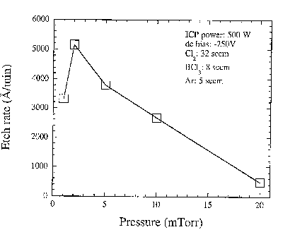
Etch characteristics are often dependent upon plasma parameters including pressure, ion energy and plasma density. As a function of pressure, plasma conditions including the mean free path and the collisional frequency can change resulting in changes in both ion energy and plasma density. GaN etch rates are shown as a function of pressure for an ICP-generated BCl3/Cl2 plasma in Figure 5. Etch rates increased as the pressure was increased from 1 to 2 mTorr and then decreased at higher pressures. The initial increase in etch rate suggested a reactant limited regime at low pressure, however at higher pressures the etch rates decreased due either to lower plasma densities (ions or radical neutrals), redeposition or polymer formation on the substrate surface. At pressures <10 mTorr, GaN etches were anisotropic and smooth, while at pressure >10 mTorr the etch profile was undercut and poorly defined due to a lower mean free path, collisional scattering of the ions and increased lateral etching of the GaN.
GaN etch rates as a function of pressure in an ICP-generated BCl3/Cl2/Ar plasma at 32 sccm Cl2, 8 sccm BCl5, 5 sccm Ar, 500 W IPC source power, dc-bias -150 V and 10°C electrode temperature.
GaN etch rates are plotted as a function of dc bias (which correlates to ion energy) for an ICP-generated BCl3/Cl2 plasma in Figure 6. The GaN etch rates increased monotonically as the dc bias or ion energy increased. Etch rates increased due to improved sputter desorption of etch products from the surface as well as more efficient breaking of the Ga-N bonds. Etch rates have also been observed to decrease under high ion bombardment energies due to sputter desorption of reactive species from the surface before the reactions occur. This is often referred to as an adsorption limited etch regime. In Figure 7, SEM micrographs are shown for (a) −50, (b) −150 and (c) −300 V dc bias. The etch profile became more anisotropic as the dc bias increased from -50 to -150 V dc bias due to the perpendicular path of the ions relative to the substrate surface which maintained straight wall profiles. However, as the dc bias was increased to −300 V, a tiered etch profile with vertical striations in the sidewall was observed due to erosion of the resist mask edge. The GaN may become rougher at these conditions due to mask redeposition and preferential loss of N2.
GaN etch rates as a function of dc bias in an ICP-generated BCl3/Cl2/Ar plasma at 32 sccm Cl2, 8 sccm BCl3, 5 sccm Ar, 500 W ICP source power, 2 mTorr pressure and 10°C electrode temperature.

. SEM micrographs for GaN etched at (a) -50, (b) -150 and (c) −300 V dc bias. ICP etch conditions were 32 sccm Cl2, 8 sccm BCl3, 5 sccm Ar, 500 W ICP source power, 2 mTorr pressure and 10°C electrode temperature.

In Figure 8, GaN etch rates are shown as a function of ICP-source power while the dc bias was held constant at -250 V. GaN etch rates increased as the ICP source power increased due to higher concentrations of reactive species which increases the chemical component of the etch mechanism and/or higher ion flux which increases the bond breaking and sputter desorption efficiency of the etch. Etch rates have also been observed to stabilize or decrease under high plasma flux conditions due either to saturation of reactive species at the surface or sputter desorption of reactive species from the surface before the reactions occur. The etch profile was anisotropic and smooth up to 1000 W ICP power where the feature dimensions were lost and sidewall morphology was rough due to erosion of the mask edge under high plasma flux conditions. In addition to etch rates, etch selectivity or the ability to etch one film at higher rates than another can be very important in device fabrication. For example, optimization of etch selectivity is critical to control threshold voltage uniformity for high electron mobility transistors (HEMTs), to accurately stop on either the emitter or collector regions for metal contacts for heterojunction bipolar transistors (HBTs), and for low resistivity n-ohmic contacts on InN layers. Several studies have recently reported etch selectivity for the group-III nitrides Reference Adesida, Edgar, Strite, Akasaki, Amano and Wetzel[6] Reference Shul, McClellan, Pearton, Abernathy, Constantine and Barratt[7] Reference Shul and Pearton[8]. For example, Figure 9 shows GaN, InN and AlN etch rates and etch selectivities as a function of cathode rf power in an ICP-generated Cl2/Ar plasma. Etch rates for all three films increased with increasing cathode rf power or dc bias due to improved breaking of the III-N bonds and more efficient sputter desorption of the etch products. Increasing InN etch rates were especially significant since InCl3, the primary In etch product in a Cl-based plasma, has a relatively low volatility. However, under high dc-bias conditions, desorption of the InCl3 etch products occurred prior to coverage of the etch surface. The GaN:InN and GaN:AlN etch selectivities were <8:1 and decreased as the cathode rf power or ion energy increased. Smith and co-workers reported similar results in a Cl2-Ar ICP plasma where GaN:AlN and GaN:AlGaN selectivities decreased as dc bias increased. At −20 V dc bias, etch selectivities of ~39:1 were reported for GaN:AlN and ~10:1 for GaN:AlGaN. Temperature dependent etching of the group-III nitrides have been reported in ECR and ICP etch systems Reference Pearton, Shul, Pankove and Moustakas[5]. Etch rates are often influenced by the substrate temperature which can effect the desorption rate of etch produce, the gas-surface reaction kinetics and the surface mobility of reactants. Substrate temperature can be controlled and maintained during the etch process by a variety of clamping and backside heating or cooling procedures. GaN and InN etch rates are shown in Figure 10 as a function of temperature in Cl2/H2/Ar ICP plasma. GaN etch rates were much faster than InN due to higher volatility of the GaCl3 etch products as compared to InCl3 and showed little dependence on temperature. However, the InN etch rates showed a considerable temperature dependence increasing at 150°C due to higher volatilities of the InCl3etch products at higher substrate temperatures.
GaN etch rates as a function of ICP source power in an ICP-generated BCl3/Cl2/Ar plasma at 32 sccm Cl2, 8 sccm BCl3, 5 sccm Ar, -250 V dc bias, 2 mTorr pressure and 10°C electrode temperature.

GaN, InN and AlN (a) etch rates and (b) GaN:AlN and GaN:InN etch selectivities as a function of dc bias in a Cl2/Ar ICP plasma. Plasma conditions were: 25 sccm Cl2, 5 sccm Ar, 2 mTorr chamber pressure, 500 W ICP-source power and 25°C cathode temperature.

GaN and InN etch rates as a function of temperature for an ICP-generated Cl2/H2/Ar plasmas. ICP etch conditions were 22.5 sccm Cl2, 2.5 sccm H2, 5 sccm Ar, 500 W ICP source power, -250 V dc bias and 2 mTorr pressure.

GaN etch rates in an ICP and ECR Cl2H2/Ar plasma as a function of %H2.

GaN etch rates in an ICP and ECR BCl3/H2/Ar plasma as a function of

Several different plasma chemistries have been used to etch the group-III nitrides. As established above, etch rates and profiles can be strongly affected by the volatility of the etch products formed. Table I shows the boiling points of possible etch products for the group-III nitrides exposed to halogen- and hydrocarbon-based plasmas. For halogen-based plasmas, etch rates are often limited by the volatility of the group-III halogen etch product. For Ga- and Al-containing films, chlorine-based plasmas typically yield fast rates with anisotropic, smooth etch profiles. CH4/H2-based plasma chemistries have also yielded smooth, anisotropic profiles for Ga-containing films, however at much slower rates. Based only on a comparison of etch product volatility, slower etch rates in CH4-based plasmas is unexpected since the (CH3)3Ga etch product has a much lower boiling point than GaCl3. This observation demonstrates the complexity of the etch process where redeposition, polymer formation, and gas-phase kinetics can influence the results. As shown above, etch rates for In-containing films obtained in room temperature chlorine-based plasmas tend to be slow with rough surface morphology and overcut profiles due to the low volatility of the InCl3 and preferential loss of the group-V etch products. However, at elevated temperatures (>130°C), the InCl3 volatility increases and the etch rates and surface morphology improve. Significantly better room temperature etch results are obtained in CH4/H2-based plasmas due to the formation of more volatile (CH3)3In etch products. Another example of plasma chemistry dependent etching of GaN is shown in Figure 13 for Cl2/N2/Ar and BCl3/N2/Ar ICP-generated plasmas. In the Cl2-based plasma, GaN etch rates decreased as the % N2 increased, presumable due to a reduction in reactive Cl. In the BCl-based plasma GaN etch rates increased up to 40% N2 and then decreased at higher N2 concentration. This observation has also been reported for ECR and ICP etching of GaAs, GaP and In-containing films Reference Shul and Pearton[8]. Ren and co-workers first observed maximum etch rates for In-containing films (InGaN and InGaP) in an ECR discharge at a gas ratio of 75/25 for BCl3/N2 Reference Ren, Pearton, Shul and Han[10]. Using optical emission spectroscopy (OES), Ren reported maximum emission intensity for atomic and molecular Cl at 75% BCl3 as well as a decrease in the BCl3 intensity and the appearance of a BN emission line. The authors speculated that N2 enhanced the dissociation of BCl3 resulting in higher concentrations of reactive Cl and Cl ions and thus higher etch rates.
Boiling points for possible etch products of Group-III nitride films etched in halogen- or CH4/H2-based plasmas.

GaN etch rates as a function of %N2 for ICP-generated Cl2- and BCl3-based plasmas.

Additionally, the observation of BN emission suggested that less B was available to recombine with reactive Cl. This explanation may also be applied to the peak GaN etch rates observed at 40% N2 in the ICP BCl3/N2/Ar plasmas. However, OES of the BCl3/N2/Ar ICP discharge did not reveal higher concentrations of reactive Cl nor a BN peak emission. In Figure 14, OES spectra are shown for (a) 100% BCl3 (b) 75% BCl3-25% N2, (c) BCl3-75% N2 and (d) 100% N2 ICP plasmas. As N2 was added to the BCl3 plasma, the BCl3 emission (2710 Å) and Cl emission (5443 and 5560 Å) decreased while the BN emission (3856 Å) was not obvious. BCl3/Cl2 plasmas have shown encouraging results in the etching of GaN films. The addition of BCl3 to a Cl2 plasma can improve sputter desorption due to higher mass ions and reduce surface oxidation by gettering H2O from the chamber. In Figure 15, GaN etch rates are shown as a function of % Cl2 in a BCl3/Cl2/Ar ICP plasma. As the % Cl2 increased, GaN etch rates increased up to 80% due to higher concentrations of reactive Cl. OES showed the Cl emission intensity increased and the BCl emission intensity decreased as the % Cl2 increased.
Optical emission spectra (%OES) for an ICP-generated BCl3/N2 plasma as a function of BCl3 percentage.

GaN etch rates in an ICP BCl3/Cl2 plasmas as a function of Cl2.

Slower GaN etch rates in a pure Cl2 plasma were attributed to less efficient sputter desorption of etch products in the absence of BCl3. The fastest GaN etch rates were observed at 10% BCl3 where the ion current density and Cl radical density were the greatest as measured by OES and a Langmuir probe. In general, GaN:AlN and GaN:InN etch selectivities are <10:1 as a function of plasma chemistry for Cl2- or BCl3-based plasmas. GaN:AlN and GaN:InN etch selectivities were higher for Cl2-based ICP plasmas as compared to BCl3-based ICP plasma due to higher concentration of reactive Cl produced in the Cl2-based plasmas thus resulting in faster GaN etch rates. Alternatively, InN and AlN etch rates showed much less dependence on plasma chemistry and were fairly comparable in Cl2- and BCl3-based plasmas. An example of etch selectivity dependence on plasma chemistry is shown in Figure 16. GaN, AlN and InN etch rates and etch selectivities are plotted as a function of % SF6 for an ICP Cl2/SF6/Ar plasma. GaN and InN etch rates decreased as SF6 was added to the plasma due to the consumption of Cl by S and therefore lower concentrations of reactive Cl. The AlN etch rates increased with the addition of SF6 and reached a maximum at 20% SF6. As SF6 was added to the Cl2 plasma, slower AlN etch rates were expected due to the formation of low volatility AlF3 etch products. However, due to the high ion flux in the ICP, the sputter desorption of the AlF3 may occur prior to passivation of the surface. Therefore, the GaN:AlN selectivity decreased rapidly from ~6:1 to <1:1 with the addition of SF6. The GaN:InN selectivity reached a maximum of 4:1 at 20% SF6.
GaN, InN and AlN (a) etch rates and (b) GaN:AlN and GaN:InN etch selectivities

The simple Cl2/Ar chemistry works very well for most device fabrication processes, providing controllable etch rates. Even at biases <90 V, the GaN etch rate is still typically ~1000Å·min−1.
3.2 I2 and Br2 Based
Other halogen-containing plasmas including ICl/Ar, IBr/Ar, BBr3/Ar and BI3/Ar have been used to etch GaN with promising results Reference Pearton, Shul, Pankove and Moustakas[5] Reference Adesida, Edgar, Strite, Akasaki, Amano and Wetzel[6] Reference Shul and Pearton[8]. Vartuli and co-workers reported GaN, InN, AlN, InN, InAlN and InGaN etch rates and selectivities in ECR ICl/Ar and IBr/Ar plasmas Reference Pearton, Shul, Pankove and Moustakas[5]. In general, etch rates increased for all films as a function of dc bias due to improved III-N bond breaking and sputter desorption of etch products from the surface. GaN etch rates >1.3 μm/min were obtained in the ICl/Ar plasma at a rf power of 250 W (bias of −200 V) while GaN etch rates were typically <4000 Å/min in IBr/Ar. Cho et.al. reported GaN etch rates typically <2000 Å/min in ICP-generated BI3/Ar and BBR3/Ar plasmas Reference Pearton, Shul, Pankove and Moustakas[5]. ICl/Ar and IBr/Ar ECR plasmas yielded GaN:InN, GaN:AlN, GaN:InGaN and GaN:InAlN selectivities <6:1, however, etch selectivities >100:1 were obtained for InN:GaN and InN:AlN in BI3/ar plasmas. Fast etch rates obtained for InN were attributed to the high volatility of the InI3 etch products as compared to the GaI3 and AlI3 etch products which can form passivation layers on the surface. Maximum selectivities of ~100:1 for InN:AlN and ~7.5 for InN:GaN were reported in the BBr3/Ar plasma. InIx products have higher volatility than corresponding InGlx species, making iodine an attractive enchant for InGaN alloys. The inter-halogen compounds are weakly bonded, and therefore should easily break apart under plasma excitation to form reactive iodine, bromine and chlorine.
Figure 17 shows etch rates for the binary nitrides and selectivities for InN over both GaN and AlN as a function of the boron halide percentage by flow in the gas load. The dc chuck self-bias decreases as the BI3 content increases, suggesting that the ion density in the plasma is increasing. The InN etch rate is proportional to the BI3 content, indicating the presence of a strong chemical component in its etching. In comparison, AlN and GaN show very low rates until ~50% BI3 (~500 Å/min−1 for AlN and ~1700 Å/min−1 for GaN). An increase in the BI3 content in the discharges actually produces a falloff in the etch rate for both AlN and GaN. We expect there are several possible mechanisms by which to explain these data. First, the decrease in chuck self-bias and hence ion energy under these conditions may more than compensate for the higher active iodine neutral flux. Second, the formation of the less volatile GaIx and AlIx etch products may create a selvege layer which suppresses the etch rate. This mechanism occurs in the Cl2 reactive ion etching of InP. In this system, etching does not occur unless elevated sample temperatures or higher dc biases are used to facilitate removal of the InCl3 etch product. In InN etch selectivity to both materials initially increases but also goes through a minimum. Note, however, that selectivities of >100 can be achieved for both InN/AlN and InN/GaN.
Nitride etch rates (top) and etch selectivities for InN/AlN and InN/GaN (bottom in BI3/Ar or BBr3/Ar discharges (750 W source power, 5 mTorr) as a function of the boron halide content.

Data for BBr3/Ar discharges are also shown in Figure 17 for fixed source power (750 W) and rf chuck power (350 W). Higher rf powers were required to initiate etching with BBr3 compared to BI3 and the dc self-bias increased with the BBr3 content. The etch rate of InN is again a strong function of the boron halide content, while GaN shows significant rates (~1800 Å/min−1) only for pure BBr3 discharges, AlN shows very low etch rates over the whole range of conditions investigated. Maximum selectivities of ~100:1 for InN/AlN and ~7.5:1 for InN/GaN are obtained.
Based on the results in Figure 17, we chose fixed plasma compositions, and varied the ion energy and flux through control of the source and chuck powers. Figure 18 shows that source power had a significant effect only on the InN etch rate for both 4BI3/6Ar and 4BBr3/6Ar discharges at fixed rf power (150 W). The etch rate of InN continues to increase with source power, which controls the ion flux and dissociation of the discharge, whereas the GaN and AlN rates are low for both plasma chemistries. The InN etch rates are approximately a factor of 2 faster in BI3/Ar than in BBr3/Ar even for lower rf chuck powers. This is expected from taking into consideration the relative stabilities of the respective In etch products (the InI3 melting point is 210°C; InBr3 sublimes at <600°C). The resultant selectivities are shown at the bottom of Figure 18; once again a value of ~100:1 for InN over GaN is achieved with BI3, whereas BBr3 produced somewhat lower values.
Nitride etch rates (top) and etch selectivities for InN/AlN and InN/GaN (bottom) in BI3/Ar or BBr3/Ar discharges as a function of source power.

The dependence of the etch rate and InN/AlN and InN/GaN selectivities on rf chuck power for both plasma chemistries at fixed source power (750 W) is shown in Figure 19. While the GaN and AlN etch rates (top left) increase only at the highest chuck powers investigated for 4BI3/6Ar discharges, the InN etch rate increases rapidly to 250 W. This is consistent with a strong ion-assisted component for the latter under these conditions. The subsequent decrease in the etch rate at higher power produces corresponding maxima (≥100) in etch selectivity for chuck powers in the range of 150-250 W. This type of behavior is quite common to high density plasma etching of III-V materials, where the etching is predominantly ion-assisted desorption of somewhat volatile products, with insignificant rates under ion-free conditions. In this scenario, at very high ion energies, the active etching species (iodine neutral in this case) can be removed by sputtering before they have a chance to complete the reaction with substrate atoms. Similar data for BBr3/Ar mixtures are also shown in Figure 19. For this chemistry the InN etch rate saturates and we did not observe any reduction in etch rate, although this might be expected to occur if higher powers could be applied (over power supply is limited to 450 W). GaN does show an etch rate maximum at ~350 W, producing a minimum in the resultant InN/GaN selectivity. The etch selectivity of InN over the other two nitrides for BI3/Ar is again much higher than for BBr3/Ar.
Nitride etch rates (top) and etch selectivities for InN/AlN and InN/GaN (bottom) in BI3/Ar or BBr3/Ar discharges as a function of rf chuck power.

The effect of plasma composition on etch rates and selectivities if GaN, AlN and InN in ICl/Ar and IBr/Ar discharges at 750 W source power, 250 W rf chuck power and 5 mTorr is shown in Figure 20. The etch rates of InN and AlN are relatively independent of the plasma composition for both chemistries over a broad composition range, indicating the etch mechanism is dominated by physical sputtering. The dc bias voltage increased with increasing interhalogen concentrations. The decrease in ion flux also implies an increase in the concentrations of neutral species such as Cl, Br and I. The etch rate of GaN steadily increased with increasing ICl concentration. By contrast the etch rate of GaN saturated beyond 66.7% IBr. These results indicate that etching of GaN in both chemistries can be attributed more to chemical etching by increased concentrations of reactive neutrals than to ion-assisted sputtering. The effect of plasma composition showed an overall trend of decrease in selectivities for InN over both AlN and GaN as the concentration of ICl and IBr increased.
Nitride etch rates (top) and etch selectivities for InN/AlN and InN/GaN (bottom) in ICl/Ar or IBr/Ar discharges (750 W source power, 250 W rf chuck power, 5 mTorr) as a function of interhalogen content.

3.3 CH4/H2/Ar
Pearton and co-workers were the first to etch group-III nitride films in an ECR-generated CH4/H2/Ar plasma Reference Pearton, Shul, Pankove and Moustakas[5]. Etch rates for GaN, InN and AlN were <400 Å/min at ~-250 V dc bias. Vartuli et.al. reported ICP GaN, InN and AlN etch rates approaching 2500 Å/min in CH4/H2Ar and CH4/H2/N2 plasmas Reference Pearton, Shul, Pankove and Moustakas[5]. Etch rates increased with increasing dc bias or ion flux and were higher in CH4/H2/Ar plasmas. Anisotropy and surface morphology were good over a wide range of conditions. As compared to Cl-based plasmas, etch rates were consistently slower which may make the CH4/H2-based processes applicable for devices where etch depths are relatively shallow and etch control is extremely important.
Vartuli and co-workers compared etch selectivities in CH4/H2/Ar and Cl2/Ar plasmas in both RIE- and ECR-generated plasmas Reference Pearton, Shul, Pankove and Moustakas[5]. For CH4/H2/Ar plasmas, InN:GaN and InGaN:GaN etch selectivities ranged from 1:1 to 6:1 whereas etch selectivities of 1:1 or favoring GaN over the In-containing films was reported for Cl2/Ar plasmas.
4. Etch Profile And Etched Surface Morphology
Sidewall morphology is especially critical in the formation of laser mesas for ridge waveguide emitters or for buried planar devices. The vertical striations observed in the GaN sidewall in Figure 21(a) were due to striations in the photoresist mask which were transferred into the GaN feature during the etch. The sidewall morphology and in particular the vertical striations were improved in an ICP Cl2/BCl3 plasma at −150 V dc bias. The etch conditions were at 2 mTorr chamber pressure, 500 W ICP power, 32 sccm Cl2, 8 sccm BCl3, 5 sccm Ar, 25°C temperature, and a dc bias of -150±10 V. Ren et.al. have demonstrated improved GaN sidewall morphology etched in an ECR using a SiO2 mask. Vertical striations in the SiO2 mask were reduced by optimizing the lithography process used to pattern the SiO2. The SiO2 was then patterned in a SF6/Ar plasma in which a low temperature dielectric overcoat was used to protect the resist sidewall during the etch.
SEM micrographs of (a) GaN, (b) AlN and (c) InN etched in Cl2-based ICP plasmas.

In several studies atomic force microscopy (AFM) has been used to quantify the etched surface morphology as root-mean-square (rms) roughness. Rough etch morphology often indicates a nonstoichiometric surface due to preferential removal of either the group-III or group-V species.
A summary of etch rate results for the nitrides with different chemistries and different techniques is shown in Table II.
Summary of etch rate results for GaN, AlN and InN with different plasma chemistries in different techniques.

5. Plasma-Induced Damage
Plasma-induced damage often degrades the electrical and optical properties of compound semiconductor devices. Since GaN is more chemically inert than GaAs and has higher bonding energies, more aggressive etch conditions (higher ion energies and plasma flux) may be used with potentially less damage to the material. Limited data have been reported for plasma-induced damage of the group-III nitrides Reference Pearton, Shul, Pankove and Moustakas[5] Reference Eddy and Molnar[11]. Pearton and co-workers reported increased plasma-induced damage as a function of ion flux and ion energy for InN, InGaN and InAlN in an ECR Reference Pearton, Shul, Pankove and Moustakas[5]. The authors also reported: (a) more damage in InN films as compared to InGaN; (b) more damage in lower doped materials and (c) more damage under high ion energy conditions due to formation of deep acceptor states which reduce the carrier mobility and increased resistivity. Postetch annealing processes removed the damage in the InGaN while the InN damage was not entirely removed.
Ren and co-workers measured electrical characteristics for InAlN and GaN FET structures to study plasma-induced damage for ECR BCl3, BCl3/N2 and CH4/H2 plasmas Reference Ren, Pearton, Shul and Han[10]. They reported: (a) doping passivation in the channel layer in the presence of hydrogen; (b) high ion bombardment energies can create deep acceptor states that compensate the material and (c) preferential loss of N can produce rectifying gate characteristics. Ping and co-workers studied Schottky diodes for Ar and SiCl4 RIE plasmas Reference Adesida, Edgar, Strite, Akasaki, Amano and Wetzel[6]. More damage was observed in pure Ar plasmas and under high dc-bias conditions. Plasma-induced damage of GaN was also evaluated in ICP and ECR Ar plasma using photoluminescence (PL) measurements as a function of cathode rf power and source power Reference Shul, Briggs, Han, Pearton, Lee, Vartuli, Killeen and Ludowise[12]. The peak PL intensity decreased with increasing ion energy independent of etch technique. As a function of source power or plasma density the results were less consistent. The PL intensity showed virtually no change at low ICP source power and then decreased as the plasma density increased. In the ECR plasma, the PL intensity increased by ~115% at low ECR source power and improved at higher ECR source powers but at a lower rate. The effect of postetch annealing in Ar varied depending on initial film conditions, however, annealing at temperatures above 440°C resulted in a reduction in the PL intensity.
Surface stoichiometry can also be used to evaluate plasma-induced damage. Nonstoichiometric surfaces can be created by preferential loss of one of the lattice constituents. This may be attributed to higher volatility of the respective etch products, leading to enrichment of the less volatile species, or preferential sputtering of the lighter element. Auger electron spectroscopy (AES) can be used to measure surface stoichiometry. Figure 22 shows characteristic Auger spectra for (a) as-grown GaN samples and samples exposed to an ECR plasma t 850 W applied microwave power and cathode rf powers of (b) 65 and (c) 275 W. For the as-grown sample, the Auger spectrum showed a Ga:N ratio of 1.5 with normal amounts of adventitious carbon and native oxide on the GaN surface. Following plasma exposure, the Ga:N ratio increased as the cathode rf power increased with some residual atomic Cl from the plasma. Under high ion energy conditions, preferential removal of the lighter N atoms as observed resulting in Ga-rich surfaces.
AES surface scans of GaN (a) before exposure to the plasma, (b) at 65 W (-120 V bias) and (c) 275 W rf-cathode power (−325 V bias), 1 mTorr, 170°C, and 850 W microwave power in an ECR-generated Cl2/H2 discharge.

5.1 n-GaN
The etching requirements for electronic devices are more demanding than those for photonic devices, at least from the electrical quality viewpoint. One of the most sensitive tests of near-surface electrical properties is the quality of rectifying contacts deposited on the etched surface. There has been relatively little work in this area to date. Ren et.al. Reference Ren, Pearton, Shul and Han[10]. found that rectifying contacts on electron cyclotron resonance plasma etched GaN and InAlN surfaces were very leaky, though some improvement could be obtained by postetch annealing at 400°C. Ping et.al. Reference Adesida, Edgar, Strite, Akasaki, Amano and Wetzel[6]. found that reactively ion etched n-GaN surfaces had poor Schottky contact properties, but that plasma chemistries with a chemical component (e.g. Cl2-based mixtures) produced less degradation than purely physical etching.
The layer structure and contact metals are shown schematically in Figure 23. The GaN was grown by rf plasma-assisted molecular beam epitaxy on c-plane Al2O3 substrates. The Ti/Au ohmic contracts were patterned by lift-off and annealed at 750°C, producing contact resistances in the 10−5 Ωcm−2 range. Samples were exposed to either pure N2 or H2 discharges in a Plasma Therm 790 ICP system at a fixed pressure of 5 mTorr. The gases were injected into the ICP source at a flow rate of 15 standard cubic centimeters per minute (sccm). The experimentally varied parameters were source power (300-1000 W) and rf chuck power (40-250 W), which control ion flux and ion energy, respectively. In some cases the samples were either annealed in N2 for 30 s at 300-850°C, or photoelectrochemically etched in 0.2 M KOH solutions at 25°C after plasma exposure. The Pt/Au Schottky metallization was then deposited through a stencil mass by e-beam evaporation. Current-voltage characteristics were recorded on a HP4145A parameter analyzer, and we defined the reverse breakdown voltage (VB) as the voltage at which the leakage current was 10−3 A. We found in all cases that plasma exposure caused significant increases in forward and reverse current, with ideality factors increasing from typical values of 1.4-1.7 on control samples to >2. For this reason we were unable to extract meaningful values of either ideality factor or barrier height. Figure 24 shows a series of I-V characteristics from the GaN diodes fabricated on samples exposed to either H2 or N2 discharges at different source powers. It is clear that N2 plasma exposure creates more degradation of the diode characteristics than does H2 exposure. This implicates the ion mass (28N2 +, 2H2 + for the main positive ion species) as being more important in influencing the electrical properties of the GaN surface than a chemical effect, since H2 would be likely to preferentially remove nitrogen from the GaN as NH3.
Schematic of GaN Schottky diode structure.

I-V characteristics from GaN diodes before and after H2 (top) or N2 (bottom) plasma exposure (150 W rf chuck power, 5 mTorr) at different ICP source powers.

The variations of VB of the diodes with the source power during plasma exposure are shown in Figure 25. For any exposure to the N2 discharges VB is severely reduced. By contrast there is less degradation with the H2 plasma to the lower average ion energy at those conditions, as shown at the bottom of Figure 25. The average ion energy is approximately equal to the sum of dc self-bias and plasma potential, with the later being in the range −22 to −28 V as determined by Langmuir probe measurements. Ion induced damage in GaN displays n-type conductivity, and in addition the heavy N2 + ions are also more effective in preferential sputtering of the N relative to Ga, compared to the H2 + ions of similar energy.
Variation of VB in GaN diodes (top) and dc chuck self-bias (bottom) as a function of ICP source power in H2 or N2 plasmas (150 W rf chuck power, 5 mTorr).

Similar conclusions can be drawn from the data on the effect of increasing rf chuck power. There were once again very severe decreases in breakdown voltage and increase in leakage current. The VB values fall by more than a factor of two even for very low self-biases, and emphasize how sensitive the GaN surface is to degradation by energetic ion bombardment. The degradation saturates beyond ~100 W chuck power, corresponding to ion energies of ~175 eV. We assume that once the immediate surface becomes sufficiently damaged, the contact properties basically cannot be made any worse and the issue is then whether the damage depth increases with the different plasma parameters. Since ion energy appears to be a critical factor in creating the near-surface damage, we would expect damage depth to increase with ion energy in a nonetching process. In the case of simultaneous etching and damage creation (e.g. in Cl2/Ar etch processing), higher etch rates would lead to lower amounts of residual damage because the disordered region would be partially removed.
The damage depth was established by photoelectrochemically wet etching different amounts of the plasma-exposed GaN surfaces, and then depositing the Pt/Au metal. Figure 26 (top) show the effect on the I-V characteristics of this removal of different depth of GaN. There is a gradual restoration of the reverse breakdown voltage, as shown at the bottom of the figure. Note that the forward part of the characteristics worsens for removal of 260 Å of GaN, and shows signs of high series resistance. This would be consistent with the presence of a highly resistive region underneath the conducting near-surface layer, created by point defect diffusion from the surface. A similar model applies to ion-damaged InP, i.e. a nonstoichiometric near-surface region (deficient in P in that case), followed by a transition to a stoichiometric but point defect-compensated region, and finally to unperturbed InP.
I-V characteristics from N2 plasma exposed GaN diodes before and after wet etch removal of different amounts of GaN prior to deposition of the Schottky contact (top) and variation of VB as a function of the amount of material removed (bottom).

The fact that plasma exposure severely degraded the surface was clear from the atomic force microscopy (AFM) data. Exposure to the 500 W source power, 150 W rf chuck power (dc self-bias – 221 V), 5 mTorr N2 discharge increased the root-mean-square (rms) surface roughness form 0.8 to 4.2 nm. Subsequent photoelectrochemical etching restored the initial morphology. However, we observed the onset of increasingly rough surfaces for deeper etch depths Reference Nakamura and Fasol[4], reducing a relatively inaccurate measure of how much of the surface had to be removed in order to restore the diode breakdown voltage to its original value. We were able to estimate this depth as ~600 ± 150 Å for the N2 plasma conditions mentioned above. Another method for trying to restore the electrical properties of the plasma-exposed surface is annealing. I-V data from annealed samples are shown in Figure 27. At the top are characteristics from samples, which were plasma exposed (N2, 500 W source power, 150 W rf chuck power, 5 mTorr), then annealed and the contact deposited. These samples show that increasing annealing temperature up to 750°C brings a substantial improvement in VB (Figure 27, bottom). However for annealing at 850°C the diode began to degrade and this is consistent with the temperature at which N2 begins to be lost from the surface. In the case where the samples were exposed to the N2 plasma, and then the Pt/Au contact was deposited prior to annealing, the I-V characteristics show continued worsening upon annealing (Figure 27, center). In this case, the Pt/Au contact is stable to 700°C on unetched samples. The poorer stability in etched samples could be related to the surface damage enhancing interfacial reaction between the Pt and GaN.
I-V characteristics from GaN diodes before and after N2 plasma exposure (500 W source power, 150 W rf chuck power, 5 mTorr) and subsequent annealing either prior (top) or subsequent (center) to the deposition of the Schottky metallization. The variation of VB in the samples annealed prior to metal deposition is shown at the bottom of the figure.

The main findings of this study can be summarized as follows:
There is a severe degradation in the electrical quality of GaN surfaces after ICP H2 or N2 discharge exposure. Under all conditions there is a strong reduction of VB in diode structures to the point at which the Schottky contacts show almost ohmic-like behavior. These observations are consistent with the creation of a conducting n-type surface layer resulting from energetic ion bombardment. Heavier ions (N2 +) create more damage than lighter ions (H2 +) in this situation, where damage is accumulating without any concurrent etching of the surface.
The depth of the damage is approximately 600 Å, as judged by the return of the diode characteristics to their control values.
Annealing at 750°C is also effective in helping remove the effects of plasma exposure. Higher temperatures lead to degradation in GaN diode properties for uncapped anneals.
5.2 p-GaN
The layer structure consisted of 1μm of undoped GaN (n~5×1016 cm-3) grown on a c-plane Al2O3 substrate, followed by 0.3μm of Mg doped (p~1017 cm-3) GaN. The samples were grown by rf plasma-assisted Molecular Beam Epitaxy. Ohmic contacts were formed with Ni/Au deposited by e-beam evaporation, followed by lift-off and annealing at 750−oC. The GaN surface was then exposed for 1 min to ICP H2 or Ar plasmas in a Plasma-Therm 790 System. The 2MHz ICP source power was varied from 300-1400 W, while the 13.56 MHz rf chuck power was varied from 20-250 W. The former parameter controls ion flux incident on the sample, while the latter controls the average ion energy. Prior to deposition of 250μm diameter Ti/Pt/Au contacts through a stencil mask, the plasma exposed surfaces were either annealed under N2 in a rapid thermal annealing system, or immersed in boiling NaOH solutions to remove part of the surface. As reported previously it is possible to etch damaged GaN in a self-limiting fashion in hot alkali or acid solutions. The current-voltage (I-V) characteristics of the diodes were recorded on a HP 4145A parameter analyzer. The unetched control diodes have reverse breakdown voltages of ~2.5-4 V depending on the wafer – these values were uniform (±12%) across a particular water.
Figure 28 shows the I-V characteristics from samples exposed to either H2 (top) or Ar (bottom) ICP discharges (150 W rf chuck, 2 mTorr) as a function of source power. In both cases there is an increase in both the reverse breakdown voltage and the forward turn-on voltage, with these parameters increasing monotonically with the source power during plasma exposure.
I-V characteristics from samples exposed to either H2 (top) or Ar (bottom) ICP discharges (150 W rf chuck power) as a function of ICP source power prior to deposition of the Ti/Pt/Au contact.

Figure 29 shows this increase in breakdown voltage as a function of source power, and also the variation of the chuck dc self-bias. As the source power increases, the ion density also increases and the higher plasma conductivity suppresses the developed dc bias. Note that the breakdown voltage of the diodes continues to increase even as this bias (and hence ion energy, which is the sum of this bias and the plasma potential) decreases. These results show that ion flux lays an important role in the change of diode electrical properties. The other key result is that Ar leads to consistently more of an increase in breakdown voltage, indicating that ion mass is important rather than any chemical effect related to removal of N2 or NH3 in the H2 discharges.
Variation of diode breakdown voltage in samples exposed to H2 or Ar ICP discharges (150 W rf chuck power) at different ICP source powers prior to deposition of the Ti/Pt/Au contact. The dc chuck self-bias during plasma exposure is also shown.

The increase in breakdown voltage on the p-GaN is due to a decrease in hole concentration in the near-surface region through the creation of shallow donor states. The key question is whether there is actually conversion to an n-type surface under any of the plasma condition. Figure 30 shows the forward turn-on characteristics of the p-GaN diodes exposed to different source power Ar discharge at low source power (300 W), the turn-on remains close to that of the unexposed control sample. However there is a clear increase in the turn-on voltage at higher source powers, and in fact at ≥ 750 W the characteristics are those of an n-p junction. Under these conditions the concentration of plasma-induced shallow donors exceeds the hole concentration and there is surface conversion. In other words the metal-p GaN diode has become a metal-n GaN-p GaN junction. We always find that plasma exposed GaN surfaces are N2-deficient relative to their unexposed state, and therefore the obvious conclusion is nitrogen vacancies create shallow donor levels. This is consistent with thermal annealing experiments in which N2 loss from the surface produced increased n-type conduction.
Forward turn-on characteristics of diodes exposed to ICP Ar discharges (150 W rf chuck power) at different ICP source powers prior to deposition of the Ti/Pt/Au contact.

An important question is the depth of the plasma-induced damage. We found we were able to etch p-GaN very slowly in boiling NaOH solutions, at rates that depended on the solution molarity (Figure 31) even without any plasma exposure of the material. This enabled us to directly measure the damage depth in plasma exposed samples in two different ways. The first method involved measuring the etch rate as a function of depth from the surface. Defective GaN resulting from plasma, thermal or implant damage can be wet chemically etched at rates much faster than undamaged material because the acid or base solutions are able to attack the broken or strained bonds present. Figure 32 shows the GaN etch rate as a function of depth in samples exposed to a 750 W source power, 150 W rf chuck power Ar discharge. The etch rate is a strong function of the depth from the surface and saturates between ~425-550 Å. Within this depth range the etch rate is returned to the “bulk” value characteristic of undamaged p-GaN.
Wet etching rate of p-GaN in boiling NaOH solutions as a function of solution molarity.

Wet etching rate of Ar plasma exposed (750 W source power, 150 W rf chuck power) GaN as a function of depth into the sample.

I-V characteristics from samples exposed to ICP Ar discharges (750 W source power, 150 W rf chuck power) and subsequently wet etched to different depths prior to deposition of the Ti/Pt/Au contact (top) and breakdown voltage as a function of depth removed (bottom).

The other method of removing plasma-induced damage is annealing. In these experiments we exposed the samples to the same type of plasma (Ar, 750 W source power, 150 W rf chuck power) and then annealed under N2 at different temperatures. Figure 34 (top) shows the I-V characteristics of these different samples, while Figure 34 (bottom) shows the resulting breakdown voltages as a function of annealing temperature. On this wafer, Plasma exposure caused an increase in breakdown voltage from ~2.5 to ~18 V. Subsequent annealing at 400°C initially decreased the breakdown voltage, but higher temperature produced a large increase. At temperatures above 700°C, the diodes characteristics returned toward their initial values and were back to the control values by 900°C. This behavior is similar to that observed in implant-isolated compound semiconductors where ion damage compensates the initial doping in the material, producing higher sheet resistance. In many instances the damage site density is larger than that needed to trap all of the free carriers, and trapped electrons or holes may move by hopping conduction. Annealing at higher temperatures removes some of the damage sites, but there are still enough to trap all the conduction electrons/holes. Under these conditions the hopping conduction is reduced and the sample sheet resistance actually increases. At still higher annealing temperatures, the trap density falls below the conduction electron or hole concentration and the latter are returned to their respective bands. Under these conditions the sample sheet resistance returns to its pre-implanted value. The difference in the plasma exposed samples is that the incident ion energy is a few hundred eV compared to a few hundred keV in implant-isolated material. In the former case the main electrically active defects produced are nitrogen vacancies near the surface, whereas in the latter case there will be vacancy and interstitial complexes produced in far greater numbers to far greater depths. In our previous work on plasma damage in n-GaN we found that annealing at ~750°C almost returned the electrical properties to their initial values. If the same defects are present in both n- and p-type material after plasma exposure, this difference in annealing temperature may be a result of a Fermi level dependence to the annealing mechanism. The main conclusions of this study may be summarized as follow:
I-V characteristics from samples exposed to ICP Ar discharges (750 W source power, 150 W rf chuck power) and subsequently annealed at different temperatures prior to deposition of the Ti/Pt/Au contact (top) and breakdown voltage as a function of annealing temperature (bottom).

The effect of either H2 or Ar plasma exposure on p-GaN surfaces is to decrease the net acceptor concentration through creation of shallow donor levels, most likely NV. At high ion fluxes or ion energies there can be type conversion of the initially p-type surface. The change in electrical properties is more pronounced with Ar than with H2 plasmas under the same conditions.
Two different techniques for measuring the damage depth find it to be in the range 400-500 Å under our conditions. After removing this amount of GaN, both the breakdown voltage and wet chemical etch rates are returned to their initial values.
Post-etch annealing in N2 at 900°C restores the initial breakdown voltage on plasma exposed p-GaN. Annealing at higher temperatures degraded the electrical properties, again most likely due to N2 loss from the surface.
5.1 Schottky Diodes
Contrary to initial expectations, the surface of GaN is relatively sensitive to energetic ion bombardment or thermal degradation encountered during device processing. In particular it can preferentially lose N2, leaving a strong n-type conducting regions. While dry etching has been used extensively for patterning of photonic devices (light-emitting and laser diodes) and opto-electronic devices (UV detectors), there has been little work performed on understanding the electrical effects of ion-induced point defects or non-stoichiometric surfaces resulting from the plasma exposure. Several groups have reported increases in sheet-resistance of GaN exposed to high density plasmas, along with decreases in reverse breakdown voltage (VB) and reductions in Schottky barrier height (ϕB) in diodes formed on n-type GaN. In this latter case, low-bias forward currents were increased up to two orders of magnitude after exposure of the diode to pure Ar discharges. Conversely, while the rectifying contact properties were degraded by plasma exposure, the specific resistance of n-type ohmic contacts was improved. Similarly, in p-type GaN, the effect of Ar or H2 high density plasma exposure was to decrease the net acceptor concentration to depths of ~500 Å. At high ion fluxes or energies, there was type-conversion of the initially p-GaN surface.
Dry etching is needed for a range of GaN electronic devices, including mesa diodes rectifiers, thyristors and heterojunction bipolar transistors for high temperature, high power operation. These applications include control of power flow in utility grids, radar and electronic motor drives. It is critical to understand the depth and thermal stability of dry etch damage in both n- and p-type GaN and its effect on the current-voltage (I-V) characteristics of simple diode structures.
In this section we report on a comparison of the effects of Cl2/Ar and Ar Inductively Coupled Plasma (ICP) exposure on the electrical properties of n- and p-GaN Schottky diodes. In some cases it was found that Cl2/Ar discharges could produce even more damage than pure Ar, due to the slightly higher ion energies involved. The damage saturates after a short exposure to either Cl2/Art or Ar discharges and is significant even for low ion energies. Annealing between 700-800°C restored ≥ 70% of the reverse breakdown voltage on n-GaN, while the damage depth was again established to be ~500 Å in p-GaN.
The GaN layers were grown by rf plasma-assisted Molecular Beam Epitaxy on c-plane Al2O3 substrates. The Ti/Al (for n-type) and Ni/Au (for p-type) ohmic contacts were patterned by lift-off and annealed at 750°C. The samples were exposed to either 10Cl2/5Ar or 15 Ar (where the numbers denote the gas flow rate in standard cubic centimeters per minute) ICP discharges in a Plasma-Therm ICP reactor at a fixed pressure of 3 mTorr. We investigated a range of rf chucks powers (25-250 W) and etch times (4-100 secs), with a fixed source power of 500 W. In some cases, the samples were either annealed in N2 for 30 secs at 500-800°C or wet etching in 0.1M NaOH solutions at ~100°C after plasma exposure. The Schottky metallization (Pt/Au in both cases) was then deposited through a stencil mask (ϕ = 70 or 90μm) by e-beam evaporation. Current-voltage characteristics were recorded on an HP 4145A parameter analyzer, and we defined the reverse breakdown voltage as that at which the leakage current was 10−3A. The forward on-voltage VF was defined as the voltage at which the forward current was 100A·cm−2. In all cases the ideality factors increased from 1.3-1.6 on control samples to >2 after plasma exposure and thus we were unable to extract meaningful values of either barrier height or ideality factor.
Figure 35 shows a series of I-V characteristics from n-type GaN diodes fabricated on samples exposed to either Cl2/Ar (top) or Ar (bottom) discharges at different rf chuck powers. There is a significant reduction in VB under all conditions, with Ar producing less damage at low chuck powers. This is probably related to two factors – the slightly higher chuck bias with Cl2/Ar due to the lower positive ion density in the plasma (Cl is more electronegative than Ar) and the heavier mass of the Cl2 + ions compared to Ar+. This is consistent with our past data on the relative effects of N2 and H2 plasma exposure, in which ion mass was found to be more important in influencing the electrical properties of the GaN surface than any chemical effects.
I-V characteristics from n-GaN samples exposed to ICP Cl2/Ar (top) or Ar (bottom) discharges (500 W source power) as a function of rf chuck power prior to deposition of the rectifying contact.

The variations of VB and VF with the rf chuck power during plasma exposure are shown in Figure 36 (top). At powers ≤ 100, the Cl2/Ar creates more degradation of VB, as discussed above, while at higher powers the damage saturates. The average ion energy is the sum of dc self-bias (shown at the bottom of the figure) and plasma potential (which is about 22-25 eV under these conditions). Thus for ion energies <~150 eV, Ar produces less damage than Cl2/Ar, even though the etch rate with the latter is much higher. This is also reflected in the variation of F with rf chuck power.
Variations of VB and VF (top) and of n-GaN etching rate (bottom) as a function of rf chuck power for n-GaN diodes exposed to ICP Cl2/Ar discharges (500 W source power).

Figure 37 shows a series of I-V characteristics from n-type GaN diodes fabricated on samples exposed to the two different plasmas for different times at fixed rf chuck power (150 W) and source power (500 W). It is clear that the damage accumulates rapidly, with the I-V characteristics becoming linear at longer times. It should be remembered that this is damage accumulating ahead of the etch front. To examine the thermal stability of the etch damage, n-type samples were exposed to Ar or Cl2/Ar discharges at a fixed source power (500 W) and rf chuck power 150 W rf), and then annealed at different temperatures prior to deposition of the rectifying contact. The annealing produces a significant recovery of the electrical properties for samples exposed to either type of plasma. The VB values are shown in Figure 38, as a function of post-plasma exposure annealing temperature. Annealing temperatures between 700-800°C restore > 70% of the original VB value, but clearly annealing alone cannot remove all of the dry etch induced damage. Annealing temperatures above 800°C were found to lead to preferential loss of N2 from the surface, with a concurrent degradation in VB.
I-V characteristics from n-GaN samples exposed to ICP Cl2/Ar (top) or Ar (bottom) discharges (150 W rf chuck power, 500 W source power) as a function of plasma exposure time prior to deposition of the rectifying contact.

Variation of VB in n-GaN diodes exposed to ICP Cl2/Ar or Ar discharges (500 W source power, 100 W rf chuck power) with annealing temperature prior to deposition of the rectifying contact.

I-V characteristics from p-GaN samples exposed to ICP Cl2/Ar (top) or Ar (bottom) discharges (500 W source power, 150 W rf chuck power) and wet etched in boiling NaOH to different depths prior to deposition of the rectifying contact.

Figure 40 shows two methods for determining the depth of the damaged region in p-GaN diodes. At top is a plot of the variation of VF and VB with the depth of material removed by NaOH etching. The values of both parameters are returned to their control values by depths of 500-600 Å. What is clear from this data is that the immediate surface is not where the p-doping concentration is most affected, since the maximum values peak at depths of 300-400 Å. This suggests that NV or other compensating defects created at the surface diffuse rapidly into this region even near room temperature. This is consistent with results in other semiconductors, where damage depths are typically found to be many times deeper than the projected range of incident ions. The bottom part of Figure 40 shows the wet etch depth in plasma damaged p-GaN as a function of etching time. The etch depth saturates at depths of 500-600 Å, consistent with the electrical data. It has previously been shown that the wet etch depth on thermally- or ion-damaged GaN was self-limiting. This is most likely a result of the fact that defective or broken bonds in the material are readily attached by the acid or base, whereas in undamaged GaN the etch rate is negligible.
Variation of VB and VF (top) with depth of p-GaN removed by wet etching prior to deposition of the rectifying contact, and wet etch depth versus etch time in boiling NaOH solutions for plasma damaged p-GaN (bottom).

The main finding of our study may be summarized as follows:
(1) Large changes in VB and VF of n- and p-GaN Schottky diodes were observed after exposure to both Cl2/Ar and Ar ICP discharges. In some cases the electrical properties are more degraded with Cl2/Ar even though this plasma chemistry has a much higher etch rate.
The damage accumulates in the near-surface even for very short exposure times (4 secs). The damage depth was established to be 500-600 Å from both the changes in electrical properties and the depth dependence of wet etch rate.
Annealing in the range 700-800°C partially restores VB in n-GaN diodes, but full recover can only be achieved with an additional wet etch step for removal of the damaged material. The combination of annealing and a wet etch clean-up step looks very promising for GaN device fabrication.
5.1 p-n Junctions
Layer structures were grown by Metal Organic Chemical Vapor Deposition on c-plane Al2O3 substrates at 1040°C. The structure consisted of a low temperature (530°C) GaN buffer, 1.2μm of n (2×1017 cm−3, Si-doped) GaN, 0.5μm of nominally undoped (n~1016 cm−3) GaN and 1.0μm of p (NA ~5×1019 cm−3, Mg-doped) GaN. The p-ohmic metal (Ni/Au) was deposited by e-beam evaporation and lift-off, then alloyed at 750°C. A mesa was then formed by BCl3/Cl2/Ar (8/32/5-sccm) ICP etching to a depth of 1.6μm under different plasma conditions in order to examine the effect of ion energy and ion flux, respectively. The ICP reactor was a load-locked Plasma-Therm SLR 770, which used a 2 MHz, 3-turn coil ICP source. All samples were mounted using a thermally conductive paste on an anodized Al carrier that was clamped to the cathode and cooled with He gas. The ion energy or dc-bias or dc-bias was defined by superimposing a rf-bias (13.56 MHz) on the sample. The n-type ohmic metallization (Ti/Al) was then deposited. Reverse I-V measurements were made on 300μm diameter diodes with a HP 4145B semiconductor parameter analyzer. In this study the reverse leakage current was measured at a bias of -30 V. Etch rates were calculated from bulk GaN samples patterned with AZ-4330 photoresist. The depth of etched features was measured with an Alpha-step stylus profilometer after the photoresist was removed. Etch profile and surface morphology were analyzed with scanning electron microscopy and atomic force microscopy, respectively.
Figure 41 shows the effect of dc chuck bias on the reverse junction leakage current, along with the corresponding GaN etch rates. There is little effect on the current below chuck biases of -250 V. This corresponds to an ion energy of approximately -275 eV, since this energy is the sum of chuck bias and plasma potential (about -25 eV in this tool under these conditions). The reverse current decreases slightly as the dc self-bias is increased from -25 to -50 V. This may result from the sharp increase in etch rate which leads to faster removal of near-surface damage. The reverse current increases rapidly above -275 V ion energy, which is a clear indication of severe damage accumulating on the sidewall. The damage probably takes the form of point defects such as nitrogen vacancies, which increase the n-type conductivity of the surface. The total reverse current density, JR is the sum of three components namely diffusion, generation and surface leakage according to

Reverse leakage current measured at -30 V for GaN p-i-n junctions etched in ICP 32Cl2/8BCl3/5Ar discharges (500 W source power, 2 mTorr), as a function of dc chuck self-bias.

where e is the electronic charge, De,h are the diffusion coefficients of electrons or holes, le,h are the lengths of the n and p regions outside the depletion region in a p-n junction, ND,A are the donor/acceptor concentrations on wither side of the junction, nI is the intrinsic carrier concentration, W the depletion with τg the thermal generation lifetime of carriers and JSL is the surface current component which is bias-dependent. The latter component is most affected by the dry etch process, and dominates the reverse leakage in diodes etched in high ion energies.
GaN sidewall profiles and etch morphologies have been evaluated from previous results as a function of dc-bias. The etch becomes more anisotropic as the dc-bias increased from -50 to -150 V dc-bias due to the perpendicular nature of the ion bombardment energies. However, at -300 V dc-bias a tiered etch profile with vertical striations in the sidewall was observed due to erosion of the mask-edge under high ion bombardment energies. The physical degradation (both profile and morphology) of the etched sidewall at -300 V could help explain higher reverse leakage currents above-250 V dc-bias. Under high bias conditions, more energetic ions scattering from the surface could strike the sidewalls with significant momentum thus increasing the likelihood of increased damage and higher reverse leakage currents. Under low bias conditions, the sidewall profile is less anisotropic implying increased lateral etching of the GaN (undercutting of the mask). Under these conditions the etch process becomes dominated by the chemical component of the etch mechanism, which may account for the slightly higher reverse leakage observed at -25 V dc-bias. Figure 42 shows the effect of ICP source power on the junction reverse leakage current. The plasma flux is proportional to source power. In this experiment the ion energy was held constant at −100 V dc-bias. There is minimal effect on leakage current for source powers ≤ 500 W, with severe degradation of the junction characteristics at higher powers even thought the GaN etch rate continues to increase. This is an important result because it shows that the conditions that produce the highest etch rate are not necessarily those that lead to the least damage. Increased sidewall damage under high plasma flux conditions may be due to increased ion scattering as well as more interactions of reactive neutrals with the sidewall of the mesa. SEM micrographs from bulk GaN samples also show a degradation of sidewall profile under high ICP source power conditions. At an ICP source power of 1000 W, the sidewall has a tiered profile with vertical striations possibly due to erosion of the mask edge. However, sidewall profiles at 250 and 500 W looked reasonably anisotropic and smooth. Reverse leakage currents were relatively insensitive to chemistry effects in a Cl2/BCl3/Ar ICP discharge. The reverse leakage current ranged between ~10 and 40 nA as the %Cl2 changed from 0 to 100. This is not too surprising given that BCl3 ions will be the heaviest ions in the discharge under all these conditions, and we expect ion damage to be dominated at this flue. The reverse leakage currents were measured from a different GaN wafer as compared to other samples used in this study. The surface morphology for the as-grown wafer was significantly higher for this sample and may account for higher reverse leakage currents measured under the standard conditions. Notice the GaN etch rate increased as Cl2 was added to the BCl3/Ar plasma up to 80%. In Cl2/Ar plasma the GaN etch rate decreased due to lower concentrations of reactive Cl neutrals. Etch profiles were relatively anisotropic and smooth except for the Cl2/Ar plasma where the etch was slightly rough.
Reverse leakage current measured at -30 V for GaN p-i-n junctions etched in ICP 32Cl2/8BCl3/5Ar discharges (-100 V dc chuck self-bias, 2 mTorr), as a function of source power.

Two samples were annealed in this study to determine if the defects caused by plasma-induced-damage to the p-n junction could be removed and low reverse leakage currents recovered. The first sample was initially exposed to the following ICP conditions: 32 sccm Cl2, 8 sccm BCl3, 5 sccm Ar, 500 W ICP power, −300 V dc-bias and 2 mTorr pressure. The reverse leakage remained essentially constant up to 600°C where the reverse leakage increased by more than an order of magnitude (see Figure 43). (Note all reverse leakage data were taken at −30 V except for the 600°C data, which was taken at lower voltages due to breakdown at −30 V). A similar trend was observed for the second sample. Although there was much more scatter in the data, which was exposed to the same ICP conditions with the exceptions of 750 W ICP source power and −100 V dc-bias. The inability to remove damage from these samples may be due to anneal temperatures which were not high enough. Improved breakdown voltages for dry etched n- and p-GaN Schottky diodes occur after annealing in the range of 400 to 700°C, however anneal temperatures >800°C were needed to produce near-complete recovery in breakdown voltage.
Reverse leakage current measured at −30 V for GaN p-i-n junctions etched in ICP 32Cl2/8BCl3/5Ar discharges (-300 V dc chuck self-bias, 500 W ICP source power, 2 mTorr), as a function of anneal temperature.

In summary there are high-density plasma etching conditions for GaN where there is minimal degradation in the reverse leakage current of p-i-n mesa diodes. Both ion energy and ion flux are important in determining the magnitude of this current, and a high etch rate is not necessarily the best choice for minimizing dry etch damage.
6. Device Processing
6.1 Microdisk Lasers
A novel laser structure is the microdisk geometry, which does not require facet formation. These lasers should in principle have low thresholds because of their small active volume. While microcylinder geometries are possible, superior performance is expected when the active disk region sits only on a thin support post or pedestal. To fabricate this latter geometry, it is necessary to have a selective wet etch for the material under the active layer. A microcylinder is initially formed by anisotropic dry etching. We have employed ECR or ICP Cl2/Ar discharges to produce the initial vertical etch. The undercut is then produced by use of KOH solutions at ~80°C to selectively etch the AlN buffer layer on which the InGaN/GaN quantum well is grown. SEM micrographs of two different lasers are shown in Figure 44. In both cases we used an upper cladding layer of AlGaN, which was etched somewhat slower than the pure AlN bottom cladding layer.
SEM micrographs of GaN/InGaN/AlN microdisk laser structures.

6.2 Ridge Waveguide Lasers
The achievement of continuous wave GaN-InGaN laser diodes has tremendous technological significance. For commercially acceptable laser lifetimes (typically ≥ 10,000 h), there is immediate application in the compact disk data storage market. The recording and reading of data on these disks are currently performed with near-infrared (~780 nm) laser diodes. The switch to the much shorter wavelength (~400 nm) GaN-based laser diodes will allow higher recording densities [by ~(780/400)2 or almost a factor of 4]. There is also a large potential market in projection displays, where laser diodes with the three primary colors (red, green and clue) would replace the existing liquid crystal modulation system. The laser-based system would have advantages in terms of greater design simplicity, lower cost and broader color coverage. The key development is the need to develop reliable green InGaN laser diodes. The high output power of GaN-based lasers and fast off/on times should also have advantages for improved printer technology, with higher resolution than existing systems based on infrared lasers. In underwater military systems, GaN lasers may have application for covert communications because of a transmission passband in water between 450 and 550 nm.
While a number of groups have now reported room-temperature lasers in the InGaN/GaN/AlGaN heterostructure system under pulsed and cw operation Reference Morkoc[3] Reference Nakamura and Fasol[4], the field has been completely dominated by Nakamura et.al. Reference Nakamura and Fasol[4]. The growth is performed by MOCVD, generally at atmospheric pressure. Initial structures were grown on c-plane (0001) sapphire, with a low temperature (550°C) GaN buffer, a thick n+ GaN lower contact region, an n+InGaN strain-relief layer, and n+AlGaN cladding layer, a light-guiding region of GaN, then a multiquantum well region consisting of Si-doped In0.15Ga0.85N wells separated by Si-doped In0.02Ga0.98N barriers. The p side of the device consisted of sequential layers of p-AlGaN, p+GaN light-guiding,, p-Al0.09Ga0.92N cladding and p+GaN contact. A ridge geometry was fabricated by dry etching in most cases (material removed down to the p-Al0.08Ga0.92N layer), followed by dry etching, cleaving or polishing to form a mirror facet. These facets are coated (with TiO2/SiO2 in the Nichia case) to reduce laser threshold, while Ni/Au (p type) and Ti/Al (n type) were employed for ohmic metallization.
For this type of structure, threshold current densities are typically ≥ 4 kA cm−2 with an operating voltages of ≥ 5 V at the threshold current. The emission mechanism is still the subject of intense study, but may be related to localization of excitons at compositional fluctuations (leading to potential minima in the band structure) in the InGaN wells.. These devices display relatively short lifetimes under cw operation, typically tens to hundreds of hours. The failure mechanism is most commonly short-circuiting of the p-n junction, a result of p-contact metallization punch through. It is not that surprising that in this high defect density material that the metal can migrate down threading dislocations or voids under high drive-current conditions. The threshold carrier density of the laser diodes on sapphire are typically ~1020 cm−3, well above the theoretical values (~1019 cm−3).
A major breakthrough in laser diode lifetime occurred with two changes to the growth. The first was replacement of the AlGaN cladding layers with AlGaN/GaN strained-layer superlattices, combined with modulation doping. These changes had the effect of reducing formation of cracks that often occurred in the AlGaN, and also to reduce the diode operating voltage Reference Nakamura and Fasol[4]. The second was the use of epitaxial lateral overgrowth (ELOG) Reference Morkoc[3] Reference Nakamura and Fasol[4].In this technique GaN is selectively grown on an SiO2 masked GaN/Al2O3 structure. After ~10μm of GaN is deposited over the SiO2 stripes, it coalesces to produce a flat surface. For a sufficiently wide stripe width, the dislocation density becomes negligible, compared to ≥ 109cm−2 in the window regions. The laser itself is fabricated slightly off-center from the mask regions, due to gaps that occur there due to imperfect coalescence of the GaN. These devices have lower threshold current density (≤ 4 kA cm−2) and operating voltage (4-6 V) and much longer (10,000 h) room-temperature lifetimes. The reduction in threading dislocation density dramatically changes the lifetime, since the p metal no longer has a direct path for shorting out the junction during operation. The carrier density at threshold is also reduced to ~3×1019 cm−3, not far above the expected values. Output power > 400 mW, and lifetime > 160 h at 30 mW constant output power has been reported.
Subsequent work from Nichia has focused on growth of the laser diodes on quasi-GaN substrates. The thick (100-200μm) GaN is grown on ELOG structures by either MOCVD or hydride VPE. The sapphire substrate is then removed by polishing, to leave a freestanding GaN substrate. The mirror facet can then be formed by cleaving. The GaN substrate has better thermal conductivity than sapphire.
One of the most important features of the etching of the ridge waveguide is the smoothness of the sidewall. Figure 45 shows SEM micrographs of features etched into pure GaN, using a SiNx mask and an ICP Cl2/Ar discharge at moderate powers (500 W source power, 150 W rf chuck power). While the sidewalls are reasonably vertical, one can see striations, which result from roughness on the photoresist mask used to pattern the SiNx. Another problem than can occur is illustrated in the SEM micrograph at the top of Figure 46. In this a very high ion energy was employed during the etching, leading to roughening of the feature sidewall. This problem is absent when ion energies below approximately 200 eV are employed, as shown in the micrograph at the bottom of Figure 46.
SEM micrograph of dry etched GaN feature.

SEM micrographs of features etched into GaN at high (top) or moderate (bottom) ion energy.

When careful attention is paid to the lithography, the etching of the SiNx mask and also the etching of the nitride laser structure, then results like those shown in the SEM micrographs of Figure 47 are obtained. The active region of the laser is visible as the horizontal lines along the middle of the sidewall.
SEM micrographs of dry etched GaN/InGaN/GaN ridge waveguide laser structure.

6.3 Heterojunction Bipolar Transistors
Wide bandgap semiconductor heterojunction bipolar transistors (HBTs) are attractive candidates for applications in high frequency switching, communications and radar. While field effect transistors can be used for these same applications, HBTs have better linearity, higher current densities and excellent threshold voltage uniformity. The GaN/AlGaN system is particularly attractive because of its outstanding transport properties and the experience base that has developed as a result of the success of light-emitting diodes, laser diodes and UV detectors fabricated from AlGaInN materials. GaN/SiC HBTs have been reported with excellent high temperature (535°C) performance Reference Pankove, Leksono, Chang, Walker and Van Zeghbroeck[13]. Recently two reports have appeared on operation of GaN/AlGaN HBTs Reference McCarthy, Kozodoy, DenBaars, Rodwell and Mishra[14] Reference Ren, Abernathy, Van Hove, Chow, Hickman, Klaassen, Kopf, Cho, Jung, La Roche, Wilson, Han, Shul, Baca and Pearton[15]. In one case the extrinsic base resistance was reduced through a selective regrowth of GaN(Mg), and devices with 3×20μm2 emitters showed dc current gain of ~3 at 25°C Reference McCarthy, Kozodoy, DenBaars, Rodwell and Mishra[14]. In work from our group, GaN/AlGaN HBTs have been fabricated with a non-self-aligned, low damage dry etch process based on that developed for the GaAs/AlGaAs, GaAs/InGaP and InGaAs/AlInAs systems. The performance of GaN/AlGaN devices fabricated by that method also showed low gains at room temperature, typically ≤ 3. When operated at higher temperatures the gain improved, reaching ~10 at 300°C as more acceptors in the base region became ionized and the base resistance decreased.
In this section we review the fabrication process for GaN/AlGaN HBTs, examine the temperature dependence of the p-ohmic contacts and report measurements of typical background impurity concentrations, determined by Secondary Ion Mass Spectrometry (SIMS).
Structures grown by two different methods were examined. In the first, rf plasma-assisted Molecular Beam Epitaxy (MSE) at a rate of ~0.5μm-hr−1 was used to grow the HBT structure on top of a 2μm thick undoped GaN buffer that was grown on c-plane (0001) sapphire. An 8000Å thick GaN subcollector (Si ~1018 cm−3) was followed by a 5000Å thick GaN collector (Si ~1017 cm−3), a 1500Å thick GaN base (Mg acceptor concentration ~1018 cm−3), a 1000Å thick Al0.15Ga0.85N emitter (Si ~5×1017 cm−3), and a 500Å grade to a 2000Å thick GaN contact layer (Si ~8×1018cm−3).
The second structure was grown by Metal Organic Chemical Vapor Deposition (MOCVD) on c-plane sapphire, using trimethylgallium, trimethylaluminum and ammonia as the precursors and high purity H2 as the carrier gas. The basic layer structure is shown in Figure 48.
Schematic of MOCVD-grown GaN/AlGaN HBT.

The process flow for device fabrication is shown schematically in Figure 49. First the emitter metal (Ta/Al/Pt/Au) is patterned by lift-off and used as an etch mask for the fabrication of the emitter mesa. The dry etching was performed in a Plasma-Therm 770 Inductively Coupled Plasma (ICP) system using Cl2/Ar discharges. The process pressure was 5 mTorr and the source was excited with 300 W of 2 MHz power. This power controlled the ion flux and neutral density, while the incident ion energy was controlled by application of 40 W of 13.56 MHz power to the sample chuck. Base metallization of Ni/Pt/Au was patterned by lift-off, and then the mesa formed by dry etching. The etch rate of GaN under our conditions was ~1100Å-min−1, and was terminated at the subcollector where Ti/Al/Pt/Au metallization was deposited. The contacts were alloyed at 700-800°C. It has been firmly established that high specific contact resistivities are a limiting factor in GaN-based device performance, and in particular the p-ohmic contact. We examined the alloying temperature dependence of the current-voltage (I-V) characteristics for several different p-metal schemes. The as-deposited contacts are rectifying. Annealing at progressively higher temperatures produced a significant improvement. But even for 800°C anneals the contacts were not purely ohmic when measured at room temperature. This is consistent with past data, showing that p-metallization on GaN is often better described as a leaky Schottky contact. As the measurement temperature is increased, the hole concentration in the p-GaN increases through higher ionization efficiency of the Mg acceptors. For example the hole concentration would increase from ~10% of the acceptor density at 25°C to ~60% at 300°C, based on Fermi-Dirac statistics. The p-contact becomes truly ohmic at ≥ 300°C. From transmission line measurements, we found ρc ~2×10⁻²Ωcm−2 at this temperature. This indicates that the GaN/AlGaN HBT will perform better at elevated temperatures, where the base contact resistivity is lower. The contact barrier is of order 0.5 eV, whereas the Mg acceptor has an ionization level of 0.18 eV.
Schematic process sequence for GaN/AlGaN HBT.

The device performance of both the MBE and MOCVD grown devices was similar, namely a common-emitter current gain of ≤ 3 at 25°C, increasing to ~10 at 300°C. In both devices the performance was still limited by the base resistance, and methods to increase the base doping and lower the extrinsic resistance in this region will be critical for future efforts in this area. The common base current gain, ∝, was in the range 0.75 (25°C) to 0.9 (300°C), indicating that the base transport factor is close to unity and that IB is dominated by re-injection to the emitter.
Another important aspect of the realization of GaN/AlGaN HBTs is confinement of the Mg doping to the base. If the p-type spills over into the relatively lightly doped emitter, then the junction is displaced and the advantage of the heterostructure is lost.
In summary, GaN/AlGaN HBTs have been fabricated both on MBE and MOCVD grown material, and they display similar performance, i.e. a common-emitter current gain of ~10 when operated at ~300°C. However junction leakage is also higher at elevated temperatures, which is a major drawback in most applications. The fabrication process developed previously for other compound semiconductor systems works well for the GaN/AlGaN system, with the main difference being higher annealing temperatures required for the ohmic contacts. The device performance is still limited by the base doping for both MBE and MOCVD structures.
6.4 Field Effect Transistors
There has been much recent attention on development of AlGaN/GaN heterostructure field effect transistors (HFETs) for high frequency and high power application. Both enhancement and depletion mode devices have been demonstrated, with gate lengths down to 0.2μm. Excellent dc performance has been reported up to 360°C, and the best devices have a maximum frequency of oscillation fmax of 77 GHz at room temperature. Even better speed performance could be expected from InAlN channel structures, both because of the superior transport properties and the ability to use highly doped InxAl1−xN (x = 0 -> 1) graded contact layers which should produce low specific contact layers which should produce specific contact resistivities. We have previously demonstrated that nonalloyed Ti/Pt/Au metal on degenerately doped InN (n = 5×1020 cm−3) has ρc ~1.8×10¹⁷Ωcm2. While metalorganic chemical vapor deposition (MOCVD) has generally been employed for growth of nitride-based photonic devices and for most of the prototype electronic devices, the ability of the molecular beam techniques to control layer thickness and incorporate higher In concentration in the ternary alloys is well suited to growth of HFET structures.
The exceptional chemical stability of the nitrides has meant that dry etching must be employed for patterning. To date most of the work in this area has concentrated on achievement of higher etch rates with minimal mask erosion, in particular because a key application is formation of dry etched layer facets. In that case etch rate, etch anisotropy and sidewall smoothness are the most important parameters, and little attention has been paid to the effect of dry etching on the stoichiometry and electrical properties of the nitride surface.
In these experiments, we used an InAlN and GaN FET structure as a test vehicle for measuring the effect of electron cyclotron resonance (ECR) BCl3-based dry etching on the surface properties of InAlN and GaN. Preferential loss of N leads to roughened morphologies and creation of a thin n+ surface layer which degrades the rectifying properties of subsequently deposited metal contacts.
The InAlN samples were grown by MOMBE on 2″ diameter GaAs substrates using a WAVEMAT ECR N2 plasma and metalorganic group III precursors (Trimethylamine alane, triethylindium). A low temperature (~400°C) AlN nucleation layer was followed by a 500Å thick AlN buffer layer grown at 700°C. The In0.3Al0.7N channel layer (~5×1017 cm−2) was 500Å thick, and then an ohmic contact layer was produced by grading to pure InN over a distance of ~500Å.
The GaN layer structure was grown on double side polished c-Al2O3substrates prepared initially by HCl/HNO3/H2O cleaning and an in-situ H2 bake at 1070°C. A GaN buffer < 300Å thick was grown at 500°C and crystallized by ramping the temperature to 1040°C, where trimethylgallium and ammonia were again used to grow ~1.5μm of undoped GaN (n < 3×1016 cm−3), a 2000Å channel (n = 2×1017 cm−3) and a 1000Å contact layer (n = 1×1018 cm−3).
FET surfaces were fabricated by depositing TiPtAu source/drain ohmic contacts, which were protected by photoresists. The gate mesa was formed by dry etching down to the InAlN or n-GaN channel using an ECR BCl3 or BCl3/N2 plasma chemistry. During this process, we noticed that the total conductivity between the ohmic contacts did not decrease under some conditions. CH4/H2 etch chemistry was also studied. To simulate the effects of this process, we exposed the FET substrates to D2 plasma, we saw strong reductions in sample conductivity. The incorporation of D2 into the InAlN was measured by secondary ion mass spectrometry. Changes to the surface stoichiometry were measured by Auger electron spectroscopy (AES). All plasma processes were carried out in a Plasma Therm SLR 770 System with an Astex 7700 low profile ECR source operating at 500 W. The samples were clamped to an rf-powered, He backside cooled chuck, which was left at floating potential (about −30 V) relative to the body of the plasma.
Upon dry etch removal of the InAlN capping layer, a Pt/Ti/Pt/Au gate contact was deposited on the exposed InAlN to complete the FET processing. if pure BCl3 was employed as the plasma chemistry, we observed ohmic and not rectifying behavior for the gate contact. If BCl3/N2 was used, there was some improvement in the gate characteristics. A subsequent attempt at a wet-etch clean-up using either H2O2/HCl or H2O2//HCl produced a reverse breakdown in excess of 2 V (Figure 50). These results suggest that the InAlN surface becomes nonstoichiometric during the dry etch step, and that addition of N2 retards some of this effect.
I-V characteristics of Pt/TiPt/Au contacts on InAlN exposed to different ECR plasmas.

Figure 51 shows the IDS values obtained as a function of dry etch time in ECR discharges of either BCl3 or BCl3/N2. In the former case the current does not decrease as material is etched away, suggesting that a conducting surface layer is continually being created. By contrast BCl3/N2 plasma chemistry does reduce the drain-source current as expected, even though the breakdown characteristics of gate metal deposited on this surface are much poorer than would be expected.
IDS values at 5 V bias for InAlN FETs etched for various times in BCl3 or BCl3/N2 ECR plasmas.

Figure 52 shows the gate current-voltage characteristics when the gate metal is deposited on the as-etched GaN surface. The Schottky contact is extremely leaky, with poor breakdown voltage. We believe this is caused by the presence of a highly conducting N deficient surface, similar to the situation encountered on dry etching InP where preferential loss of P produces a metal-rich surface which precludes achievement of rectifying contacts. Auger electron spectroscopy analysis of the etched GaN surface showed an increasing Ga-to-N ratio (from 1.7 to 2.0 in terms of raw counts) upon etching. However, a 5 min. anneal at 400°C under N2 was sufficient to produce excellent rectifying contacts, with a gate breakdown of ~25 V (Figure 53). We believe the presence of the conducting surface layer after etching is a strong contributing factor t the excellent ρc values reported by Lin et. al. Reference Morkoc[3] for contacts on a reactively ion etched n-GaN.
I-V characteristic on ECR BCl3-etched GaN.

I-V characteristic on ECR BCl3-etched GaN annealed at 400°C prior to deposition of the gate metal.

The drain I-V characteristics of the 1×50μm2 MESFET are shown in Figure 54. The drain-source breakdown was −20 V, with a threshold voltage of −0.3 V. The device displays good pinch-off and no slope to the I-V curves due to gate leakage, indicating that the anneal treatment is sufficient to restore the surface breakdown characteristics. We believe these devices are well suited for high power applications since GaN is a robust material and the contract metallizations employed are also very stable.
Drain I-V characteristics of a 1×50μm2 MESFET.

III-nitrides FET structures are sensitive to several effects during dry etching of the gate mesa. Firstly, if hydrogen is present in the plasma there can be passivation of the doping in the channel layer. Secondly, the ion bombardment from the plasma can create deep acceptor states that compensate the material. Thirdly, even when these problems are avoided through use of H-free plasma chemistries and low ion energies and fluxes, preferential loss of N can produce poor rectifying gate characteristics for metal deposited on the etched surface. Ping et.al. observed that pure Ar etching produced more damage in Schottky diodes than SiCl4 RIE. The diodes characteristics were strongly dependent on plasma self-bias, while annealing at 680°C removed much of the damage.
6.5 UV Detectors
Gallium nitride (GaN) and its alloys of aluminum gallium nitride (AlGaN) are the most promising semiconductors for development of ultraviolet (UV) photodetectors for applications such as combustion monitoring, space-based UV spectroscopy and missile plume detection. With a direct bandgap energy of approximately 3.39 eV (366 nm), GaN is an ideal material for the fabrication of photodetectors capable of rejecting near infrared and visible regions of the solar spectrum while retaining near unity quantum efficiency in the UV. The use of AlGaN materials in photodetector fabrication enables bandgap engineering of the peak responsivity to shorter wavelengths in the deep UV. GaN is also an extremely robust semiconductor suitable for high temperature (> 200°C) applications.
Nitride-based UV photodetectors which have been reported include p-n photodiode devices with 0.05 mm2 junction area and 0.07 A/W peak responsivity Reference Morkoc[3], with 0.04 mm2 junction area devices, with 0.25 mm2 junction area 0.1 A/W peak responsivity and 0.59 mm2 junction area and 0.195 A/W peak responsivity. Photodetector also reported include semi-transparent Schottky junction devices and metal-semiconductor-metal devices.
The GaN and AlGaN ultraviolet (UV) photodiodes were grown on (0001) basal-plane sapphire substrates by molecular beam epitaxy (MBE) using an RF atomic nitrogen plasma source. μm wide The p-i-n detector epitaxial layers consisted of a 5×1018 cm−3 n-GaN layer followed by a 5000Å intrinsic region with unintentional n-type doping in the 1015 cm−3 decade. The topmost epitaxial layer consisted of 1000−2000Å 1×1018 cm−3 p-GaN. Mesas reaching the n-GaN cathode contact layer were formed by inductively coupled plasma (ICP) plasma etching with chlorine-based chemistry. Ohmic contacts to the n-type and p-type GaN were made by Ti-based and Ni-based metallizations, respectively. All of the GaN p-i-n UV detectors were fabricated with an optical detection area of 0.5 mm2 and a p-i-n junction area of 0.59 mm2, which is considerably larger (> 12.5 times) than other GaN p-n detectors reported with noise measurements.
In addition to fabricating p-i-n type detectors, shorter UV wavelength MSM photodetectors, operating in a quasi-photoconductive mode, were fabricated from 1.5μm thick silicon doped (~1x1017 cm−3) n-AlGaN with a bandgap energy of approximately 320 nm. The MSMs were fabricated by first depositing a Pt-group metallization 1μm wide with a 5μm pitch to form the Schottky contacts. next a dielectric was deposited to act as an insulator between the AlGaN semiconductor and the bond pads. The dielectric process was not optimized to function as an anti-reflection coating. Reported here are results for AlGaN MSMs with active areas of 0.25 mm2.
Shunt resistance and spectral responsivity data were collected using on-wafer probing. The shunt resistance was determined by the linear trace of the current-voltage (IV) characteristic from −10 mV to +10 mV. The spectral responsivities of the UV photodiodes were measured in photovoltaic mode (zero bias) for p-i-n devices and a photoconductive mode (biased) for MSM devices using a 75 W xenon arc lamp chopped at 700 Hz and filtered by a 1/8 meter monochromator set to a 5 nm bandpass. The power of the monochromatic light was measured with a calibrated, NIST traceable, silicon photodiode and then focused onto the GaN wafers resting on a micropositioner stage.
The GaN p-i-n UV photodetector responsivity measurements reported were obtained with the devices operating in the unbiased, photovoltaic mode. Shown in Figure 55 is a 25°C spectral responsivity curve for a baseline UV photodetector with 0.194 A/W peak responsivity and 4 orders of magnitude visible rejection which has been previously reported. The maximum theoretical peak responsivity at the 360 nm bandgap is 0.28 A/W with no reflection and 0.23 A/W including reflection at the GaN surface. Also included on the plot is a trace for a GaN p-i-n UV photodetector with an improved p-type epitaxial process, which yields a greater visible rejection and more constant deep UV responsivity. The improved GaN p-i-n device was fabricated with a 1000Å p-type cathode layer. The shunt resistances for these improved 0.59 mm2 devices ranged from 200 MΩ to 50 GΩ depending on the process. The device exhibits a low dark current and excellent forward-biased diode IV characteristics with a built-in potential of approximately 3.1 V.
Spectral responsivity for GaN p-i-n UV photodetectors plotted against the maximum theoretical value with no reflection.

The AlGaN MSM exhibited a substantial photoconductive gain (> 700 X) at 6 V bias, which yielded a responsivity of 7 A/W at 250 nm. The AlGaN device band-edge response does not decay as rapidly as that seen in devices fabricated from GaN material. The MSM devices, fabricated from AlGaN, which exhibited a luminescent peak at 320 nm, exhibited slightly more than 3 orders of magnitude (1278 X) rejection of 360 nm light over 320 nm light. The rejection ratio for 250 nm light over 360 nm light was more than 5.5 orders of magnitude (5263 X). The increased gain at shorter wavelengths is believed to be the result of greater electron-hole generation near the high electric field regions at the surface of the device. As expected, the MSM devices exhibited excellent shunt resistance (> 100 GΩ) and dark current characteristics at low bias as shown in Figure 55. GaN p-i-n UV photodetectors with an optically active surface area of 0.5 mm2 and a junction area of 0.59 mm2 have been fabricated on 3-inch diameter GaN p-i-n epitaxial wafers and characterized. Wafer maps of photodetector peak responsivity (maximum of 0.194 A/W at 359 nm) indicated that more than 60% (±1σ) of all the GaN UV photodetectors performed within a ± 12% deviation from the average peak responsivity. Further, the vast majority of GaN UV photodetectors were characterized with shunt resistances that were within one decade of each other.
High temperature testing of the GaN p-i-n photodetectors up to 300°C indicated no significant increase in visible spectral responsivity or short-term degradation. The room temperature spectral responsivity of the GaN photodetectors was fully recovered after 300°C testing. The 300°C GaN photodetector 1/f noise power densities were measured to be 6.6×10⁻¹⁹ and 2.1×10⁻²¹ A2/Hz at 100 Hz and 1 kHz, respectively. The room temperature, 100 Hz and 1 kHz noise power density of the GaN p-i-n photodetectors was extrapolated to be on the order of 10−30 A2/Hz (~10−15 A/Hz1/2 noise current density).
The AlGaN MSM photodetectors, which were fabricated from AlGaN with a near bandgap luminescent peak of 320 nm, exhibited substantial photoconductive gain resulting in 7 A/W responsivity at 250 nm and 1.7 A/W responsivity at 320 nm. The AlGaN MSMs were characterized with 5263 and 1278 responsivity rejection ratios for 250 nm and 320 nm light, respectively, versus 360 nm light.
The work at UF is partially supported by a DARPA/EPRI grant, No. MDA972-98-1-0006 (D. Radack and B. Damsky) monitored by ONR (J.C. Zolper) and a NSF grant DMR97-32865 (L.D. Hess). Sandia is a multiprogram laboratory operated by Sandia Corporation, a Lockheed-Martin Company, for the US Department of Energy under contract No. DEAC04-94-AC-85000.


