

Introduction
Our understanding of materials and their structures is typically derived from information obtained from static, equilibrium states. An excellent example of this is the extraordinary advances made in the structural characterization of materials using electron and x-ray scattering methods during the last 100 years. These methods have led to our current understanding of the atomic-level arrangement of materials and of the nature of defects, surfaces, buried interfaces, and nanoscale morphologies. Such static pictures form only a small part of the materials story. The atoms in materials are in constant motion due to thermal energy or quantum-mechanical effects, and the transformation from one phase or structure to another inherently involves the movement of those atoms (or molecules) to new thermodynamically (meta)stable positions. Advances in applied materials science and engineering rely heavily on in situ understanding of the processing, performance, and transformation of materials under dynamic, nonequilibrium conditions. As such, a great deal of effort has been devoted to extending static electron and x-ray scattering methods into the time domain. For example, rapid progress has been made in the commercial development of cameras for electron microscopes that are capable of read-out rates in the hundreds of frames per second. The high spatial resolutions can be coupled with up to millisecond time resolutions to study transient atomic-scale materials phenomena, such as the change in faceting of nanocrystals in a precursor solution and the structural transformation of defects.Reference Liao, Zherebetskyy, Xin, Czarnik, Ercius, Elmlund, Pan, Wang and Zheng1,Reference Kim, Coh, Kisielowski, Crommie, Louie, Cohen and Zettl2
The response of materials to perturbation and excitation originates at the atomic scale. Owing to the associated spatial dimensions, such motions occur on short time scales (femtoseconds [fs] to picoseconds [ps]; 10–15 to 10–12 seconds, respectively). A rough estimate of these time scales can be obtained by scaling the relevant lengths involved by an effective speed of sound, such that materials with, for example, one nanometer dimensions of interest will give rise to dynamics occurring on hundreds of femtosecond time scales.Reference Reis and Lindenberg3 In order to obtain a complete understanding of materials dynamics, development of experimental tools capable of probing such ultrafast responses on the appropriate spatiotemporal scales—down to angstroms and femtoseconds—is important.
Scattering methods employing brief pulses of fast electrons and x-ray photons are especially well suited for studying ultrafast materials dynamics.Reference Zewail4,Reference Lindenberg, Johnson and Reis5 Because the scattering of these particles is affected by the positions and configurations of atoms in the material, a comprehensive picture of the structural and morphological evolution of the system can be captured. Combining such brief electron and x-ray pulses with specimen photoexcitation (or alternative triggers, such as shocks or electrical or magnetic bias fields)Reference Wittenberg, Miller, Szilagyi, Lutker, Quirin, Lu, Lemke, Zhu, Chollet, Robinson, Wen, Sokolowski-Tinten, Alivisatos and Lindenberg6,Reference Choe, Acremann, Scholl, Bauer, Doran, Stöhr and Padmore7 enables so-called “pump-probe” experiments. In such experiments, the specimen is typically excited (pumped) with a femtosecond laser pulse, and the resulting dynamics are probed with a brief electron or x-ray pulse, the duration of which is short (e.g., femtoseconds to picoseconds) relative to the dynamics of interest. This provides a snapshot of the material structure. By varying the arrival time of the pump and probe pulses at the specimen, one can capture the time-varying response, with the temporal resolution set by the probing pulse duration (Figure 1).Reference Mannebach, Nyby, Ernst, Zhou, Tolsma, Li, Sher, Tung, Zhou, Zhang, Seyler, Clark, Lin, Zhu, Glownia, Kozina, Song, Nelson, Mehta, Yu, Pant, Aslan, Raja, Guo, DiChiara, Mao, Cao, Tongay, Sun, Singh, Heinz, Xu, MacDonald, Reed, Wen and Lindenberg8,Reference Mannebach, Li, Duerloo, Nyby, Zalden, Vecchione, Ernst, Reid, Chase, Shen, Weathersby, Hast, Hettel, Coffee, Hartmann, Fry, Yu, Cao, Heinz, Reed, Dürr, Wang and Lindenberg9
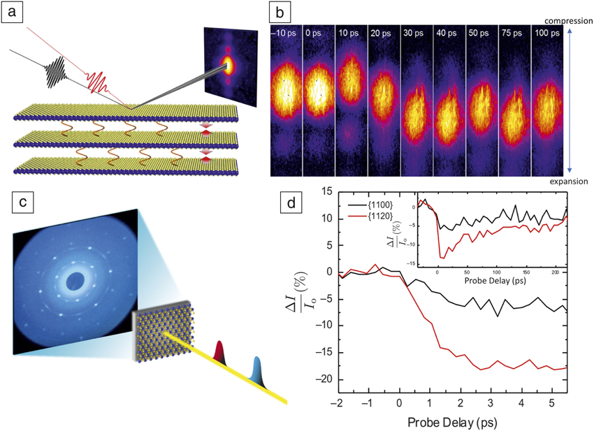
Ultrafast structural dynamics in quasi-2D materials. (a) Femtosecond x-ray scattering measurements probing light-induced interlayer coupling within a single-domain MoS2 exfoliated flake.Reference Mannebach, Nyby, Ernst, Zhou, Tolsma, Li, Sher, Tung, Zhou, Zhang, Seyler, Clark, Lin, Zhu, Glownia, Kozina, Song, Nelson, Mehta, Yu, Pant, Aslan, Raja, Guo, DiChiara, Mao, Cao, Tongay, Sun, Singh, Heinz, Xu, MacDonald, Reed, Wen and Lindenberg8 (b) Measurements of the center of mass of the scattered x-ray spot in a pump-probe geometry reveal an unexpected electronically induced compression appearing at time t =10 ps (shift of the center of mass to higher momentum transfer), associated with a light-induced modulation of the van der Waals interaction. (c) Femtosecond MeV electron scattering of monolayer MoS2 probing electron–phonon coupling and phonon transport processes with red pulse representing the pump laser pulse and blue pulse the femtosecond electron probe pulse.Reference Mannebach, Li, Duerloo, Nyby, Zalden, Vecchione, Ernst, Reid, Chase, Shen, Weathersby, Hast, Hettel, Coffee, Hartmann, Fry, Yu, Cao, Heinz, Reed, Dürr, Wang and Lindenberg9 These time scales are reflected in structure-factor modulations shown in (d) and (inset) in the relaxation of the photo-induced response, showing a few picoseconds electron–phonon coupling time scales followed by cooling of the monolayer into the supporting substrate within ∼100 ps. Note: I 0, the unperturbed diffracted intensity; ΔI, induced change in diffracted intensity.
From the electron-scattering perspective, major technological advances have occurred during the last 10 years, with adaptation of conventional instruments for ultrafast studies, refinement of pulse-compression schemes to mitigate the deleterious effects of space-charge broadening arising from electron–electron repulsion, and extension to relativistic energies enabling the generation of bright, sub-100-fs-duration electron pulses.Reference Plemmons, Suri and Flannigan10–Reference Otto, René de Cotret, Stern and Siwick12 Accordingly, one can retain coherence lengths and achieve spatial resolutions that allow for atomic-scale processes to be visualized on ultrafast time scales.
Correspondingly, time-resolved x-ray science has undergone a paradigm shift in recent years following the development of x-ray free-electron lasers, first at the Linac Coherent Light SourceReference Bostedt, Boutet, Fritz, Huang, Lee, Lemke, Robert, Schlotter, Turner and Williams13 and now at a number of other facilities around the world, with next-generation sources already under construction.14 At a basic level, these sources make use of a relativistic electron beam in conjunction with a periodic magnetic field to create periodic wiggling of the electron beam. Under resonant conditions, the radiated field from these oscillating electrons acts back on the electrons themselves and causes bunching that in turn leads to constructive interference in the radiated fields from each individual electron in a feedback loop, providing a giant boost in radiated power.Reference Kim, Huang and Lindberg15
General scattering methods for resolving ultrafast materials dynamics
In general, ultrafast materials dynamics can be visualized using both real-space (imaging) and reciprocal-space (diffraction) approaches. Such methods are highly complementary, providing structural (atomic) and morphological (nanoscale to microscale) information with femtosecond time resolution such that the evolution of a material—from the initial atomic-scale motions and rearrangements to the larger-scale propagation of energy and phase fronts—can be determined. In many cases, the myriad phenomena that occur within a material that has been rapidly driven from equilibrium, though interwoven to some extent, evolve on somewhat disparate time scales. For example, carrier–carrier scattering and electron–phonon coupling in a photoexcited semiconductor occur on the femtosecond to few-picosecond time scales, while subsequent phonon–phonon scattering and thermoelastic effects evolve over tens to hundreds of picoseconds. Accordingly, one can generate a comprehensive, spatiotemporally evolving picture of the dynamics by using multiple methods capable of accessing specific regions of the experimental parameter space.
Ultrafast electron and x-ray diffraction are used to probe the reciprocal-space dynamics of materials, thus providing information on the atomic-scale processes that occur following excitation.Reference Lindenberg, Johnson and Reis5,Reference Miller16 This is typically accomplished by quantifying the time-varying changes in scattering patterns. For example, such changes can be encoded in structure factors associated with the scattered intensity or by shifts in the position of Bragg peaks in reciprocal space, typically associated with local strains. In many cases, x-ray and electron-scattering approaches provide complementary information, as shown in Figure 1. Here, two recent experimentsReference Mannebach, Nyby, Ernst, Zhou, Tolsma, Li, Sher, Tung, Zhou, Zhang, Seyler, Clark, Lin, Zhu, Glownia, Kozina, Song, Nelson, Mehta, Yu, Pant, Aslan, Raja, Guo, DiChiara, Mao, Cao, Tongay, Sun, Singh, Heinz, Xu, MacDonald, Reed, Wen and Lindenberg8,Reference Mannebach, Li, Duerloo, Nyby, Zalden, Vecchione, Ernst, Reid, Chase, Shen, Weathersby, Hast, Hettel, Coffee, Hartmann, Fry, Yu, Cao, Heinz, Reed, Dürr, Wang and Lindenberg9 on quasi-two-dimensional transition-metal dichalcogenide materials demonstrate how one can access fundamental electron–phonon coupling time scales, explore interfacial phonon transport, and utilize unique means for manipulation of interlayer van der Waals bonding.
Figure 1a shows femtosecond x-ray pulses at the Linac Coherent Light Source diffracted from a single-domain MoS2 exfoliated flake following optical excitation with photon energies that are higher than the bandgap of the material. By measuring the center of mass of the scattered x-ray pulse, one can directly probe the time-dependent interlayer spacing, revealing a surprising light-induced compressive response at t = 10 ps, in which the layers are pushed together transiently, associated with electronic modulation of the van der Waals interaction. Here, the magnitude of the compression or expansion is encoded directly in the spatial position of the diffracted x-ray spot on the detector (Figure 1b). This approach is sensitive to strains at the parts-per-million level.Reference Kozina, Hu, Wittenberg, Szilagyi, Trigo, Miller, Uher, Damodaran, Martin, Mehta, Corbett, Safranek, Reis and Lindenberg17 Figure 1c–d shows corresponding MeV electron diffraction measurements that probe the same material but for an isolated single monolayer. Two different reflections are shown indexed by their Miller indices (Figure 1d), showing large-amplitude structure-factor modulations associated with the initial energy transfer from hot electrons to lattice degrees of freedom. As the lattice mean-square displacements start to increase as a result of this energy transfer, this induced disorder leads to a reduction in the relative intensity of the associated Bragg spots. The inset in Figure 1d shows the long-time relaxation behavior of this response, associated with thermal transport into the support layer of the MoS2 monolayer. All of these processes play crucial roles in the optoelectronic functionality of devices based on these materials.
By extending the general technical approach of ultrafast pump-probe experiments to conventional electron microscopy (scanning and transmission [SEM and TEM], respectively), the temporal resolutions of these critically important materials characterization tools can be greatly expanded, extending to the femtosecond time scale.Reference Zewail4,Reference King, Campbell, Frank and Reed18–Reference Adhikari, Eliason, Sun, Bose, Flannigan and Mohammed20 This is generally achieved by interfacing a femtosecond pulsed laser with an electron microscope, the column or housing of which has been modified to enable optical access to both the electron-gun region and to the specimen position. In this way, discrete packets of (probe) electrons can be generated via the photoelectric effect at the source, and dynamics within the specimen can be induced (pumped) via coherent photoexcitation. Varying the arrival time of the probe electron packets and pump photon pulses at the specimen with a mechanical delay stage allows for the dynamics occurring during a select time range to be stroboscopically resolved.
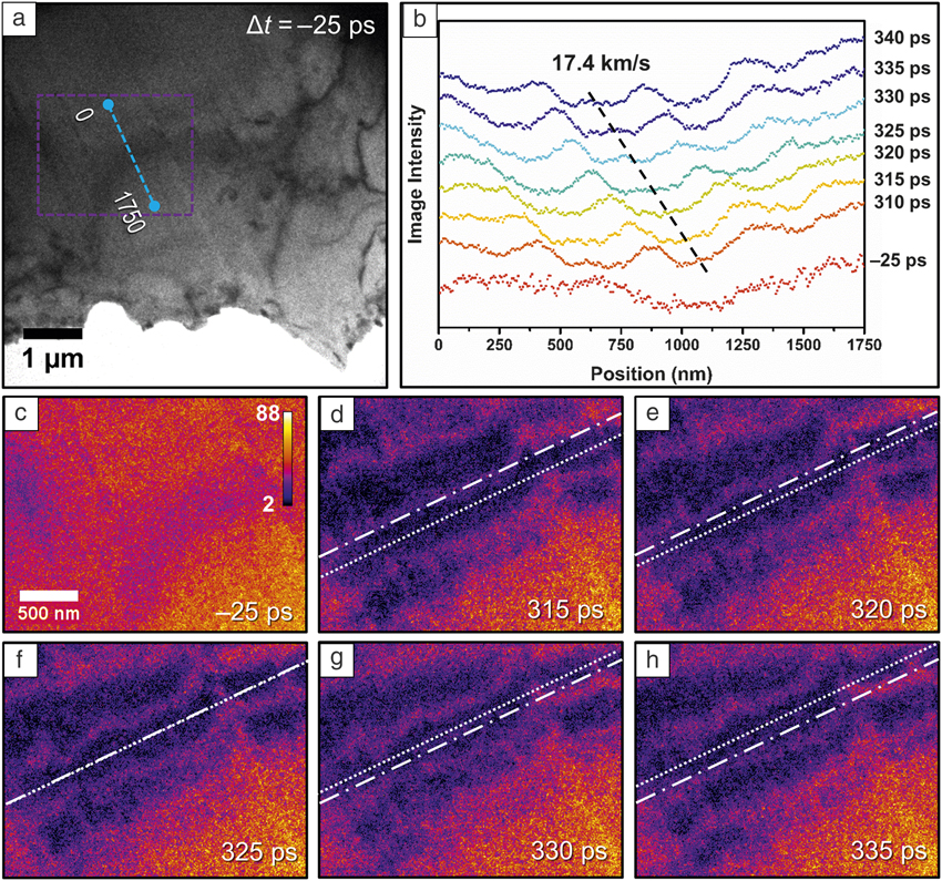
Such lab-scale instruments are especially powerful, as they allow for the all-in-one study of ultrafast materials processes with the many techniques of electron microscopy (e.g., imaging, diffraction, spectroscopy). For example, with femtosecond electron imaging, the spatiotemporal behaviors of coherent, nanoscale strain-wave dynamics in a variety of materials have been directly visualized, and femtosecond electron energy-loss spectroscopy has been used to resolve dynamics associated with both valence– and core–shell excitations.Reference Cremons, Plemmons and Flannigan21–Reference van der Veen, Penfold and Zewail24 Figure 2 shows the imaging of coherent, photoexcited hypersonic strain waves propagating through a single crystal of undoped Ge on the picosecond time scale. Because the contrast-forming mechanisms in TEM are extremely sensitive to changes in lattice orientation with respect to the incoming (probing) electrons, the low-energy (few meV) strains cause enough of a local deformation to appear as dark bands traveling within the plane of the crystal. By tracking those bands in time, the behaviors (direction, velocity, dispersion) can be quantified and monitored with respect to material morphology and structure. Such studies extend the time scales accessible with electron microscopy by ten orders of magnitude compared to fast digital detectors, opening the way to a wide range of ultrafast atomic-scale studies on, for example, elastic responses, transport processes, phase-change behaviors, and the roles of defects on nonequilibrium phenomena.
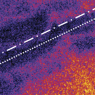
Ultrafast electron imaging of directional, hypersonic strain waves in single-crystal Ge.Reference Cremons, Du and Flannigan22 (a) Bright-field ultrafast electron microscope image of the Ge specimen 25 ps prior (Δt) to femtosecond photoexcitation. The analyzed region of interest is outlined, with the length denoted (1750 nm). (b) Time-varying image intensity along the length noted in panel (a). The time window shows spans 310 to 340 ps after photoexcitation, and the propagation of one strain wave is marked by the dashed line, indicating a phase velocity of 17.4 km/s. (c–h) Select false-colored images of the strain-wave motion within the region of interest from 315 to 335 ps. The dot-dashed line marks the initial wavefront position, while the dotted line across the center of the wavefront denotes its motion. The first panel is an image of the region of interest 25 ps prior to excitation and is included for comparison. The color bar is in units of raw-image counts.Reference Mannebach, Nyby, Ernst, Zhou, Tolsma, Li, Sher, Tung, Zhou, Zhang, Seyler, Clark, Lin, Zhu, Glownia, Kozina, Song, Nelson, Mehta, Yu, Pant, Aslan, Raja, Guo, DiChiara, Mao, Cao, Tongay, Sun, Singh, Heinz, Xu, MacDonald, Reed, Wen and Lindenberg8
In this issue
This issue of MRS Bulletin contains five articles that discuss the visualization of ultrafast atomic to microscale materials dynamics via scattering methods. The methods and approaches developed and employed by each of the authors span the range of electron- and x-ray-based ultrafast methods currently being used to uncover new fundamental physical insights into transient materials behaviors. In addition to these methods, the many discoveries generated by them have greatly expanded our understanding of the intricate, complex, and often hard-to-predict ways in which materials respond on very short time scales when driven away (and, at times, far) from equilibrium.
The article by Horn-von HoegenReference Horn-von Hoegen25 describes recent measurementsReference Frigge, Hafke, Witte, Krenzer, Streubühr, Samad Syed, Mikšić Trontl, Avigo, Zhou, Ligges, von der Linde, Bovensiepen, Horn-von Hoegen, Wipperman, Lücke, Sanna, Gerstmann and Schmidt26 using femtosecond electron bunches in a reflection high-energy electron diffraction geometry to probe how atoms move on a surface. In this work, a light-induced insulator-to-metal transition is observed in a single atomic layer of indium wires, with the surface reconstruction changing on subpicosecond time scales. The transition to the nonequilibrium structure occurs in a coherent fashion, in which each indium atom moves in a spatially coherent manner. Interestingly, the relaxation of this excited state is observed to be much longer (on the order of nanoseconds) than the cooling time associated with thermal transport into the substrate. This effect is attributed to the presence of an energy barrier separating the excited and equilibrium phases, therefore indicating the formation of a transient supercooled state. Such approaches represent a new means for probing the nonequilibrium kinetics of surface-mediated processes.
The article by TrigoReference Trigo27 presents a new time-domain inelastic x-ray scattering approach for probing phonon excitations in materials in a momentum (q)-resolved fashion. This enables, for example, the measurement of nonequilibrium phonon-dispersion relations and q-resolved phonon-relaxation processes.Reference Jiang, Trigo, Fahy, Murray, Savić, Bray, Clark, Henighan, Kozina, Chollet, Glownia, Hoffmann, Zhu, Delaire, May, Sales, Lindenberg, Zalden, Sato, Merlin and Reis28,Reference Trigo, Fuchs, Chen, Jiang, Cammarata, Fahy, Fritz, Gaffney, Ghimire, Higginbotham, Johnson, Kozina, Larsson, Lemke, Lindenberg, Ndabashimiye, Quirin, Sokolowski-Tinten, Uher, Wark, Zhu and Reis29 This approach focuses on the diffuse x-ray scattering between the Bragg peaks as a means of performing inelastic x-ray scattering with energy spread larger than the associated phonon energies. In particular, at a specific wave vector q defined by a pixel on an x-ray area detector, one measures the time-dependent light-induced oscillatory response, thus defining the phonon-dispersion relation (e.g., the frequency as a function of phonon momentum). Trigo shows how this approach, termed Fourier transform inelastic x-ray scattering (FTIXS), can be used to visualize phonon decay channels and probe anharmonic phonon–phonon coupling in potentially new ways.
The varied conventional electron microscopy techniques that have been extended to the femtosecond regime also include methods for probing the connection between charge carriers and material structure and morphology. This is especially the case for femtosecond electron energy-loss spectroscopy (fs-EELS) and scanning ultrafast electron microscopy (SUEM).Reference Adhikari, Eliason, Sun, Bose, Flannigan and Mohammed20,Reference Carbone, Kwon and Zewail23 In their article,Reference Pomarico, Kim, García de Abajo, Kwon, Carbone and van der Veen30 Pomarico et al. describe the exciting developments occurring with fs-EELS, including ultrafast valence and core-loss dynamics, the direct imaging of coherent, low-energy plasmonic resonances and decay dynamics at surfaces and interfaces, and the recent development of nanosecond, single-shot EELS.Reference Picher, Bucker, LaGrange and Banhart31 In conventional core-loss EELS experiments, energy losses due to excitation/ionization of core-level electrons can be used to identify the local composition and oxidation states of elements. Additionally, the fine structure near the main spectral features contains a wealth of information pertaining to, for example, local bonding conditions. The authors describe how translating these methods to the ultrafast regime can bring to light the transient nature of such chemical processes and can also reveal the impact of electron–photon interactions on core-level dynamics.Reference van der Veen, Penfold and Zewail24 The authors describe new developments in high-energy-resolution applications and direct monitoring of surface plasmon polariton dynamics using femtosecond energy-filtered imaging via photon-induced near-field electron microscopy.Reference Barwick, Flannigan and Zewail32,Reference Pomarico, Madan, Berruto, Vanacore, Wang, Kaminer, García de Abajo and Carbone33
In their article,Reference Yang, Liao and Mohammed34 Yang et al. describe an emerging ultrafast variant of scanning electron microscopy (SUEM).Reference Adhikari, Eliason, Sun, Bose, Flannigan and Mohammed20,Reference Yang, Mohammed and Zewail35 Though currently employed in only a few labs, the authors—pioneers of the technology and leaders in the field of ultrafast electron imaging—describe in detail the capabilities and future directions of this exciting approach. Significant impact has already been made with SUEM in the area of photoactive materials for electron–hole dynamics at surfaces and heterostructure interfaces. Owing to the imaging capabilities, the spatiotemporal response of charge carriers to photoexcitation, especially in the presence of structural inhomogeneities and abrupt morphological variations, can be directly visualized. As detailed in the article, new insights into the behavior of materials as varied as surface-terminated silicon, black phosphorus, semiconductor nanowires, and quantum dot arrays have already been generated with SUEM.
In addition to the real-space femtosecond electron imaging methods previously discussed, whether bright/dark field or energy filtered, another powerful approach for resolving local, nanoscale structural dynamics is ultrafast convergent-beam electron diffraction.Reference Yurtsever and Zewail36,Reference Feist, da Silva, Liang, Ropers and Schaefer37 In conventional (i.e., nonaberration-corrected) TEM, the illumination lens arrays and powerful objective lens enable formation of subnanometer-sized electron probes, which can be used to precisely probe nanoscale specimen regions. Additionally, the range of incident electron wave vectors owing to the converged geometry provides simultaneous access to multiple Laue zones, thus revealing three-dimensional crystallographic information within a single scattering pattern. Feist et al. are leading the way via the development of high-coherence femtosecond electron pulses in otherwise conventional transmission electron microscopes, as well as within table-top ultrafast low-energy electron diffraction (ULEED) scattering chambers. In their article,Reference Feist, Storeck, Schäfer and Ropers38 they describe their approaches to generating femtosecond electron pulses of high spatial and temporal coherence—in addition to nanometer-scale probe sizes—via side illumination of sharp metallic tips (e.g., a Schottky field-emission electron gun in a modified transmission electron microscope), which they use to conduct detailed spatially resolved studies of strain-wave dynamics in a graphite single crystal. Further, the authors describe highly sensitive measurements conducted on order/disorder transitions of various surface charge-ordering and associated lattice-deformation states in strongly electron-correlated materials (e.g., TaS2).
Finally, we feel it is important to note that the pace of instrument development and advancement for ultrafast imaging of materials dynamics has rapidly increased during the last 10 years.Reference Weathersby, Brown, Centurion, Chase, Coffee, Corbett, Eichner, Frisch, Fry, Guehr, Hartmann, Hast, Hettel, Jobe, Jongewaard, Lewandowski, Li, Lindenberg, Makasyuk, May, McCormick, Nguyen, Reid, Shen, Sokolowski-Tinten, Vecchione, Vetter, Wu, Yang, Durr and Wang11,Reference Qiu, Ha, Jing, Baryshev, Reed, Lau and Zhu39 The new free-electron laser LCLS-II, being constructed at the SLAC National Accelerator Laboratory, will be the world’s brightest x-ray laser and will significantly expand the accessible materials dynamics parameter space.14 Ultrafast electron microscopy has matured to the point where companies now offer commercially available instruments and solutions. One aspect of this is described in a recent article by Verhoeven et al.Reference Verhoeven, van Rens, Kieft, Mutsaers and Luiten40 The authors describe a method for generating picosecond pulses of electrons in a TEM by incorporating a compact resonant microwave cavity into the column. Using the large-amplitude fields generated when operating the cavity at its resonance frequency, the incident electron beam can be rapidly swept across a small slit. The resulting pulse train has a repetition rate matching the cavity frequency (e.g., 75 MHz) while maintaining the coherency of the continuous beam. Developments such as these are especially exciting,Reference Qiu, Ha, Jing, Baryshev, Reed, Lau and Zhu39–Reference van Rens, Verhoeven, Franssen, Lassise, Stragier, Kieft, Mutsaers and Luiten41 as they circumvents the need for using a pulsed laser to generate the probe photoelectron pulses, thus solving several practical challenges associated with spatial laser-beam stability and alignment at the electron source.
Summary
The advent of methods capable of probing the ultrafast structural response of materials from the atomic (quantum) to the mesoscale (continuum) has led to an explosion in increased understanding and new physical insights. While a single issue composed of a range of articles spanning this field falls well short of a comprehensive overview, it is our hope that the reader is at least left with a sense of the incredibly interesting and exciting science and engineering that has emerged in recent years. For those in the field, the future is especially exciting, as capabilities continue to expand and discoveries in an enormous variety of materials and systems continue to be made. Perhaps most importantly, new observations and physical insights enabled by advances in instrumentation will allow for the formulation of questions that previously would not have been answerable with existing approaches. This, therefore, naturally forms a connection with theory, allowing various frameworks and calculations to be directly tested with experiments. We hope the enthusiasm and the excitement surrounding the efforts to date is clear after reading this issue. As the development of new capabilities accelerates, we are filled with great anticipation for what is yet to come.
Acknowledgments
D.J.F. acknowledges support in part by the US Department of Energy, Office of Science, Office of Basic Energy Sciences under Award No. DE-SC-0018204, and in part by the Arnold and Mabel Beckman Foundation through a Beckman Young Investigator Award. A.M.L. acknowledges support by the US Department of Energy, Office of Science, Basic Energy Sciences, Materials Sciences and Engineering Division, under Contract DE-AC02–76SF00515.
David J. Flannigan is an associate professor of chemical engineering and materials science and a McKnight Presidential Fellow at the University of Minnesota. He received his BS and PhD degrees in chemistry from the University of Minnesota and the University of Illinois at Urbana-Champaign, respectively. He was a postdoctoral scholar at the California Institute of Technology. His research focuses on the study of atomic to mesoscale materials dynamics with in situ and ultrafast electron imaging, diffraction, and spectroscopy. His awards include a Beckman Young Investigator Award, an NSF CAREER Award, and a DOE Early Career Award. He is the recipient of a McKnight Land-Grant Professorship and the George W. Taylor Career Development Award at the University of Minnesota. Flannigan can be reached by email at flan0076@umn.edu.

Aaron M. Lindenberg is an associate professor at Stanford University with joint appointments in the Department of Materials Science and Engineering and the Department of Photon Science at SLAC. He received his BA degree from Columbia University in 1996, and his PhD degree in physics from the University of California, Berkeley, in 2001. He was named a Faculty Fellow at Berkeley from 2001 to 2003, and was a staff scientist at the SLAC National Accelerator Laboratory from 2003 to 2007. His awards include the DARPA Young Faculty Award, the Department of Energy Outstanding Mentor Award, and the Alfred Moritz Michaelis Prize. He was named a Terman Fellow and a Chambers Faculty Scholar at Stanford and an I.I. Rabi Scholar at Columbia. Lindenberg can be reached by email at aaronl@stanford.edu.


