

Disruptive technology in photovoltaics
Photographic films containing light-sensitive silver halides dominated photography until the early 21st century, but now have vanished from the market because of digital technology. The latter is termed a “disruptive technology.” The question is why and how technology disruption occurs. According to the theory of diffusion of innovations, which explains an epidemic-like spreading of new ideas and technologies,Reference Rogers1 existing technology tends to undergo four stages of change—early adoption, rapid growth, maturity, and decline. At the maturity stage, typically, a new innovation is initiated that coexists with the old technology, but the transition is not continuous. In the early stages of the innovative technology, its performance and value are lower than the existing technology. However, the new technology eventually improves performance via breakthroughs, gains better value, and quickly disrupts the previous technology.
How can we be aware of such technology disruption? We need a symptom that indicates technology disruption. In a chemical reaction, the reactant experiences and overcomes a transition state to be converted to the final product. For instance, to synthesize ethyl alcohol from bromoethane, the entering hydroxyl anion and the exiting bromide coexist at the high-energy transient state. In technology disruption, a hybrid state, similar to the transition state in a chemical reaction, is expected. For example, a hybrid car using both gasoline and electricity represents the transition from the internal combustion engine vehicle to an electric vehicle, where the latter is the innovative new technology. In the field of energy, we currently use fossil fuels, which have caused a change in the climate due to massive carbon dioxide emissions. This will be disrupted by renewable energy, where emerging hybrid electricity uses renewable energy as an innovative technology.
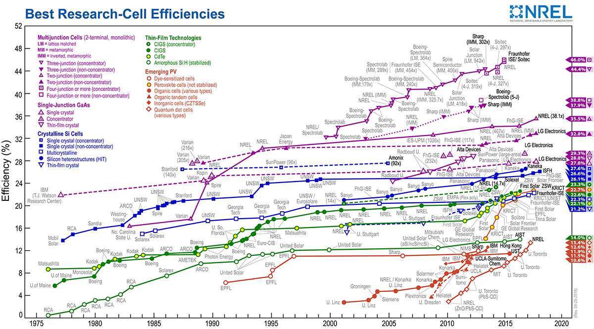
Solar cells represent a promising renewable energy source. Silicon-based solar cells currently dominate the photovoltaic (PV) market. However, silicon solar cells will likely be replaced with perovskite solar cells (PSCs) in the near future, with the intermediate step of the introduction of hybrid tandem solar cells and PSCs as the innovative technology. Because of lower costs and high power-conversion efficiencies (PCEs), with a certified value of 22.7% already surpassing the values for polycrystalline silicon and thin-film solar cells (22% ≤ PCE ≤ 22.7%),2 PSCs are regarded as a disruptive technology in PVs.
According to the PV learning curve (average PV module price versus cumulative installation power of the PV module) in the International Technology Roadmap for Photovoltaics,3 the calculated worldwide installed PV module power reached 402 GW at the end of 2017. This represents an increase of 100 GW as compared to the capacity of 303 GW in 2016. The PV module price, which is an average price for Si based modules, was USD$0.37/Wp (Watt peak) in 2016, which was further reduced to USD$0.34/Wp in 2017. This indicates that renewable energy disruption has already started. The US Energy Information Administration reported in its Annual Energy Outlook in 2017 that the cost of electricity from PV power will be cheaper than that from nuclear power in 2022.4 PV power is expected to dominate the energy market in the future.
Organic–inorganic halide perovskites
There are numerous materials used for solar-cell technologies, including the well-known Si, Cu(In, Ga)Se2 (CIGS), and CdTe, for which PV performances have increased slowly. Compared to these conventional solar-cell materials, the PCE of solar cells based on organic–inorganic halide perovskites has increased rapidly from 3.8% in 2009 to 22.7% in 2017.5 The latest PCE of PSCs (22.7%) is even higher than those of the conventional solar cells (22.6% from CIGS, 22.3% from poly Si, and 22.1% from CdTe).2
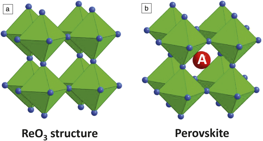
Perovskites have a crystalline structure with chemical formula ABX3, where X is a halogen (or oxygen) anion, and A and B are cations coordinated with 12 anions and six anions, respectively. For lead halide perovskites, Pb sits in the B site and a halide sits in the X site. The corner-sharing Pb-I three-dimensional (3D) octahedra, which basically form the ReO3 structure, provide cubooctahedral sites for A cations (Figure 1). If an organic ammonium ion such as methylammonium (MA) or formamidium (FA) is included in the A site, the optoelectronic and physical properties of the materials become different from those of conventional oxide-based semiconductors. For instance, conductivity increases with temperature in the case of conventional semiconductors, whereas conductivity decreases with temperature in APbI3 (A = MA, FA, or mixed MA and FA). Thus, we need to study halide perovskites with organic cations using a different approach than that used for conventional semiconductor physics.
(a) ReO3 structure showing corner-sharing ReO6 octahedra. (b) Perovskite structure showing an A cation in a cubooctahedral cage in the ReO3 backbone.
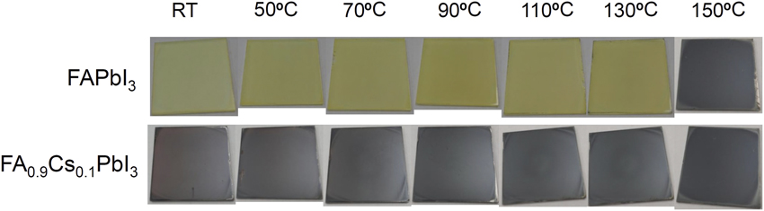
MAPbI3 is tetragonal, and FAPbI3 has a pseudo-cubic structure. Tetragonal MAPbI3 can be stabilized at room temperature, but it is difficult to form FAPbI3 with a perovskite structure at low temperature (<150°C). Low-temperature-annealed FAPbI3 is stabilized in a one-dimensional (1D) hexagonal structure. If FA is partly substituted by cesium ions, a 3D perovskite phase can be stabilized, even at room temperature (Figure 2).Reference Lee, Kim, Kim, Seo, Cho and Park6
Digital photographs of FAPbI3 and FA0.9Cs0.1PbI3 before and after annealing. (Top) FAPbI3 film where film color depends on annealing temperature. (Bottom) With the substitution of 10 mol% Cs for FA, FAPbI3 films stabilize at temperatures lower than 150°C. Note: FA, formamidium; RT, room temperature.Reference Lee, Kim, Kim, Seo, Cho and Park6
Organic–inorganic lead halide perovskites are known to be defect tolerant, different from conventional photovoltaic materials such as GaAs and CdSe that exhibit defect-intolerant properties. In the former (APbX3), the defect states reside within the conduction band (CB) and valence band (VB) with the CB and VB composed of Pb(6p)-I(5p) antibonding and Pb(6s)-I(5p) antibonding states respectively.Reference Kovalenko, Protesescu and Bodnarchuk7 Because the bandgap is free of nonbonding states, APbX3 is defect tolerant, unlike GaAs and CdSe, which have bandgaps that have nonbonding states that act as charge traps.
Methylammonium lead iodide received little attention over the years, until the report of its use in a high-efficiency, stable solid-state PSC in 2012.Reference Kim, Lee, Im, Lee, Moehl, Marchioro, Moon, Humphry-Baker, Yum, Moser, Grätzel and Park8 Prior to the development of solid-state PSCs, perovskites were used as sensitizers in liquid-junction-type solar cells, yielding efficiencies of 3.8%Reference Kojima, Teshima, Shirai and Miyasaka9 (2009) and 6.5% (2011).Reference Im, Lee, Lee, Park and Park10 Not much attention was paid to these perovskite sensitizers due to the instability of perovskites in liquid electrolytes. Nevertheless, the report demonstrating 6.5%Reference Im, Lee, Lee, Park and Park10 contained an important message regarding the concentration of the perovskite precursor solution. As compared to the unsuccessful preparation of the perovskite phase from the low concentration (8 wt%) of the precursor solution (reported in Reference Kim, Lee, Im, Lee, Moehl, Marchioro, Moon, Humphry-Baker, Yum, Moser, Grätzel and ParkReference 8), we could reproducibly prepare the perovskite phase from solutions with concentrations as high as 40 wt%.Reference Im, Lee, Lee, Park and Park10 This corresponds to approximately 1.2 M (molar concentration), which indicates that the ionic strength is important in preparing the perovskite phase. In highly concentrated solutions, iodoplumbate or 1D chain colloids are likely to form, leading to high-quality perovskites for high-efficiency solar cells. Moreover, the absorption coefficient of MAPbI3 was found to be one order of magnitude higher than that of a ruthenium-based dye (N719).Reference Im, Lee, Lee, Park and Park10 Based on this, successful fabrication of high-efficiency solid-state PSCs was realized by decreasing the thickness of TiO2 films, where the thickness of the region in which light absorption takes place is inversely proportional to the absorption coefficient.Reference Kim, Lee, Im, Lee, Moehl, Marchioro, Moon, Humphry-Baker, Yum, Moser, Grätzel and Park8
The number of publications on PSCs has been increasing exponentially since 2012, with more than 3000 peer-reviewed articles published in 2017 alone. Thus, 2012 represents an inflection point for publications on perovskites, including oxide-, chalcogen-, and halide-based ones, which indicates that the development of solid-state perovskite solar cells triggered the initial interest in perovskite photovoltaics.
Progress of PSC at Sungkyunkwan University
After the initial work on solid-state PSCs reported in 2012 by the Park group at Sungkyunkwan University (SKKU), researchers have continued efforts into developing high-efficiency PSCs and understanding the fundamentals of the materials and devices. Here, important progress in PSCs at SKKU is described.
Grain size–photoluminescence relation
We developed a method to control the grain size of MAPbI3 perovskites via a two-step spin-coating procedure, where the grain size tends to increase with decreasing concentration of the methylammonium iodide (MAI) solution, as shown in Figure 3a.Reference Im, Jang, Pellet, Grätzel and Park11 Large grains are better than small grains for PCE, mostly due to the higher short-circuit current density (J sc) associated with the light-scattering effects (Figure 3b). Large grains more effectively scatter red light, which enhances the external quantum efficiency for long wavelengths, thus leading to higher PCE. However, further increase in the grain size did not improve J sc, which may be related to inducing more defects as grain size increases; the optimum grain size is approximately 700 nm. The micrometer-size crystals (Figure 3c) show less bright photoluminescence (PL) than the submicrometer-size ones (Figure 3d) due to nonradiative recombination trap states.Reference Mastroianni, Heinz, Im, Veurman, Padilla, Schubert, Würfel, Grätzel, Park and Hinsch12 This reveals the importance of grain size in minimizing nonradiative recombination.
(a) MAPbI3 grain size as a function of methylammonium iodide (MAI) concentration ranging from 0.032 M to 0.063 M. The grain size exponentially decays with MAI concentration. (b) Light-harvesting efficiency dependence on MAI concentration showing an increase in internal scattering in the green-red region as the MAI concentration decreases. Micro-PL for MAPbI3 crystals prepared from (c) 0.032 M and (d) 0.044 M MAI solution. PL intensity is strong and homogeneous for 0.044 M, which is related to high photocurrent density, while PL intensity is low and inhomogeneous for 0.032 M, even for larger grain sizes, which is responsible for low photocurrent density.Reference Im, Jang, Pellet, Grätzel and Park11,Reference Mastroianni, Heinz, Im, Veurman, Padilla, Schubert, Würfel, Grätzel, Park and Hinsch12

Nonstoichiometric adduct approach for passivating grain boundaries
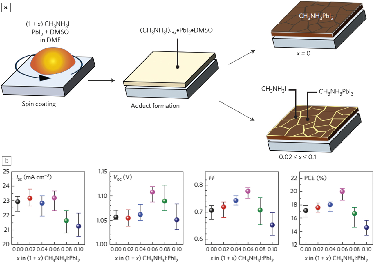
How can we prepare perovskite films with the appropriate grain size to minimize defects? The Lewis acid-base adduct approach was proposed as one of the most reproducible and reliable ways to achieve high-performance PSCs.Reference Ahn, Son, Jang, Kang, Choi and Park13 The main drawback in solution-based processes is that grain boundaries inevitably form in perovskite films. Because grain boundaries can act as recombination sites, passivation of the grain boundaries is required. Passivation can be achieved by utilizing the adduct approach. Excess MAI is introduced into the precursor solution by depositing unreacted excess MAI onto the surface of the perovskite crystals. Therefore, this method is termed the nonstoichiometric adduct approach, as shown in Figure 4a. A certain amount of excess MAI maximizes the fill factor ([FF], ratio of (J max × V max) to (J sc × V oc), where J max and V max represent the photocurrent and voltage at maximum power, respectively, and V oc is the open-circuit voltage) and V oc, leading to PCE of more than 20% (Figure 4b).Reference Son, Lee, Choi, Jang, Lee, Yoo, Shin, Ahn, Choi, Kim and Park14 Moreover, grain-boundary engineering was found to increase the carrier lifetime of bulk perovskite materials, separate charge effectively, and enhance charge conductance.
(a) Grain-boundary healing process via nonstoichiometric adduct method, where excess MAI (=CH3NH3I) was introduced to the precursor solution. (b) Photovoltaic parameters as a function of MAI concentration (x), where the open-circuit voltage (V oc) and fill factor (FF) were maximized at x = 0.06 without sacrificing the short-circuit current density (J sc).Reference Son, Lee, Choi, Jang, Lee, Yoo, Shin, Ahn, Choi, Kim and Park14 Note: DMF, dimethylformamide; DMSO, dimethylsulfoxide; PCE, power-conversion efficiency; MA, methylammonium; MAI, methylammonium iodide.
As compared to MAPbI3, FAPbI3 may be more useful because of its lower bandgap that can generate higher photocurrents. We reported a FAPbI3 perovskite solar cell with PCE as high as 16% in 2014,Reference Lee, Seol, Cho and Park15 where an ion-exchange reaction was developed to introduce a thin overlayer on top of the FAPbI3 layer. Although the photostability of FAPbI3 is better than that for MAPbI3, we found that FAPbI3 can be still unstable, especially under humidity. We proposed a solution to this problem by substituting FA with smaller cesium ions (FA0.9Cs0.1PbI3), which eventually led to improved moisture stability and reduced J–V hysteresis.4
Modification of the perovskite morphologies is one of the many challenging issues for PSCs. We developed two-dimensional (2D) nanowire perovskites for the first time using a two-step spin-coating process, where MAPbI3 nanowires grew when small amounts of polar aprotic solvents such as DMSO (dimethylsulfoxide) were added to the MAI/IPA (isopropanol) solution.Reference Im, Luo, Franckevicius, Pellet, Gao, Moehl, Zakeeruddin, Nazeeruddin, Grätzel and Park16 Nanowires of MAPbI3 showed better lateral conductivities and longer carrier lifetimes than their 3D cuboid counterparts.
Interfacial engineering using 2D perovskites
Despite the superb photovoltaic performance of PSCs, there remain many issues to be solved, such as long-term stability, J–V hysteresis, and lead toxicity. Regarding toxicity, the actual amount of lead in PSCs was calculated to be comparable to naturally occurring amounts.Reference Park, Grätzel, Miyasaka, Zhu and Emery17 Further, the lead can be recovered by acid treatment, and PbI2, which is generated as a product of decomposition of PSCs, is rather insoluble in pure water at 25°C. Nevertheless, care should be taken not to release lead ions into the environment.
J–V hysteresis is a critical issue in PSCs. Devices with severe hysteresis, which indicates the presence of many defects in the perovskite, showed poor stability.Reference Park, Grätzel, Miyasaka, Zhu and Emery17 It is thus important to understand the origin of hysteresis in PSCs. Detailed studies using impedance spectroscopy revealed that the selective contact/perovskite interfaces play a crucial role, where the selective contact is an electron transporting layer (e.g., TiO2) or a hole transporting layer (2,2′,7,7′-tetrakis-[N,N-di-4-methoxyphenylamino]-9,9′-spirobifluorene, [spiro-MeOTAD]). Normally, a mesoscopic structure (10 nm ∼ 100 nm) is composed of transparent conductive oxide (TCO)/compact TiO2/mesoporous TiO2/perovskite/spiro-MeOTAD/Au. These impedance studies showed that the TiO2/perovskite interface has a larger influence on the hysteresis as compared to the spiro-MeOTAD/perovskite interface.Reference Kim, Jang, Ahn, Choi, Guerrero, Bisquert and Park18 Replacing TiO2 and spiro-MeOTAD with phenyl-C61-butyric acid methyl ester (PCBM) and poly(3,4-ethylenedioxythiophene) poly(styrene sulfonate) (PEDOT:PSS), respectively, is one method to reduce the hysteresis, but doing so reduces the PCE.
The highest PCE (22.7%) has been achieved from mesoscopic structures that include a TiO2 layer; it is therefore necessary to find a methodology that removes the hysteresis-inducing structures. Interfacial engineering is considered to be the approach with the most potential to reduce hysteresis. Since it has been proposed that ion migration is involved in the evolution of hysteresis,Reference Chen, Yang, Zheng, Wu, Li, Yan, Bisquert, Garcia-Belmonte, Zhu and Priya19 we considered inserting a 2D perovskite between 3D perovskite grains. Ion migration is likely to be significantly reduced in a 2D structure because the intralayer Pb–I bond is expected to be stronger than that in the 3D structure. Figure 5a shows that insertion of (PEA)2PbI4 (PEA = phenyl ethyl ammonium) at the grain boundaries of MAPbI3 greatly reduces the hysteresis and also improves the stability.Reference Chen, Lee and Park20 The activation energy for iodide migration was calculated to be higher for 2D perovskites than for 3D perovskites, and this was responsible for both reduced hysteresis and improved stability.
(a) (i) Passivation of MAPbI3 grain boundaries by insertion of 2D (PEA)2PbI4. J–V curves of (ii) MAPbI3 and (iii) 2D modified MAPbI3. Red and black lines represent reverse (from V oc to J sc direction) scanned and forward (from J sc to V oc direction) scanned data, respectively. (iv) PCE with aging time for devices with MAPbI3 before (black data) and after modification with 2D perovskite (blue data). Insertion of 2D perovskite at grain boundaries of 3D perovskite reduced the hysteresis and improved long-term stability. (b) In situ formation of 2D (5-AVAI)2PbI4 interlayer between perovskite and CuSCN. (i) Schematic process for preparing in situ formed 2D interlayer on perovskite film, where excess PbI2 was introduced in the precursor solution to form unreacted PbI2 on the perovskite surface. The surface PbI2 reacted with 5-AVAI to form 2D perovskite. (ii) (Left) Micrograph and (right) schematic structure of 2D ((5-AVAI)2PbI4) perovskite. (iii) J–V curves showing reduced hysteresis after the introduction of a 2D interlayer between CuSCN and perovskite. Red and black lines show the reverse scanned data, while pink and gray lines represent the forward scanned data. The 2D interlayer played an important role in reducing hysteresis.Reference Chen, Lee and Park20,Reference Chen, Seo and Park21 Note: MA, methylammonium; PEA, phenyl ethyl ammonium; AVAI, ammonium valeric acid iodide; PCE, power-conversion efficiency; J, current density; FTO, fluorine-doped tin oxide; FA, formamidium; IPA, isopropanol.

Because both grain boundaries and interfaces are important in terms of hysteresis and stability and we found that grain-boundary engineering reduced hysteresis, interface engineering was investigated to determine its effect on hysteresis. A similar method to that previously mentioned was applied to the perovskite/hole transport layer. Insertion of (5-AVAI)2PbI4 (5-AVAI = 5-ammonium valeric acid iodide) between the perovskite and CuSCN layer reduces hysteresis significantly (Figure 5b), where the 2D interlayer was formed in situ by dripping the 5-AVAI solution onto the annealed perovskite film.Reference Chen, Seo and Park21 Interfacial engineering is thus confirmed to be an effective means of reducing hysteresis and at the same time, improving stability. However, even after introduction of the 2D interlayer, hysteresis effects still remain to some extent. This is indicative of the presence of bulk defects in perovskite films, which are probably located near selective contacts and affect hysteresis behavior.
Universal approach for hysteresis-free PSCs
The addition of small amounts of KI to the precursor solution was found to generate hysteresis-free PSCs with a normal mesoscopic layout and a mesoporous TiO2 layer.Reference Son, Kim, Seo, Lee, Lee, Shin and Park22 This works universally for perovskite materials with different compositions such as pure MAPbI3, FAPbI3, dual-cation, and triple-cation perovskites. Among the tested alkali metal cations (Li+, Na+, K+, Rb+, and Cs+), only K+ worked effectively in removing the hysteresis (see Figure 6). Potassium ions are expected to be in the lattice based on x-ray diffraction studies. Electrode polarization was also reduced by the addition of KI. Also, the trap density decreased after KI addition, which is indicative of a reduction in bulk defects.
(a) (Left) Removal of Frenkel defect by (right) insertion of KI in octahedrally coordinated interstitial sites, (b) (left to right) showing removal of current density–voltage (J–V) hysteresis. Red data represent forward scanning and black data represent reverse scanning. (c) Effect of alkali metal ions (Li+, K+, and Cs+) on the hysteresis showing that only K+ ions work effectively. Gray and red represent forward scanned data and black and green represent reverse scanned data.Reference Chen, Seo and Park21 Note: VI, vacancy at I site; MA, methylammonium.

To elucidate the effects of KI, density functional theory calculations were performed.Reference Son, Kim, Seo, Lee, Lee, Shin and Park22 Before the KI treatment, the iodide in pristine perovskite diffuses from Pb–I–Pb sites toward interstitial sites, forming Pb–Pb dimers. This is a Frenkel defect, which acts to trap charges, thereby causing J–V hysteresis (Figure 6). Removal of such Frenkel defects is therefore expected to eliminate hysteresis. How can potassium ions remove Frenkel defects? Since the interstitial site for the Frenkel defects has octahedral coordination, potassium, which has a coordination number of six based on the cation/anion radius ratio, can occupy this site.
Beyond PVs: X-ray imaging and light-emitting diodes
Organic–inorganic perovskites have other potential applications in optoelectronic devices such as in light-emitting diodes (LEDs), resistive memories, and photodetectors, indicating that perovskites are multifunctional materials. We demonstrated the fabrication of a perovskite LED with external quantum efficiency of 8.21%, the second best value obtained at the time, and current efficiency of 34.46 cd/A, realized using the nonstoichiometric adduct method and a solvent-vacuum annealing process.Reference Lee, Choi, Yang, Ham, Jeon, Lee, Song, Ji, Yoon, Seo, Shin, Han, Jung, Kim and Park23 Recently, we fabricated an x-ray imaging system using microcrystalline MAPbI3 as the photodetector.Reference Kim, Kim, Son, Jeong, Seo, Choi, Han, Lee and Park24 Low-dose x-ray imaging technology is crucial for diagnosis and therapy. For this purpose, a highly sensitive x-ray photodetecting material is required. Between the direct and indirect x-ray imaging processes, MAPbI3 was applied to the direct method, which involves directly attaching the photodetector onto the readout backplane thin-film transistor array. We prepared microcrystalline (ca. 30 µm) MAPbI3 thick films (700–800 µm) that were attached directly to the readout thin-film transistor backplane and demonstrated that they could record an x-ray image with dimensions of 10 cm × 10 cm (Figure 7). Compared to a conventional amorphous Se-based detector, the perovskite x-ray detectors showed a µτ (µ is the mobility and τ is the carrier lifetime) value approaching 10–4 cm2/V; this is three orders of magnitude higher than that for amorphous Se. The results indicate that perovskites can be excellent materials not only for photovoltaics, but also for x-ray imaging systems.
(a) Schematic structure of a perovskite x-ray detector. (b) (Left) An optical image of spin-coated PI-MAPbI3 on an a-Si:H TFT backplane and (right) a photograph of printed MAPbI3 perovskite thick film. (c) A hand phantom x-ray image obtained from a direct perovskite x-ray imaging system. (d) The observed charge-carrier mobility lifetime product (μτ) of MAPbI3 is three orders of magnitude higher than that of conventional amorphous selenium (∼10–7 cm2 V–1). The inset shows electron–hole pair generation energy (W±) in the pixelated (blue symbols) and diode (red symbols) detectors, showing W± approaches the theoretically predicted value 3E g ≈ 4.5 eV (E g is the optical bandgap of MAPbI3, approximately 1.5 eV).Reference Kim, Kim, Son, Jeong, Seo, Choi, Han, Lee and Park24 Note: a-Si, amorphous silicon; PI, polyimide; ITO, indium tin oxide; MA, methylammonium; TFT, thin-film transistor; MPC, polycrystalline MAPbI3; μ, carrier mobility; τ, carrier lifetime; V+, positive bias voltage.

Summary
For photovoltaic applications of organic–inorganic perovskites, controlling grain size with dominant radiative-recombination is critical to obtain high-efficiency solar cells. Passivation of grain boundaries can lead not only to high efficiencies, but also to enhanced stability. Better understanding of precursor solution chemistry is helpful to prepare high-quality perovskite films and high-efficiency devices. Although organic–inorganic perovskites are known to be defect tolerant, defect engineering at interfaces and in the bulk is important for hysteresis-free, stable, and high-efficiency PSCs. Perovskites have been shown to be multifunctional materials because of their superb performance not only in photovoltaics, but also in other optoelectronic applications, such as in LEDs and x-ray imaging systems.
Acknowledgments
This work was supported by the National Research Foundation of Korea (NRF) grants funded by the Ministry of Science, ICT Future Planning (MSIP) of Korea under contracts NRF-2012M3A6A7054861 and NRF-2014M3A6A7060583 (Global Frontier R&D Program on Center for Multiscale Energy System) and NRF-2016M3D1A1027663 and NRF-2016M3D1A1027664 (Future Materials Discovery Program).

Nam-Gyu Park is a full professor and SKKU Fellow at the School of Chemical Engineering, Sungkyunkwan University (SKKU), South Korea. He received his BS degree in 1988, MS degree in 1992, and PhD degree in 1995, all from Seoul National University, South Korea. He was a postdoctoral researcher at ICMCB-CNRS, France (1996–1997) and at the National Renewable Energy Laboratory (1997–1999). He worked as a principal scientist at the Electronics and Telecommunications Research Institute, South Korea, and as director of the Solar Cell Research Center at the Korea Institute of Science and Technology. He is a pioneer of high efficiency solid-state perovskite solar cells. He was selected as a New Class of Nobel Prize-Worthy Scientists in 2017 by Clarivate Analytics. His awards include the Dupont Science and Technology Award, MRS Outstanding Researcher Award, WCPEC Paper Award, and The Korean Academy of Science and Technology (KAST) Engineering Award. Park is a Fellow of KAST. He has published more than 230 scientific papers and 80 patent applications, and has edited one book and seven book chapters. He has an H-index of 72. Park can be reached by email at npark@skku.edu.


