
1. Introduction
It is now widely recognized that the InGaAlN materials system can be applied to a number of technologically important optoelectronic and electronic devices Reference Mohammed, Salvador and Morkoc[1], including LEDs emitting in the blue Reference Nakamura, Mukai and Senoh[2] and green Reference Nakamura, Senoh, Iwasa, Nagahama, Yamada and Mukai[3], uv detectors Reference Zhang, Kung, Walker, Piotrowski, Rogalski, Saxler and Razeghi[4], and high frequency /high temperature electronics Reference Mohammed, Salvador and Morkoc[1] Reference Khan, Chen, Shur, Dermott, Higgins, Burm, Schaff and Eastman[5] Reference Binari[6]. The recent report Reference Senoh, Nagahama, Iwasa, Yamada, Matsushita, Kiyoku, Nakamura and Sugimoto[7] by Nakamura's group at Nichia of the first laser diodes fabricated from these materials, generating light at the shortest wavelength reported to date for any semiconductor material, has generated enormous excitement. These laser diodes, and many other devices reported or proposed, rely on bandgap engineering to achieve electron, hole, and photon confinement. In particular, the use of quantum well (QW) effects extends the device designer's options even further, and is necessary for thicker InGaN layers and higher In compositions to circumvent lattice parameter differences between adjacent layers. Indeed, the Nichia laser diode structure includes 26 periods of 2.5 / 5.0 nm QW / barrier in the active region Reference Senoh, Nagahama, Iwasa, Yamada, Matsushita, Kiyoku, Nakamura and Sugimoto[7]. It is therefore important to determine the conditions at which quantum wells can be grown, to fully realize the potential of this material system.
In order for commercial development of III-Nitride technology to proceed, the material growth technique must offer high wafer volume at low unit cost, in addition to the requisite device performance. This requirement mandates the use of a multi-wafer system with high throughput. We have previously reported the growth of GaN and its alloys with InN and AlN in a multi-wafer high speed rotating disk reactor Reference Liu, Liang, Salagaj, Damian, Chern and Stall[8] Reference Thompson, Yuan, Gurary, Stall and Schumakerin[9]. We also reported the n- and p-type doping of GaN Reference Yuan, Salagaj, Gurary, Thompson, Kroll, Stall, Hwang, Schurman, Li, Mayo, Lu, Krishnankutty, Shmagin, Kolbas and Pearton[10] and the growth of GaN/InGaN/GaN double heterostructures with good optical properties Reference Yuan, Salagaj, Kroll, Stall, Schurman, Hwang, Li, Mayo, Lu, Krishnankutty and Kolbas[11]. It was shown in the latter paper that the use of nitrogen as a carrier gas improved the morphology and increased the In incorporation at a given growth temperature for the InGaN. We now extend this work to the growth of InGaN quantum wells with GaN and AlGaN barriers. In this paper we examine the effects of growth conditions on the QW properties, and evaluate their uniformity. We also report the fabrication of a lightly doped SQW LED based on this work that emits in the blue region.
2. Experimental
An EMCORE Discovery 180 Nitride MOCVD reactor with a capacity of six 50 mm (2"), three 76 mm (3"), or one 150 mm (6") wafers per growth run was used. For this work we have used mainly 50 mm diameter substrates. A schematic diagram of the reactor is shown in Figure 1, showing the rotating disk holding the removable wafer carrier, and the stationary two zone heater. The necessity for good temperature uniformity at both the low (buffer layer) growth temperature and the high (GaN) growth temperature has been demonstrated earlier by us Reference Thompson, Yuan, Gurary, Stall and Schumakerin[9]. The power to the two zones is ratioed appropriately at the different growth temperatures to give optimum uniformity at each. Temperature control is by stationary thermocouples located close to the heater, while temperature measurement is by a dual wavelength ("two color") pyrometer looking at the wafers and wafer carrier through a purged optical port. The incoming reactants are kept separate in the Flow Flange and are mixed only near the wafer surface, thereby avoiding prereactions that can occur between TMGa and NH3. The reactor walls are water cooled and both reactor and load lock are constructed to UHV standards from stainless steel, since early work showed the importance of excluding oxygen sources from the growth region.
Schematic of the EMCORE GaN growth chamber and load lock, showing the flow flange.

Sapphire substrates with (0001) orientation were first cleaned with solvents, followed by etching in 1:1 HNO3:H2O2 solution, a DI water rinse and blown dry with UHP nitrogen. The substrate was then loaded on a wafer carrier in the loadlock, which was pumped down to 10−6 torr before transferring the wafer carrier to the growth chamber. For the growth of GaN, AlxGa1−xN and InxGa1−xN, the sources used were trimethylgallium (TMGa), trimethylaluminum (TMAl), trimethylindium (TMIn) and ammonia (NH3, 100%). Dopants used were Silane (SiH4) for n-type and Biscyclopentadienyl magnesium (Cp2Mg) for p-type. The carrier gas used was H2 for all layers except the InxGa1−xN, where N2 was used, as explained earlier Reference Yuan, Salagaj, Kroll, Stall, Schurman, Hwang, Li, Mayo, Lu, Krishnankutty and Kolbas[11]. Growth experiments were performed under a reactor pressure of 200 torr and a wafer carrier rotation speed of 1000 rpm. The growth process started with a 10 minute substrate annealing step under hydrogen at 1070°C prior to GaN epitaxial growth. The temperature was then lowered to 540°C and a thin GaN buffer layer grown. The temperature was then ramped up at a controlled rate to the growth temperature of 1030°C for GaN. During the temperature ramping, NH3 continued flowing to the growth chamber to avoid decomposition of the GaN buffer layer. The temperature was lowered to 770 to 840 °C for the growth of the InxGa1−xN layers, and then rapidly increased for the growth of the GaN or AlxGa1−xN upper barrier layer. Figure 2 shows the growth process graphically as a function of time. Other process conditions have been given elsewhere Reference Yuan, Salagaj, Gurary, Thompson, Kroll, Stall, Hwang, Schurman, Li, Mayo, Lu, Krishnankutty, Shmagin, Kolbas and Pearton[10]. The growth rates of the buffer layer and the epitaxial GaN layer were 1 micron hr−1 and 2.5 microns hr−1 respectively. Growth rates for the alloy layers were much lower, and are reported in the results section since they depend on the process conditions. The samples were evaluated for morphology by Nomarski optical microscopy and Scanning Electron Microscopy (SEM), and for structural and optical properties by double crystal X-ray diffraction (DCXRD), and room temperature photoluminescence (PL) using an pulsed nitrogen UV laser for excitation.
The growth process for III-Nitrides showing the substrate anneal/cleaning step, the low temperature GaN buffer layer growth, and the high temperature III-N growths.

3. Results and Discussion
The first structures grown were a DH and a SQW with similar compositions, except the DH had a relatively thick ( ∼ 100nm) well, while the SQW was a nominal 5 nm (based on growth rates of much thicker InxGa1−xN layers). The morphology of all the layers grown was excellent, both to the eye and at higher magnifications, and no cracking was observed in any of the structures reported in this work. The PL spectra from these two structures taken at low excitation intensity are shown in Figure 3. The DH shows a large peak due to the thick GaN layer, but the InxGa1−xN layer is too thin to give a significant response. The SQW on the other hand shows a strong peak at 413 nm, showing the effect of quantum confinement, although it is relatively broad with a FWHM of 90 meV.
Photoluminescence spectra taken at 300K for SQW and DH structures. The thickness of the InxGa1−xN SQW layer was nominally 5 nm, while the DH layer was 100 nm. The spectra were taken at low excitation intensity, so the response from the thin DH layer is small, whereas the QW confinement effect gives a much stronger response for the thinner QW.

We next grew a series of InxGa1−xN wells with both GaN and AlxGa1−xN upper barrier layers. The In and Al compositions were both approximately 0.15, and were held constant throughout the series. The growth times for the wells were 5, 15, and 30 minutes, corresponding to thicknesses of nominally 15, 45 and 90 nm. Figure 4 shows the PL intensities as a function of well growth time for the two barrier compositions. It can be seen that the thinner wells are more intense with Al in the barriers, whereas for thicker wells there is little difference.
PL intensity as a function of well thickness (growth time) for GaN () and Al0.15Ga0.85N () upper cladding layers. The values for the thickest layer (30 minutes) were set equal to 1, and the other values are relative to those.

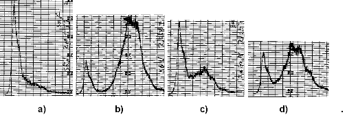
We then grew thinner (quantum) wells with growth times varying from 0.75 to 1.5 minutes (nominal thicknesses of 2 to 5 nm) and GaN barriers (50 nm above the well and ∼ 2 μm beneath it). Figure 5 shows the room temperature PL spectra for the four QW thicknesses. For the thinnest well, the PL spectrum is dominated by the GaN signal, and only shows a small shoulder on the low energy side. The next thickest well spectrum shows a peak, centered at 425 nm, but is broad with a FWHM of 200 meV. The height of this peak compared to the GaN peak varied widely across the wafer, and was typically much smaller than the example shown. The two thicker wells showed more consistent PL spectra shifted to higher energies, with the best overall quality occuring for the thickest (1.5 minutes). This would suggest that the nominal 5 nm well has the best quality and the largest quantum shift. The X-ray rocking curves for these four samples are shown in Figure 6. We see a dominant GaN peak with a small shoulder that is not due to the InGaN (which is too thin to give a significant X-ray response), but probably indicates strain in the 50 nm GaN capping layer due to the InGaN beneath it. This shoulder is largest for the thinnest well, and is much smaller for the thicker wells. We interpret this, combined with the evidence from the PL spectra, to mean that the thinnest wells are probably varying in thickness and may even be discontinuous. All wells are expected to have diffuse upper interfaces, due to the loss of In during the time while the wafer is heated back up to the GaN growth temperature. The wafers are presently being examined by TEM to verify this and to quantify the magnitude of the diffusion, but preliminary results suggest a diffuse interface rather than discontinuous layers.
Room temperature PL spectra for thin QWs with growth times of a) 0.75, b) 1.0, c) 1.25, and d) 1.5 minutes.
DCXRD plots for the four QW structures shown in Figure 5.

In order to evaluate the uniformity of the InGaN, a wafer with a 50 nm layer was mapped on a Waterloo PL mapper using a 325 nm He-Cd laser for excitation. Figure 7 shows the map and the histogram of the peak wavelength for the 50 mm wafer with a 2 mm edge exclusion. The average wavelength was 417 nm with a standard distribution of 8 nm. The actual variation is less than this since the mapper picks the highest peak, and the PL spectrum is modulated by the interference fringes caused by the large refractive index difference between the GaN and the sapphire substrate (the fringe spacing corresponds well with the measured total thickness of 1.5 microns).
PL map for a 50 nm InxGa1−xN layer (x = 0.18) grown on GaN. The standard deviation shown is increased by the presence of interference fringes in each individual PL spectrum, since the mapper software picks the highest peak as the peak wavelength.

A SQW LED was fabricated from material with the structure shown in Figure 8. Here we have added a 0.5 micron p-type GaN cap over the nominal 5 nm QW. Contacts were Ti/Al to the n side and Ni/Au to the p side. The Mg doping in this film was not properly activated and it had a relatively high resistivity, resulting in the high Vf of 16 V at 30 mA forward current. Figure 8 shows the EL spectrum from this diode, emitting at a peak wavelength of 473 nm, considerably longer than for GaN p-n junction LEDs, which typically emit at 420 nm. The broadness of this peak is probably due to the diffusion of the QW interface. The interference fringes observed here are closer together than those seen in the PL for the structure of Figure 7 since the total thickness of the III-N layers is 4.5 microns for this sample.
EL spectrum for a SQW LED with the structure shown in the inset. The operating current was 30 mA.

4. SUMMARY
The growth of InGaN quantum wells by MOCVD is described. These QWs were characterized by XRD and PL, and quantum confinement effects were seen. The experiments also showed that the QW interfaces were diffuse, due probably to In diffusion during the temperature ramp to the upper confining layer of GaN or AlGaN. A single QW LED was fabricated which emitted at a wavelength of 473 nm.


