

1 Introduction
Development of solid state lighting by means of light emitting diodes (LEDs) Reference Holonyak[1] Reference Akasaki, Wetzel, Shur, Mishra, Gil and Kishino[2] Reference Nakamura and Fasol[3] is an opportunity to lower the primary energy consumption significantly worldwide [4] [5] [6]. In the United States of America about 20% of all primary energy sources are being consumed for the purpose of lighting. Under realistic projections of the development and commercialization potential of high brightness semiconductor LEDs, as much as 28% of that amount can be saved. This amounts to the equivalent of 222 million barrels of crude oil every year. By 2002, research, development, and commercialization of high brightness LEDs has led to a 1.82 Billion-$/year world market Reference Steele[7]. This is about the volume of the US retail market sales for scented candles [8]. Market projections, however, foresee an averaged annual growth of the order of 20% for high brightness LEDs quickly outpacing the more traditional lighting market Reference Bergh, Craford, Duggal and Haitz[9].
The potential and projected energy savings rely on the concept of generating visible light without the heat that comes with the use of conventional incandescent lighting. A simulation of the solar spectrum in the visible range requires a light source to emit a spectral continuum from 400 nm to 680 nm. The human eye distinguishes only red, green, and blue colors in photopic vision (the actual maximum of sensitivity of the respective cone cells in the human eye are at 560, 530,and 420 nm, respectively Reference Verrelli and Tishkoff[10]). It therefore should suffice for human vision to limit the generation of light to the three colors of red, green, and blue Reference Schubert[11]. According to color theory, the sensation of white light can be generated in different ways, e.g., by mixing of the three primary additive colors red, green, and blue, and by mixing of complimentary additive colors like primary blue and secondary yellow. The impression of any subject’s color, (i.e., subtractive red or subtractive green), however, is possible only when the object is illuminated by white light that contains the wavelengths corresponding to that color. For example, a red tomato will only appear red when it is being illuminated with light containing red light and green foliage will only appear green when it is being illuminated with green light. White composed of merely blue and yellow cannot render green or red subtractive object colors. Light that generates the impression of white is not sufficient. For a good color rendering of various colors it therefore is necessary to provide white light sources that comprise all three, i.e., red, green, and blue (RGB) light emitters.
The current technology of white LEDs typically employs a combination of UV LEDs that excite a mix of phosphors optimized for RGB emission Reference Baur, Schlotter and Schneider[12] Reference Schlotter, Baur, Hielscher, Kunzer, Obloh, Schmidt and Schneider[13]. Due to their common primary excitation in the UV, such systems are strongly limited in their power efficiency. The wavelength transformation of each UV photon to a maximum of one photon in the visible implies an energy loss that scales with the emission wavelength. The loss is particularly large for emission in the green and red spectral range. The energetically better way is to eliminate the optical transformation process of the phosphor and to employ RGB emitting LEDs directly in a white RGB module.
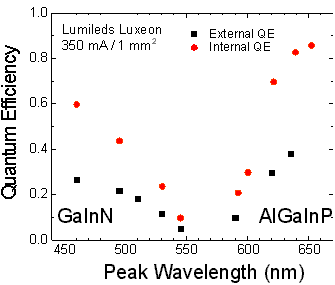
Stat of the art direct emitting RGB modules employ AlGaInP red LEDs at 670 nm, AlGaInN blue LEDs at 470 nm, and AlGaInN green LEDs at 525 nm. The current best performance of each subsystem characterized by the quantum efficiency is shown in Figure 1 adapted from Refs. Reference Goetz[14] Reference Krames[15]. The total quantum efficiency, i.e., the external quantum efficiency (EQE) is the product of internal quantum efficiency (IQE) and light extraction efficiency. The former describes the light generation efficiency and is primarily the result of epitaxial growth optimization and layer design. The latter is strongly controlled by die processing, contact metallization, and die shaping. From Figure 1 it is apparent that performance in the green (525 nm) and deep green (545 nm) spectral ranges is significantly lagging that of blue and red. Despite significant progress over the last decade, particularly by implementation of blue and UV AlGaInN group-III nitride LEDs, a substantial performance gap in the green and deep green spectral range forms a bottleneck for further technological and economic progress [4].
The current best performance of GaInN and AlGaInP systems characterized by the quantum efficiency (adapted from Ref. Reference Goetz[14] Reference Krames[15]). The low performance for the green, deep green, and yellow spectral region from 525 — 580 nm is apparent. Internal and external quantum efficiencies are being distinguished. The latter includes the light extraction probabilities and can be measured directly. Internal efficiency is typically extrapolated from the temperature dependence of the external one to zero Kelvin.
When addressing the internal quantum efficiency, a detailed understanding of the electronic bandstructure and the carrier recombination processes is of particular relevance. Both control the electron and hole injection properties, their confinement to the active region, their interband transition energies as well as their probabilities to recombine either radiatively or merely result in heating of the die. Over the recent years, we have developed a detailed understanding of the electronic bandstructure in GaInN/GaN thin films and quantum well (QW) heterostructures, the system that holds the highest promise for this spectral range from 495 – 560 nm Reference Wetzel, Takeuchi, Yamaguchi, Katoh, Amano and Akasaki[16] Reference Takeuchi, Wetzel, Yamaguchi, Sakai, Amano, Akasaki, Kaneko, Nakagawa, Yamaoka and Yamada[17] Reference Wetzel, Takeuchi, Amano and Akasaki[18] Reference Wetzel, Takeuchi, Amano and Akasaki[19] Reference Wetzel, Takeuchi, Amano and Akasaki[20] Reference Wetzel, Kamiyama, Amano and Akasaki[21]. We identified the unique role that huge piezoelectric and pyroelectric polarization plays in the optical absorption and light emission properties of such structures on a direct and quantitative basis Reference Wetzel, Takeuchi, Amano and Akasaki[18]. In particular, by combination of various optical spectroscopy techniques, we have directly quantified the polarization dipole strength acting across each QW and so laid a quantitative basis for bandstructure calculations and LED optimization Reference Wetzel, Takeuchi, Amano and Akasaki[19].
Using an interpolation of GaN and InN bandstructure parameters we determined all possible interband transition energies in effective mass perturbation theory. This allowed us to label and identify the transitions observed in emission and absorption-type spectra of 30 Å Ga1-xInxN/GaN QWs of variable InN-fraction x. A direct extrapolation of these results suggests that 525 nm green LEDs should be possible using active light emitting layers comprising 30 Å Ga1-x In x N (x = 0.20) QWs embedded in GaN barriers. We subsequently developed a 525 nm green LED production scale process using vertical flow metal organic vapor phase epitaxy (MOVPE) reactors Reference Wetzel, Salagaj, Detchprohm, Li and Nelson[22]. For un-encapsulated die we obtain a 525 nm dominant wavelength performance of 2 mW at 20 mA for a 2 inch wafer median and as high as 2.5 mW at 20 mA for individual die. Upon full packaging of these (400 μm)2 sized die, we expect a performance of 5 mW at 20 mA equivalent to 250 mcd of luminous flux. These values closely correspond to the best currently available by US companies, namely the Lumiled Luxeon II chip. Here we lay out details of the critical steps and achievements of this development.
This review is organized as follows: We first summarize our characterization results of multiple quantum well (MQW) material by means of optical spectroscopy to identify the proper device structure. We then present our green LED die implementation effort including epitaxy optimization, device development, and production yield optimization.
2 Bandstructure Spectroscopy
The analysis of the electronic bandstructure in GaInN/GaN has been the subject of some stimulating controversy. This in part has been spurred by discrepancies in the interpreted bandgap energies from absorption-type and emission-type experiments and by frequently observed lateral phase separation of GaInN alloy into In-rich and In-poor regions Reference El-Masry, Piner, Liu and Bedair[23] Reference Ponce, Cherns, Goetz and Kern[24] Reference Chichibu, Azuhata, Sota and Nakamura[25] Reference Smeeton, Kappers, Barnard, Vickers and Humphreys[26]. The reported length scale for such interpreted fluctuations varies by the characterization methods employed and ranges from ~25 nm Reference Zhou, Yu, Florescu, Ramer, Lee, Ting and Armour[27] to ~1μm Reference Wu, Elsass, Abare, Mack, Keller, Petroff, Den and Speck[28]. A proper assignment is ultimately difficult since GaInN/GaN sample material strongly varies with a wide range of growth parameters and growth processes.
In our approach, GaInN/GaN MQW sample material has been optimized for homogeneity of the crystal growth morphology as identified in x-ray diffraction and atomic force microscopy Reference Wetzel, Takeuchi, Amano and Akasaki[19]. Epilayers for this study have been grown by MOVPE in a horizontal flow reactor from TMGa, TMIn and NH3. A set of pseudomorphic Ga1-x In x N/GaN MQW structures with variable composition was grown on (0001) sapphire in c-plane growth using the technique of low-temperature deposited AlN buffer layers Reference Takeuchi, Sota, Katsuragawa, Komori, Takeuchi, Amano and Akasaki[29] Reference Takeuchi, Wetzel, Yamaguchi, Sakai, Amano, Akasaki, Kaneko, Nakagawa, Yamaoka and Yamada[17] Reference Wetzel, Takeuchi, Yamaguchi, Katoh, Amano and Akasaki[16]. On top of a 2 μm GaN epilayer five sequences of L w= 30 Å Ga1-x In x N QWs embedded in L b=60 Å GaN barriers were grown with x in the range of 0 ≤ x ≤ 0.2. For all samples, the well and barrier regions are nominally undoped at residual donor concentrations of about 1017 cm3. Excellent compositional homogeneity of the material on the length scale 1 < r < 50 μm was assessed by spatially resolved micro photoluminescence (PL) at excitation power densities of 1 mW/μm2 Reference Wetzel, Takeuchi, Amano and Akasaki[30] The full width at half maximum variation of the peak energy was typically < 20 meV. Photoreflection (PR) was measured using a Xe white light source and above-barrier band gap excitation at 325 nm by a 40 mW HeCd laser for photomodulation. A mechanical chopper at 1.4 kHz and lock-in technique was employed for the detection. To form the PR signal the ac component was normalized to the dc part. Due to the excitation geometry, thickness interference fringes did not occur in the ac part nor in the dc part Reference Wetzel, Takeuchi, Amano and Akasaki[18]. All experiments were performed at room temperature.
PL spectroscopy under both, high and low excitation power density has been performed on a series of samples with different InN-fraction as shown in Figure 2. Under low excitation density, broad spontaneous emission is observed in N 3. Stimulated emission in the range from 420 — 450 nm is seen under high excitation and labeled N 2. This emission occurs at substantially higher energies than the spontaneous one. The discrepancy can amount to 265 meV for x = 0.18 and exemplifies the great difficulties to develop longer wavelength laser diodes. In some works it was argued that there is a continuous transition from emission in the equivalent of N 3 to N 2 with increasing excitation density [31]. In our studies it appears as if both transitions were of different nature without a continuous connection. In a different experiment on the identical samples, PR spectroscopy was performed as shown also in Figure 2. Here the white light reflection was spectroscopically analyzed in sync with an on-off modulated above-bandgap photoexcitation by a 5 mW 325nm laser beam. This UV photoexcitation delivers photocarriers to the QWs and locally modulates acting internal electric fields. The resulting spectra are a partial field-derivative of the spectral reflectivity of the sample. As such it is very sensitive to the critical points in the joint density of states (DOS) of the QW structure. In contrast to the luminescence experiments, it does not emphasize any low-density-of-states trap and localization levels. In this low excitation power density experiment significant spectral features are observed near both levels, i.e., the low excitation density PL emission maximum near (N 3) and the stimulated emission maximum (N 2). At higher energies, additional levels are identified in N 0 and N 1. In N 1 a set of oscillations starts stretching out to higher energies. These have been identified as Franz-Keldysh oscillations (FKOs) in the presence of a large static electric field marking a three dimensional critical point in the joint DOS in N 1. N 0 is identified as the GaN interband transition between valence and conduction bands of the barriers. The oscillation period of the FKOs allows an accurate determination of the acting electric field strength F within the QW. The energetic splitting E(N 0) – E(N 1) = Fe L wis found to correspond to the polarization dipole across the well of width L w . The close correspondence of both quantities in a number of samples with different x and Lw provides an accurate measure of the actual electric field values within the individual structures and the corresponding polarization charges at the interfaces. It therefore forms a solid basis of detailed bandstructure calculations for such MQW systems.
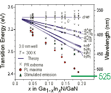
Spectroscopic analysis of Ga1-xInxN/GaN quantum wells optimized for lateral homogeneity with three different compositions and a fixed well width of 30 Å at room temperature. Photoluminescence (PL) under low and high excitation density are compared with photoreflection (PR) spectra. Observed transition levels are labeled N 0 to N 3. Bandstructure calculation results using the derived polarization field strengths are indicated and labeled by the subbands involved. An accurate reading of the electric field strength is possible by an analysis of the Franz-Keldysh oscillations above N 2. The polarization dipole F e L w produces the splitting between N 0 and N 1. The target of 525 nm green emission is indicated (after Ref. Reference Wetzel, Takeuchi, Amano and Akasaki[30]).

The experimental data points of low excitation density PL, stimulated emission, and PR are summarized in Figure 3. Included as full lines are the calculated interband transition energies under particular consideration of the selection rules in the presence of large electric fields. The bandstructure parameters employed in this calculation are primarily those of GaN. Where parameters of InN are known, linear interpolations have been used. The value of the bandgap energy of GaInN was taken directly from an interpretation of PR data in GaInN thin films Reference Wetzel, Takeuchi, Yamaguchi, Katoh, Amano and Akasaki[16]. The fact that the bandgap energy of InN has recently been reassessed at 0.67 eV has no implications on our experimentally determined bandgap values Reference Inushima, Mamutin, Vekshin, Ivanov, Sakon, Motokawa and Ohoya[32] Reference Davydov, Seisyan, Klochikhin, Ivanov, Emtsev, Bechstedt, Furthmüller, Harima, Mudryi, Aderhold, Semchinova and Graul[33] Reference Wu, Walukiewicz, Yu, Arger, Haller, Lu, Schaff, Saito and Nanishi[34] Reference Matsuoka, Okamoto, Nakao, Harima and Kurimoto[35]. For details of the calculation see Ref. Reference Wetzel, Takeuchi, Yamaguchi, Katoh, Amano and Akasaki[16].
Interpreted interband transition energies and theory results as a function of InN-fraction x in 30 Å Ga1-x In x N/GaN quantum wells. Maxima of the Franz-Keldysh oscillations are marked with thin line crosses. The low-excitation density PL maxima extrapolate to the target of 525 nm for x ≅ 0.20 in a 30 Å well (after Ref. Reference Wetzel, Takeuchi, Amano and Akasaki[30]).
At this stage, we have not identified the very nature of the PL emission transition itself. Our data suggests that it behaves like a low-energy sideband to the fundamental quantized transition e1hh1. The energy shift with respect to e 1 hh 1 is very close to the polarization dipole energy FeL w determined above from the splitting of N 0 and N 1. Detailed spectroscopic analysis is under way in many groups to identify the mechanisms leading to this Stokes-like shift. Among the most commonly cited alternative interpretations are alloy fluctuations of GaInN that could induce local potential minima that are too low in DOS to be observed in absorption-type experiments but efficient enough in photocarrier trapping to be emphasized in radiative recombination Reference Chichibu, Azuhata, Sata and Nakamura[36] Reference Nakamura and Fasol[3]. In another model, well thickness fluctuations are being considered Reference Zhou, Yu, Florescu, Ramer, Lee and Armour[37]. A further consideration is that polarization charge densities at the heterointerfaces vary strongly with growth parameters Reference Wetzel, Takeuchi, Amano and Akasaki[30] Reference Wetzel, Nitta, Takeuchi, Yamaguchi, Amano and Akasaki[38]. There seems to be supporting evidence for all those models and the large variety of different sample materials makes it difficult to unify the models at present. In our case, the clear PR signal suggests that no low-DOS processes are involved in the emission. The discrete energy levels also make it unlikely that they are part of a broadened energy distribution tail of any disorder effect. Instead, however, our model of polarization dipole induced levels seems to explain many aspects in our material at hand.
On the basis of this analysis it should be possible to develop 525 nm green emitting LEDs when using the emission of the low-excitation-density PL peak. An extrapolation of these results suggests a composition of the active layer of x = 0.20 and a well width of L w = 30 Å.
3 Optimization of Epitaxy
Our bandstructure characterization results formed the basis for the development of 525 nm green LEDs using Ga1-x In x N/GaN MQWs of the above identified geometry. Using MOVPE reactors with a vertical gas injection scheme and a 470 nm blue LED epi recipe as a starting point, we pursued several approaches to extent the emission wavelength into the green.
LED epi wafers have been grown by MOVPE in an Emcore D-180 Spectra GaN rotating disc multiwafer system using trimethyl and diethyl adducts of Ga, In, Al, as well as ammonia. Ga1-x In x N/GaN MQW structures in c-plane growth have been embedded in pn-diodes on 2-inch diameter (0 0 0 1) sapphire substrate Reference Wetzel, Salagaj, Detchprohm, Li and Nelson[22]. A low temperature deposited buffer layer initiated the growth of 3 μm GaN n-type doped with Si to N e = 3×1018 cm−3. Typical design parameters for the active region are as follows. Five Ga1-x In x N QWs of nominal well width L w = 3 nm, separated by barriers of nominal L b = 11 nm Reference Karlicek, Sakaki, Hirayama and Woo[39] have been grown at temperatures above 650° C. Resulting x-values are in the range of 0.15 to 0.20 as determined by x-ray diffraction analysis. There is no intentional doping in the active region and carrier injection layers are all nominally identical for electrons and holes, respectively. The p-side was formed by a 30 nm Al y Ga1-y N electron blocking layer (y ≅ 0.08) and 300 nm of GaN. Both layers were Mg doped to a nominal concentration of ~ 1019 cm−3. The resulting hole concentration was approximately 5×1017 cm−3in the p-type GaN layer. We made no use of methods such as lateral epitaxial overgrowth to reduce threading dislocation densities below typical values of ~ 109 cm−2. Samples are characterized at various stages of the process, i.e., prior to deposition of a p-side, the full pn-structure in epi form, and fully processed and separated bare die mounted on TO-18 header. None of our dies have been coated or specially shaped for any enhancement of light extraction. The final LED dies are (350 μm)2 or (400 μm)2 along the edges.
In several approaches we have used different optimization paradigms to obtain highest possible emission power in electroluminescence (EL) at the target wavelength of 525 nm. Overall a total of some 850 epi runs have been performed until a winning strategy has been identified leading to a highly stable production-worthy process. Within the LED development and manufacturing process, epitaxial wafers and dies were characterized at various stages in order to monitor material quality and development progress. Among the standard tools, PL was employed on the unprocessed epitaxial wafers, EL was performed on both, unprocessed and processed, wafers.
For the development of blue LEDs, PL emission, i.e., emission wavelength and emission intensity, are known to be good primary feedback parameters for growth optimization. One example of this optimization paradigm is the class of growth Condition A, which has led to the development of high performance 470 nm blue LED dies. Measured at the bare die, the light output from our dies reaches 3 mW at 20 mA drive current. In fully mounted and encapsulated form this performance typically doubles to 6 mW.
In other approaches, the primary focus was on the morphological homogeneity of the active layer, in particular in terms of the nanometer roughness of the growth surface. This was quantified by means of atomic force microscopy (AFM). Growth Condition B and Condition C are early and late stages of this paradigm, respectively.
A comparison of the growth Conditions A, B, and C in the terms of the growth morphology is shown in (Figure 4). Surface topography of the last barrier that covers the last of 5 GaInN/GaN QWs is shown in a surface height profile. No p-doped layers are present. Areas of 5 × 5 μm2 for conditions A, B, and C are shown using very different full scale height ranges of 50 nm (A), 10 nm (B), and 2 nm (C). Characteristic is the density and size of dark appearing pits. These have previously been identified as V-defects originating at the intersection of Ga1-x In x N layers and threading dislocations emanating in the underlying layers Reference Wu, Elsass, Abare, Mack, Keller, Petroff, Den and Speck[28]. Along the sequence of conditions, the density of pits decreases from 16 × 108 cm−2 (A), over 8 × 108 cm−2 (B), to 3.6 × 108 cm−2 (C), when counted using the image contrast of the given height scales. In parallel, the roughness decreases most notably from 15.4 nm root mean square (RMS) (A), over 0.96 nm (B) to 0.14 nm (C). The morphology in our high performing 470 nm blue LEDs is very similar to the data under Condition A. Apparently tremendous improvements in growth morphology over that of high performing blue emitting epi is possible within our optimization scheme.
Surface morphology after growth of the last barrier of the active region for three different classes of growth conditions in AFM. Note the different height scales. Density and size of V- defects and terrace curvature vary strongly (after Ref. Reference Wetzel, Salagaj, Detchprohm, Li and Nelson[22]).

The luminescence properties assessed by PL (T= 300 K, 325 nm excitation, P= 1.8 – 2.0 mW) of the same samples and locations (±5 mm) are given in Figure 5 (labeled MQW, no p-side present). All PL traces within the same panel use the same signal scale but different panels use different scales. Under Condition A, a broad emission band stretches from 500 — 700 nm with full width at half maximum (δ) of 120 nm. Fringes of layer thickness interference are found to be superimposed. Under Condition B, the spectrum is dominated by a strong blue line at 460 nm. In this case, green emission appears only as a low energy tail (δ = 70 nm). In Condition C finally, all emission occurs in the green, yellow, and red spectral range and with a rather large line width of δ = 130 nm. All of the described features are characteristic for these conditions while the exact wavelengths and intensities vary with common process parameters from epirun to epirun.
Photo- and electroluminescence in Ga1-xInxN/GaN active layers grown under three different classes of conditions. Green emission in the MQW of Condition B competes with strong blue emission. Linewidth for Conditions B and C is strongly reduced in the full LED structure over that in the bare MQWs. Electroluminescence closely follows the PL in Conditions B and C (after Ref. Reference Wetzel, Salagaj, Detchprohm, Li and Nelson[22]).

At this stage, it is not obvious which condition would be best for a 525 nm green LED die. The very broad line shape for all cases would likely raise big concern about the epitaxial quality of such wafers. It would be likely to attempt to optimize the growth process at this early stage of device fabrication for a much smaller luminescence line width such as 20 or 30 nm. In fact, the 470 nm blue LED process was developed in this way. For Condition B and Condition C, however, we refrained from such an approach and limited ourselves to the above mentioned optimization for morphological homogeneity as assessed by AFM.
Usefulness of any of the growth conditions for high power green LED dies, however, cannot be judged until these layers are implemented in full LED structures including highly doped n- and p-type layers. In the next step therefore, full LED epi wafers have been analyzed that embed active regions of growth condition A, B, and C inside a pn-junction.
The PL of the full LED structure is included in Figure 5 (labeled LED). Little variation in peak position and bandwidth with respect to the MQW data is observed under Condition A (peak near 570 nm, δ = 120 nm). This condition indicates properties that are rather insensitive to the presence of the p-side. In Condition B, the emission peak has shifted strongly towards the green at 520 nm at a constant δ = 70 nm. Here apparently the presence of the p-side plays an important role, and a LED performance conclusion based on data of the MQW alone would have been very misleading. In Condition C, however, we observe a strong narrowing of the emission band to δ =35 nm over that of the MQW. Again, optimization of the epitaxial growth to the PL of the MQW alone would have excluded our development of such a condition. The line narrowing after capping with a p-side can be explained by lateral charge transfer in the conducting n- and p-regions to compensate for spatial variations of the electrostatic and piezoelectric properties of the active region. Such a lateral compensation and equalization of the electrostatic potential is much less likely in the MQW samples where the piezoelectric highly charged active region is not capped by a conducting p-side. This is another manifestation of the strong electric fields controlling the electronic bandstructure and emission spectra.
All of the above considerations are meaningful only when they lead to a useful device which will be quantified in terms of EL performance. EL therefore is shown for the same samples of the full LED structure (labeled EL LED) (Figure 5). Under Condition A (peak at 503 nm, δ =32 nm), emission is significantly shifted to shorter wavelength versus the PL in bare MQW and LED. Despite the apparent insensitivity of PL to the presence of the p-side, electrical carrier injection in EL leads to entirely different results. Such an outcome is not surprising since the carrier injection mechanisms are entirely different in PL and EL. In photo excitation, carriers of both polarities are generated in the same location, while for electro-injection those carriers arrive from opposite sides of the wells Reference Wetzel, Takeuchi, Amano and Akasaki[40]. Electrons arrive from below the active region and flow along the polarized (0 0 0 1) direction, while holes flow opposite to this direction. Carriers consequently arrive from opposite sides to the asymmetric QWs which could be responsible for carrier thermalization and recombination processes that are different from those under same-side injection. In Condition B (peak at 515 nm, δ =34 nm) and Condition C (peak at 525 nm, δ =33 nm), however, the EL emission closely tracks the PL in the LED structure in peak and line width resulting in the desired EL emission near 520 nm.
The above findings give rise to our following interpretation. It has been established that threading dislocations penetrating the ternary well layer act as nucleation centers for V-defects Reference Wu, Elsass, Abare, Mack, Keller, Petroff, Den and Speck[28]. These defects are characterized by high index growth surfaces that offer enhanced In-incorporation efficiencies to an otherwise highly compressed InN-rich well layer. Similar to the well-documented case of enhanced Al-incorporation at high index growth surfaces in the growth of AlGaN Reference Kawashima, Iida, Miyake, Honshio, Kasugai, Imura, Iwaya, Kamiyama, Amano and Akasaki[41], growth of high InN fraction GaInN layers competes with effective In accumulation along such penetrating defects. This, on the one hand, may explain the great difficulty to shift the emission wavelength to longer wavelength into the green. On the other hand, it may explain the reduced light output, due to a reduced available area of (0 0 0 1) oriented alloy material and a possible increase in recombination shunt current through low energetic states within the In accumulation areas. It should be noted that in this interpretation the active green emission does not originate in the In accumulation areas but rather in the (0 0 0 1) oriented alloy layers that would tend to loose their In to such defects. The strong correlation of our die performance with surface roughness and pit density suggests that significant die performance improvements should become possible for MQW growth on GaN material that is free from threading dislocations.
Together these results provide a strong basis for the development of green LED dies. We here specifically find that Condition C, based on morphological and structural optimization of every component, provides the key for highest spectral performance in the desired green spectral range.
4 Wavelength-Power Behavior
Synonymous for the difficulty to develop high light emission power green LEDs is the observation of a strong decrease of the emission power when the emission wavelength is increased from the blue spectral range to the green Reference Goetz[14] Reference Krames[15]. This is well represented in the trends of Figure 1. The lacking performance of green emitters is apparent and particularly surprising since the same material system is employed for blue and the green. In order to assess the limits of the AlGaInN technology as a function of the emission wavelength, a large number of samples is required to compensate for fluctuations that are beyond the controllability of the epitaxial process. Natural run-to-run variations, be they intentionally controlled or uncontrollable process fluctuations, can easily cloud an analysis where statistical methods were more appropriate. In this approach, we analyzed the data of hundreds of growth runs during different development stages of the green LED epi production process. Relative epi performance can be determined on unprocessed LED epi wafers by applying a constant current of 100 mA through standardized In-contacts. In this step the spectral emission and integral emission power are analyzed. Performance data of LED epi manufactured on a single reactor over the time frame of several months and development stages are shown in the three panels of Figure 6 Reference Wetzel, Detchprohm, Li and Nelson[42]. Data of typically one wafer per growth run is being presented in this way. Data subgroups originating from the same location on different wafers are being shown in the same symbol color.
Relative emission power of unprocessed epi wafer as a function of wavelength for different growth optimization series over the time frame of one year. Within each series characteristic power-wavelength roll-offs are identified by straight lines that guide the eye. Percentages give the power drop at 480 nm versus 460 nm and 550 nm versus 500 nm. From left to right the green range sees significant improvements, both, in absolute emission power and roll-off behavior (after Ref. Reference Wetzel, Detchprohm, Li and Nelson[42]).

In Series 1 primary focus was placed on blue epi wafers emitting in the 460 – 480 nm range and growth optimization was according to Condition A above. A rough line to guide the eyes can approximate the trend of emission power versus dominant wavelength as indicated in Figure 6. The slope of this line corresponds to an emission power Pe roll-off η;blue = 1 - Pe (480nm)/Pe (460nm) of η;blue = 47 % when the wavelength increases from 460 nm to 480 nm. In the green spectral range only sparse data is available in this dataset at very low power that does not allow a meaningful interpretation. Within a second series of epi-runs, Series 4, that corresponds to Condition B, performance roll-off in the same blue spectral range accounts for about η;blue = 33 %. For this set, sufficient data is available in the green to draw an equivalent line as guide for the eye. Its slope corresponds to a very large power roll-off η;green = 1 - Pe (550nm)/Pe (500nm) = 77 % between the wavelengths of 500 nm to 550 nm. Within a third series of epi-runs, Series 7, corresponding to Condition C, substantial progress has been observed as to the absolute emission power in the green spectral range. Within this data, a similar analysis of the guide to the eyes we observe a change of the roll-off from η;green = 61 % to a mere η;green = 33 % in a substantial fraction of the wafers.
A similar analysis of Lumileds Luxeon II lamp performance can be performed using their published data Reference Goetz[14] Reference Krames[15]. When extrapolating their trend to 550 nm, we obtain a wavelength-power roll-off of η;blue = 11 % for the blue and η;green = 85 % for the green according to our above definitions.
While our data does not reflect fully processed die performance but rather epi-level EL performance, it is a very strong indication for significant improvements towards high output power performance of green and deep green LED dies.
5 Wafer Yield
Most critical to the success of an LED production process is the question of yield, i.e., number ratio of useful die to total dies. While peak performances are an important measure for the physical capabilities of a device concept, it is not until reproducibility and wafer-scale homogeneity prove a process production viable. Preferably an entire epi wafer shall produce exactly identical devices in all aspects. Temperature variations, variable wafer bending and pre-reaction-prone growth chemistry in the group-III nitrides are known to complicate an optimization towards such a goal. Full wafer mapping of device performance therefore is relevant Reference Wetzel, Li, Detchprohm and Nelson[43].
The data presented here stems from fully processed but un-separated bare (350 μm)2 dies without coating optimized under growth Condition B and Condition C. Full wafer maps of the die performance at a forward current of 20 mA across two selected 2-inch wafers typical for Condition B and Condition C are presented in Figure 7 and Figure 8, respectively. The right-hand inset gives the distribution of die numbers along the respective bins. The median, 5 %-tile, 95 %-tile values, standard deviation, and bin definitions are listed for the forward voltage V f (a), the emission power P e (b), and the reverse voltage V r (c). For the dominant wavelength ë dom distribution in d), the bin definitions — each 2.5 nm wide — and their occupation fractions are given. Forward voltage, spectral emission, and emission power are measured simultaneously. In a subsequent measurement, a reverse current of 10 μA is applied and the resulting V r is measured as shown in (d). Reverse voltages under a small reverse current are faster to measure than leakage currents directly. This measurement aims to characterize reverse leakage of the pn-junction.
Full wafer map of (350 μm)2 LED die performance of a wafer grown under Condition B. a) Forward voltage at 20 mA, b) emitted power at 20 mA, c) reverse voltage at -10 μA, d) dominant wavelength at 20 mA. The insets show the respective die distribution within the wafer, list median and other statistical values. A wide power distribution with low median values and a very wide wavelength distribution are characteristic for such growth under Condition B.

Full wafer map of (350 μm)2 LED die performance of a wafer grown under Condition C. a) Forward voltage at 20 mA, b) emitted power at 20 mA, c) reverse voltage at -10 μA, d) dominant wavelength at 20 mA. The insets show the respective die distribution within the wafer, list median and other statistical values. A narrow power distribution at a rather high power of 1.8 mW – un-encapsulated – and a very narrow wavelength distribution are characteristic for growth under Condition C (see also Ref. Reference Wetzel, Li, Detchprohm and Nelson[43]).

Under Condition B we obtain a very broad distribution of emission wavelengths. The 80 % of die that lie closest to the median cover a spectral range as far as 508.6 – 533.5 nm (Figure 7, panel a)). Under Condition C, however, those 80 % lie within the very narrow spectral range from 517.9 – 523.5 nm (Figure 8, panel a)). Similar findings hold for the visible emitted power. Under Condition B we find a broad distribution from 0.5 – 1.2 mW (5 % - tile 0.52 mW, 95 %-tile 1.17 mW with a median of 0.93 mW) (Figure 7, panel b)). Only for Condition C we find a consistent high power emission all across the wafer within the bin of 1.6 – 2.0 mW (5 %-tile 1.64 mW, 95 %-tile 1.91 mW with a median of 1.82 mW) (Figure 8, panel b)). The forward voltage proves very homogeneous across the wafers with median values of 3.05 V (Condition B, Figure 7, panel a) and 3.25 V (Condition C, Figure 8, panel a). The source for the consistently higher values under Condition C has not yet been identified. The reverse voltage is very homogenous at a high level in both cases.
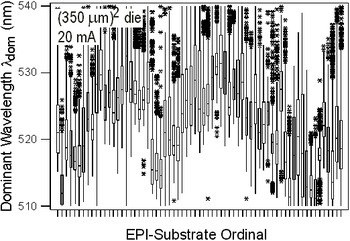
Relevance as a production process can be expressed by the longterm stability of the die performance from run to run and over extended periods of time. Typical die-relevant characterization parameters are summarized in Figure 9a, Figure 9b, Figure 9c, Figure 9d for the lower performing (350 μm)2 die as a function of ordinal number of produced wafer in a long period of consecutive epitaxial growth runs. We give the 846- point full wafer statistics in standard box-chart graphs. The values of upper and lower quartiles form a box around the median value. Upper and lower extrema are connected to the box by vertical lines. All statistical outliers are marked with crosses. Statistical data for dominant wavelength (Figure 9a), the emitted power in the visible range (Figure 9b), the forward voltage (Figure 9c), and the reverse voltages (Figure 9d) as evaluated in Figure 7 and Figure 8 are shown for 67 consecutively grown epi wafers under Condition C.
Wafer statistics of the dominant wavelength of 846 dies on 67 consecutively grown epi wafers under Condition C. Standard box-chart graphs with median, upper and lower quartiles, upper and lower extrema are shown. Statistical outliers are marked with crosses. A stable performance in the range of 515 – 530 nm is observed (see also Ref. Reference Wetzel, Li, Detchprohm and Nelson[43]).
The same wafer statistics as in Figure 9a is given for the emitted optical power. Power consistently ranges between 1.2 – 2.0 mW (see also Ref. Reference Wetzel, Li, Detchprohm and Nelson[43]).

The same wafer statistics as in Figure 9a is given for the forward voltage. Forward voltage is very stable around 3.2 – 3.4 V (Wafers with particular low variance have outliers lying very close so cross symbols overlap to bands) (see also Ref. Reference Wetzel, Li, Detchprohm and Nelson[43]).

The same wafer statistics as in Figure 9a is given for the reverse voltages.

We observe an excellent repeatability of all performance parameters and gradual improvement for emitted power and reverse voltage. Over this long range of wafer runs, a very high reproducibility of these key parameters is evident. The wavelength exhibits slow variations within the range of 515 – 530 nm while power increases almost continuously from run to run. In parallel, a reduced leakage under reverse bias is observed. This characterizes a gradual improvement and process stabilization during parts of a typical tool uptime cycle. In particular in light of the known Mg accumulation problems associated with this type of growth reactor and the employed growth chemistry emphasize the achievement of such stable performance in the green spectral range.
6 Green LED Performance
Using the so optimized epi-growth and fabrication optimization we developed green LED dies of different chip size: (350 μm)2 and (400 μm)2. Reference Wetzel, Salagaj, Detchprohm, Li and Nelson[22]. To this effect mesas were etched into the active layer. A semitransparent Ni/Au contact current spreading layer was deposited on the p-layer, n-and p-contact layers were formed, and the mesa was protected by a SiO2 layer. The sapphire substrate was thinned and dies were separated, mounted, and bonded on a heat sink with the epi side up. An encapsulation for index matching and packing was not performed. The following data is given for the (350 μm)2 die. Data for the (400 μm)2 die is given in brackets. The spectral emission as a function of forward current I f is shown in Reference Takeuchi, Wetzel, Yamaguchi, Sakai, Amano, Akasaki, Kaneko, Nakagawa, Yamaoka and Yamada[17]. Light output power versus I f is shown in Figure 10a (Figure 11a). Within a current range from 5 — 30 mA we observe a total variation of the dominant wavelength of 11 nm (11 nm). This is mostly attributed to a compensation of the quantum confined Stark effect in the presence of the internal piezoelectric field by the externally applied bias voltage Reference Takeuchi, Sota, Katsuragawa, Komori, Takeuchi, Amano and Akasaki[44] Reference Takeuchi, Wetzel, Yamaguchi, Sakai, Amano, Akasaki, Kaneko, Nakagawa, Yamaoka and Yamada[17]. Light output power versus I f is shown in Figure 10b (Figure 11b) together with the external quantum efficiency (EQE), and the resulting forward voltage. Power output also in our devices shows the sublinear behavior that is typically found in other blue and green GaInN/GaN LEDs Reference Goetz[14] Reference Krames[15]. This is reflected in a decreasing external quantum efficiency for higher current with a pronounced maximum at very low currents. For low-power applications, LED die operation at I f = 5 mA is typical. The present un-encapsulated design there delivers a radiant flux of 0.80 mW (0.54 mW) at Vf = 2.9 V (2.9 V), which is well within the capacity of cellular phone batteries. Traditionally, LED performance is quoted at I f= 20mA. At such a current we find Vf = 3.2 V (3.4 V) and a radiant flux of 1.6 mW (2.5 mW). The peak wavelength is 521 nm (523 nm) at a full line width at half maximum of 34 nm (32 nm), and the dominant wavelength is 523 nm (526 nm). The limited external quantum efficiency of about 3.4 % (5.3 %) reveals the strong potential for further improvements currently underway.
Summary of performance for the (350 μm)2 LED die. The spectral emission as a function of forward current revealing a blue shift of 11 nm of the dominant wavelength between 5 – 30 mA.

Summary of performance for the (350 μm)2 LED die. Emitted power, external quantum efficiency and voltage drop as a function of applied forward current.

Summary of performance for the (400 μm)2 LED die. The Spectral emission as a function of function of forward current (after Ref. Reference Wetzel, Salagaj, Detchprohm, Li and Nelson[22]).

Summary of performance for the (400 μm)2 LED die. Emitted power, external quantum efficiency and voltage drop as a function of applied forward current. The quantum efficiency reaches values of 7.5 % near 2 mA in this un- encapsulated device (after Ref. Reference Wetzel, Salagaj, Detchprohm, Li and Nelson[22])

In our approach, no effort has yet been paid to optimize the light extraction by means of any die shaping or epi roughening. Such processes are known to produce significant extraction gains Reference Schubert[11] Reference Kasugai, Miyake, Honshio, Kawashima, Iida, Iwaya, Kamiyama, Amano, Akasaki, Kinoshita and Shiomi[45]. Furthermore, all data was obtained on bare, i.e., un-encapsulated, die. For standard packaging and encapsulation with index matched layers and polymers we typically obtain a performance enhancement by a factor of 2.0. This or higher values are commonly observed throughout the industry when sapphire substrate based material in epi-up geometry is being packaged. Therefore, after full encapsulation we expect these dies to deliver a radiant flux of 3.2 mW (5.0 mW) at 20 mA and a luminosity of 130—160 mcd (200—250 mcd) based on experience with blue die material.
A typical device operation point of 20 mA was useful in LEDs for indicator applications. For lighting purposes, however, light output per production cost and/or operation cost is crucial. Therefore optimization aims at highest possible conversion efficiencies and current densities, i.e., highest light output from the smallest epi area. For this reason, devices for lighting applications are typically operated at current levels of 100 mA for a (350 μm)2 device or above.
A comparison of the die performance with Lumileds Luxeon II lamps Reference Goetz[14] Reference Krames[15] is possible when EQE is shown as a function of the drive current density. Under the assumption of the junction area of the Luxeon II (1 mm)2 and a typical light extraction enhancement factor of 2.0 for proper die encapsulation of our die, we obtain the data in Figure 12. It is apparent that our material reaches 95% of the performance of the Lumileds Luxeon II reference. In addition, it should be noted that the Luxeon lamp uses flip-chip technology while our dies use standard transparent p-contacts. This typically gives the Luxeon device a 25 – 40% advantage in light extraction. An extrapolation of our data under such an assumption is included in Figure 12 as a hatched band. This comparison suggests that epi material grown with our processes at the present stage can surpass the Luxeon II reference when processed and packaged in a similar way. Our material and processes therefore perfectly qualify for relevant and meaningful development and analysis. In particular, these results also lend relevance to the scientific exploitation of sample material obtained under the here described conditions.
Comparison of growth Condition C die performance with a commercial reference in terms of external quantum efficiency versus geometric current density. Published data for the flip-chip mounted Lumileds Luxeon II lamps is reproduced (black). Data for both dies sizes in this work (green, red) have been scaled by 2.0 for typical encapsulation gains in epi-up configuration. Additional extrapolation of the (400 μm)2 die data for typical gains by flip-chip mounting yields the hatched blue band which surpasses the commercial reference.

The strong improvements in die performance leading to bare green die powers of 2 mW and above are accompanied by a significant variation of the power roll-off behavior with wavelength. This lends support to the idea that the roll-off is not an inherent limit to the system but instead can be controlled on a rather high performance level by material and device optimization.
7 Future work
Our analysis also provides a direction for further device performance improvement. Figure 13 summarizes the discussed values of observed roughness of the active layer together with emission power and power roll-off fraction in the green spectral range as a function of the counted V-defect density for growth conditions A, B, and C. Indicated also are rough linear extrapolations on the presented scales as hatched bands. Under the assumption of a causal correlation of the data as suggested in these clear trend lines we should expect zero power roll-off for a vanishing V-defect density, i.e., < 108 cm−2. Under such conditions, the roughness should be of the order of 0.01 nm RMS, which is not so likely to be achieved experimentally. The emitted power of (350 μm)2 devices should scale from 1.6 mW to 2.0 – 2.5 mW at 20 mA without any other modification to the structure. Inversely, an extrapolation to zero emission power allows an estimate of the emission-dead area of the V-defect. For a V-defect density of 2.5×109 cm−2 we expect that no regular emitting area is left corresponding to a diameter of emission-dead area associated with individual V-defects of 220 nm. This is in reasonable agreement with the V-defect sizes observed in the AFM data of Figure 4.
Comparison of characteristic quantities versus the observed V-defect density under growth Conditions A, B, and C. The AFM roughness increases with the V-defect density (blue triangles, right y-axis). In extrapolation the roughness should fall to values of 0.02 nm RMS for vanishing V-defect density. The magnitude of the power roll-off in the green spectral range (500 – 550 nm) dies decreases with decreasing V-defect density (green circles, far left y-axis). The roll off should disappear altogether for vanishing V-defect density. The power of un-encapsulated (350μm)2 increases with decreasing V-defect density and should reach values of 2.5 mW for vanishing V-defect density, i.e., below 108 cm−1 (red squares, left y-axis).

We consequently see two possibilities to improve green LED die performance on the epi level. The first would be approaches to further reduce the V-defect decoration of existing threading dislocations. The second would be to avoid threading dislocations altogether, i.e., by means of advanced lateral overgrowth techniques or by use of single crystalline bulk substrates. The latter approach also bears the potential to increase the performance beyond our 2.5 mW extrapolation.
8 Conclusion
On the basis of detailed electronic bandstructure analysis results, we have devised and laid out an epitaxy optimization scheme that results in high light output power performance of 525 nm green LED dies. This process optimization goal is substantially different from that of 470 nm blue LED dies. We find that optimization to epitaxial homogeneity of the active region is relevant to the achievement of a high yield, uniform performance, and highly reproducible epitaxy process or green LED dies. We presented all respective performance parameters and extrapolate to future device performance upon the likely further reduction of structural defects. Our materials and processes resulting in die performance equivalent or better than industrial reference points proves a relevant platform for meaningful device characterization and further performance development along the goals of Solid State Lighting and energy conservation.
Acknowledgments
The authors gratefully appreciate the technical support and dedicated effort of all employees of Uniroyal Optoelectronics, Tampa, FL, in the early phase of this work, in particular Dr. D.C. Miller, Dr. J.S. Nelson, Dr. M.H. Crawford, Dr. C.J. Eiting, Dr. W.V. Schoenfeld, Dr. P. Li, and Mr. T. Salagaj.


