

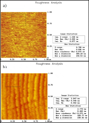
 0) of these structures was 0.099 nm.
Introduction
Recent topics of focused research in the III-Nitride community have been the selective area growth coupled with lateral epitaxial overgrowth (LEO) and the application of this tandem process route to reduce the dislocation density of GaN films by several orders of magnitude in the overgrown areas. A new form of selective and lateral growth, namely ‘pendeo (from the Latin: to hang or be suspended ) -epitaxy’ has been recently pioneered in our groupReference Linthicum, Gehrke, Thomson, Tracy, Carlson, Smith, Zheleva and Davis 1 - Reference Zheleva, Thomson, Gehrke, Linthicum, Rajagopal, Smith and Davis 3 , to achieve large area growth of III-N films having a continuous low dislocation density over the entire surface. This process route is based on the growth of GaN off a side wall and the ability to laterally overgrow a mask that has been employed to stop vertical propagation of line and planar defects. Additional details of this procedure and the initial results of this research have been reported previouslyReference Linthicum, Gehrke, Thomson, Carlson, Rajagopal, Smith and Davis 4 , Reference Zheleva, Thomson, Linthicum, Smith and Davis 5 .
In this paper we report the growth via pendeo-epitaxy of layered thin film structures consisting of GaN and AlxGa1−xN. The following sections describe the experimental procedure necessary to achieve layered structures by this technique in detail and discuss the results and conclusion of this study.
Experimental Procedure
Layered structures containing GaN and AlxGa1−xN have been grown on a 0.5 μm to 1.0 μm thick GaN seed layer grown on a high temperature, 100 nm thick AlN buffer layer previously deposited on a 6H-SiC(0001) substrate. All layers were grown using a cold-wall, vertical pancake style, RF-inductively heated metalorganic vapor phase epitaxy (MOVPE) system. The AlN buffer layers and the hexagonal GaN seed layers were each grown within the susceptor temperature ranges of 1080°C-1120°C and 980°C-1020°C, respectively, at a total pressure of 45 Torr. Triethylaluminum (20-25 μmol/min), triethylgallium (23-29 μmol/min), and NH3 (1.5 slm) precursors were used in combination with a H2 (3 slm) diluent. A 100 nm thick silicon nitride layer, employed as a growth mask for blocking the continued threading dislocations during the pendeo-epitaxial growth stage, was deposited using a plasma enhanced chemical vapor deposition (PECVD) system. A 150 nm layer of nickel was subsequently deposited as an etch mask and patterned in 〈
A JEOL 6400 FE scanning electron microscope (SEM) and an Digital Instruments, Inc. Dimension 3000 atomic force microscope (AFM) operating in the tappingMode™ with an Olympus tapping mode etched silicon probe were employed for microstructural characterization.
Result and Discussion
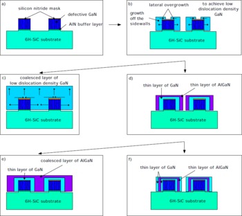
Figure 1 shows a schematic flow diagram of the process route for achieving pendeo-epitaxial growth of continuous layers of (c) GaN or (e) AlxGa1−xN. The intermediate steps in this approach can also be used to achieve the growth of (d) a double layer heterostructure of GaN and AlxGa1−xN, and a subsequent growth of (e) a continuous coalesced layer of AlxGa1-xN or (f) a layered double heterostructure of GaN/ AlxGa1−xN /GaN.
Schematic flow diagram showing the steps from (a) the etched columnar forms in the GaN seed layers to (b) lateral growth off the side walls of the seed layer and lateral overgrowth over the silicon nitride mask, to the growth of either (c) a continuous coalesced GaN film, or (d) a discrete bi-layer of GaN and AlxGa1−xN from which further growth results in either (e) a continuous coalesced layer of AlxGa1−xN or (f) a multi-layered structure of GaN and AlxGa1−xN layers.
Each of the microstructures depicted in Figure 1 has been realized in this research, as shown in Figure 2. The scanning electron micrographs in the latter figure illustrate (a) the 〈
Scanning electron micrographs of (a) etched columnar forms in a GaN seed layer, (b) lateral and vertical growth phenomena during pendeo-epitaxy, (c) a continuous coalesced layer of GaN, (d) a discrete bi-layer structure of GaN and Al10Ga90N, (e) a continuous coalesced layer of Al10Ga90N, and (f) a multilayered structure of GaN/Al10Ga90N/GaN.
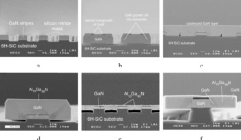
The GaN layer shown in Figure 2(d) was grown for 35 min at a susceptor temperature of 1075°C and for 2min at a susceptor temperature of 1090°C. The additional layer of Al10Ga90N was grown for 20 min at1090°C. This alloy layer appears in the scanning electron micrographs as a slightly darker cap atop the GaN layer. To produce the heterostructure shown in Figure 2(e) a thin GaN layer was grown for 2 min at a susceptor temperature of 1070°C and for 2 min at 1090°C. The Al10Ga90N was deposited using three growth steps at the susceptor temperatures and times of 1090°C and 2 min, 1110°C and 50 min, and 1090°C and 30 min. The second step was employed to force the Al10Ga90N to grow laterally and coalesce; the third step was used to grow the film vertically. The growth rate of Al10Ga90N films was markedly lower at both 1090°C and 1110°C than that of the GaN at any temperature employed in this study. A multi-layered structure shown in Figure 2(f) was also realized using several different growth parameter.
The first layer of GaN was grown at susceptor temperatures of 1075°C for 3 min and 1090°C for 2 min. The subsequent layer of Al10Ga90N was grown using susceptor temperatures of 1090°C for 10 min and 1075°C for 5 min. The temperature during the Al10Ga90N growth was not increased to 1110°C to limit the lateral growth. The additional layer of GaN was grown at a susceptor temperature of 1075°C for 10 min. The scanning electron micrograph in Figure 2(f) shows 60°interface planes between each layer. During the GaN growth the angled planes were growing out to the (00
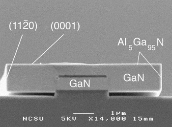
The bi-layer structure in Figure 3 consists of a GaN layer grown at susceptor temperatures of 1075°C for 35 min and 1090°C for 2min and a capping layer of Al5Ga95N grown for 20 min at a susceptor temperature of 1090°C. This structure possessed extremely smooth (0001) top and(11
Scanning electron micrograph of a bi-layer structure of GaN and Al5Ga95N used for AFM measurements.
Atomic force micrographs of a)the surface of the side walls represented by the (1120) plane, b) the top surface of the structure represented by the (0001)
Conclusion
Pendeo-epitaxial growth of layered structures of GaN and AlxGa1−xN has been achieved. The process steps for growing continuous coalesced GaN and AlxGa1−xN layers have been discussed in detail. According to this steps the process routes for growing layered structures of GaN and AlxGa1−xN have been introduced and discussed. The top surface and side walls of this structures have been characterized by atomic force microscopy and a RMS roughness of 0.548 nm and 0.099 nm, respectively, has been reported.
Acknowledgments
The authors express their appreciation to Cree Research, Inc. for supplying the SiC wafers. This work was supported by the Office of Naval Research under the contract # N00014-96-1-0765, N00014-98-1-0384 with C. Wood as technical monitor, and N00014-98-1-0654 with J. Zolper as technical monitor.


