Introduction
(0001)-oriented sapphire is the main substrate used for the realization of GaN-based devices [Reference Nakamura, Senoh, Nagahama, Isawa, Yamada, Matsushita, Kiyoku and Sugimoto1]. To our knowledge, very few reports deal with MOVPE of GaN on slightly misoriented sapphire [Reference Hiramatsu, Amano, Asaki, Kato, Koide and Manabe2-Reference Pecz, di Forte-Poisson, Huet, Radnoczi, Toh, Papaioannou and Stoemenos4], and only one concerns HVPE on such substrates [Reference Seifert, Fitzl and Butter5]. However, for other III/V compounds GaAs or InP, it has been shown that the use of substrates misoriented by a few degrees can be very efficient to improve both crystal quality and surface morphology of the layers grown by HVPE. This is related to the fact that the supersaturation of the gas phase is quite small in the hydride technique as opposed to the conditions during MOVPE growth and growth occurs near the thermodynamic equilibrium as predicted by the Burton, Cabrera, and Frank theory [Reference Burton, Cabrera and Frank6].
Experimental Details
Growth experiments have been carried out in two separate reactors. An horizontal home made reactor was used to grow low temperature GaN buffer layers prior to the growth by HVPE. Nitrogen and gallium precursors were ammonia (NH3) and trimethylgallium (TMG) respectively and carrier gas was nitrogen.
Deposition temperature was 600°C after a nitridation step of the Al2O3 surface at 1100°C during 30 minutes. All the experiments were carried out at atmospheric pressure.
HVPE layers were subsequently grown in an horizontal Aixtron HVPE reactor. Details on the reactor geometry have been published in a previous paper [Reference Parillaud, Wagner, Bühlmann and Ilegems7]. GaCl resulting from the reaction of HCl with metallic gallium and NH3 are brought separately to the deposition zone. Nitrogen and mixed nitrogen / hydrogen were used as carrier gas. Source temperature and deposition temperature were kept constant at 900°C and 1050°C respectively for all the experiments presented here. All the samples were non intentionally doped.
Substrates used were exact C-axis oriented sapphire and C-axis with 2°, 4° and 6° misorientation towards M and A axis.
Results
Low temperature MOVPE buffer layers.
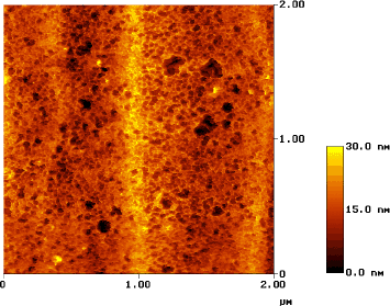
Some authors have proposed a GaCl pre-treatment of the sapphire surface [Reference Naniwae, Itoh, Amano, Itoh, Hiramatsu and Agasaki8] or a sputtered ZnO intermediate layer [Reference Detchprohm, Hiramatsu, Itoh and Agasaki9,Reference Molnar, Nichols, Malki, Brown and Melngailis10] to facilitate the initial stage of nucleation of GaN. In our case, we use a thin (10nm) GaN buffer layer deposited by MOVPE at low temperature [Reference Wagner, Parillaud, Bühlmann and Ilegems11]. These layers have been characterized by X-Ray diffraction before and after annealing up to 1050°C in the HVPE reactor. This annealing was carried out under NH3 atmosphere in order to prevent GaN decomposition. The Ω-rocking curves of the (002) GaN reflection after annealing develop into a broad peak which indicates that ordering of the small GaN grains is taking place. Atomic Force Microscopy was also performed on both exact and misoriented samples. The AFM picture presented in figure 1 clearly shows the grain structure of the buffer layer deposited on a 2° towards A oriented substrate before annealing. Pictures taken after annealing are similar and no clear evidence of a morphological change could be detected whatever the misorientation of the samples. A 30 nm high macro-step originating from the substrate surface is visible in the middle of the picture indicating that the final polishing of the sapphire surface does not lead to atomic steps.
AFM picture of the GaN buffer layer surface before annealing. Small GaN grain structure is clearly visible and a 10 nm high macro-step can be observed in the center of the image.

HVPE layers
3 sets of experiments are presented here. The growth conditions, the samples used, the layer thickness and FWHM of XRD Ω-scan are listed in table I. The growth duration was 15 min. for all runs. Set #1 corresponds to the growth conditions usually used on exact sapphire. Sets #2 and #3 have been carried out under different vapor phase composition. H2 was introduced in carrier gas for set #2 and the V/III ratio was divided by a factor of 10 for set #3. Thickness was measured by cross-section optical microscopy after cleaving. Top view optical microscopy, Scanning Electron Microscopy (SEM) and AFM were used to check the surface morphology and evaluate the roughness.
Growth conditions, substrates used, thickness and FWHM of XRD Ω-scan measured for the 3 different sets of experiments.

Figure 2 shows optical micrographs of the samples listed in table I. Only layers grown on exact (0001) and 2° misoriented substrates are shown, as the surface morphology obtained on 4° and 6° misorientated substrates was increasingly degraded. Layers grown on exact sapphire exhibit typical hillocks and pyramids, depending on growth conditions. Cracks are also visible for all the exact samples. On misoriented substrates, a directed step-flow growth mode is dominant with steps perpendicular to the direction of misorientation. However, the expected smoothening of the surface does not occur due to large step bunching effects which lead to more or less parallel steps or a fish scale appearance. The introduction of hydrogen as part of the carrier gas (set #2) improves the surface morphology and can be a key issue for the use of misoriented substrates, since the surface diffusion is enhanced. All the misoriented samples exhibit hexagonal pits whose density increases dramatically for set #3.
Optical microscopy views of the surface of 9 samples listed in table I. For each set of experiment, exact, 2° towards M and 2°towards A are presented.

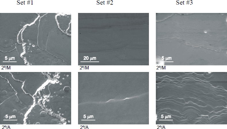
The SEM pictures of the misoriented samples are presented in figure 3. In case of set #1, a high density of small hexagonal pits is observed along the step edges. It is not yet clear if the pits are the cause of or are caused by the macro-steps. Furthermore, we find that the crack density is greatly reduced in the direction parallel to the steps. AFM studies (figure 4) bring additional information on the surface roughness between the macro-steps and on the formation of these macro-steps. Typical atomic steps are detected between macro-steps. The macro-step height varies from 10 nm for set #1 and #2 to more than 100 nm for set #3. All layers exhibit a high density of dark spots, typically less than 1 μm in diameter, which are indicative of emerging dislocations. These dislocations tend to block the advance of the atomic steps and partly explain the formation of the macro-steps.
SEM pictures of the 2° misoriented samples (top: towards M, bottom: towards A)

AFM pictures of the 2° misoriented samples (top: towards M, bottom: towards A, set #1 and #2 10×10 μm2, vertical scale 10 nm; set #3 40×40 μm2, 400 nm)

XRD measurements have been performed on all the samples. The FWHM of the Ω-rocking curve of the GaN 002 reflection is listed in table I. No clear improvement of the crystal quality can be deduced from these values. For the range of conditions explored, the samples misoriented towards A axis exhibit the lower values while values measured for exact and misoriented towards M samples are in the same range.
Discussion and Conclusion
As expected, the growth is affected by the misorientation of the substrates and a step-flow growth mode is evident. However, major step bunching effects occur, even at low angles of misorientation and whatever the direction of the misorientation (A or M). Furthermore, the surface morphology degrades dramatically for substrates with 4° and 6° misorientation. The causes suspected for this step bunching are strain relaxation and the large number of misfit dislocations generated at the sapphire / GaN interface that propagate up to the surface and block the steps, as evident on the AFM pictures. The presence of macro-steps on the substrate surface before the growth can also enhance this behavior. A slight improvement of the FWHM of the X-Ray rocking curve is observed for samples grown on 2° towards A misoriented sapphire and under mixed N2/H2 carrier gas. Overall, the results of this work do not suggest that significant improvement in crystalline quality or surface morphology can be expected by growth on misoriented (0001) substrates.