Introduction
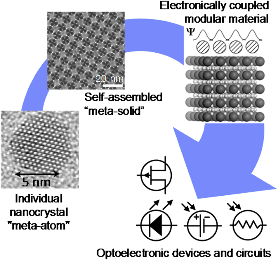
For the past century, the atom has been the building block of chemistry. Small atomic assemblies, aka molecules, remain the most fundamental and important concept in chemistry.Reference Pauling1 However, organized structures can form spontaneously, not only from atoms and small molecules, but also from various other types of building blocks. This process called “self-assembly” allows expanding and generalizing the concepts of bottom-up design and synthesis of structures, materials and devices. Self-assembly creates an opportunity to develop new paradigms for chemistry and material science, where various, typically nanometer-sized, objects with precisely engineered sizes, shapes, compositions, and concomitant properties serve as “meta-atoms” or superatomic building blocks for hierarchically assembled materials and devices. Just as atoms combine to form molecules with dramatically different properties than the atomic constituents, self-assembly of “meta-atoms” can create “meta-molecules,” and “meta-crystals.” Ultimately, self-assembly should contribute to the development and manufacturing of materials and devices for real-world applications (Figure 1). This issue of MRS Bulletin discusses examples of the successful adaption of self-assembly principles to the needs of electronics,Reference Kagan, Hyeon, Kim, Ruiz, Tung and Wong2 photonics,Reference Rainò, Utzat, Bawendi and Kovalenko3 energy storage,Reference Chen, Benedek, Fisher, Wood and Cui4 chemical separations,Reference Chen, Day and Zhou5 and complex structure formation.Reference Pashuck, Seeman and Macfarlane6 Self-assembly also plays a central role in biological systems and living organisms. These strong conceptual ties between self-assembly and biology open a wide design space for biomimetic materials.
Self-assembly enables the transition from precisely engineered nanoscale building blocks, or “meta-atoms,” to macroscopic functional materials used for devices and applications.

What is self-assembly good for?
Self-assembly adds several unique features to our existing toolset of chemical and physical methods for the synthesis and processing of functional materials. First, self-assembly allows making materials with structural features on the length scales of several nanometers, in not only two dimensions, but also in three dimensions, which is too large for traditional (atom-by-atom) chemical synthesis but too small to be efficiently approached by top-down techniques, such as photolithography (Figure 2a).
(a) Self-assembly allows organizing matter on length scales not achievable by traditional chemical synthesis and top-down nanofabrication techniques such as photolithography, imprint lithography, and even e-beam lithography. (b) The hierarchical nature of the materials synthesized by self-assembly: diblock copolymer chains (left panel) self-organize in the lamella stacks driven by the repulsive interactions between the polymer blocks (middle and right panels). The right panel shows an SEM image of a self-assembled diblock copolymer film. If desired, one of the blocks can be selectively dissolved and the obtained template can be used to fabricate semiconductor nanoelectronic circuits on a length scale difficult to achieve via traditional top-down photolithographic patterning. Right panel adapted with permission from Reference 8. © 2015 National Academy of Sciences.

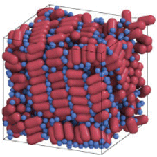
Self-assembly is particularly useful to synthesize hierarchically organized materials with structures independently engineered on different scales. For example, a variety of macromolecules containing two or more covalently bonded blocks of different polymers can be prepared by conventional chemical synthesis. These block copolymers spontaneously self-assemble into ordered structures with ~10 nm features (Figure 2b). The type of self-assembling structure and feature size can be rationally engineered by controlling the block size of individual molecules.Reference Mai and Eisenberg7,Reference Hur, Thapar, Ramírez-Hernández, Khaira, Segal-Peretz, Rincon-Delgadillo, Li, Müller, Nealey and de Pablo8 A similar hierarchical design is achieved for nanocrystal solids that can be engineered at the level of individual nanocrystals and then self-assembled into superlattices with the structure of glasses, crystalline solids, or quasicrystals (Figure 1).Reference Boles, Engel and Talapin9
Different approaches to classify self-assembly phenomena
Self-assembly is a unifying umbrella for a broad range of effects observed in different materials, and there are several excellent reviews discussing self-assembly on molecular, nano-, micro- and macroscopic length scales.Reference Mai and Eisenberg7,Reference Boles, Engel and Talapin9–Reference Love, Estroff, Kriebel, Nuzzo and Whitesides12 Self-assembly is observed in hard condensed-matter systems, such as epitaxial semiconductor quantum dots formed by strain-guided Stranski–Krastanov growthReference Galitsyn, Lyamkina, Moshchenko, Shamirzaev, Zhuravlev, Toropov and Bellucci13 and template-direct eutectics.Reference Kulkarni, Hanson, Zhang, Thornton and Braun14 There are many examples of self-assembled soft-matter systems, with block copolymersReference Mai and Eisenberg7,Reference Förster and Plantenberg11 and DNA origamiReference Hong, Zhang, Liu and Yan15,Reference Rothemund16 as well-known examples. Finally, hybrid systems incorporating hard and soft components, such as colloidally synthesized inorganic nanocrystals with organic capping ligands,Reference Boles, Engel and Talapin9,Reference Zherebetskyy, Scheele, Zhang, Bronstein, Thompson, Britt, Salmeron, Alivisatos and Wang17 combine the advantages of hard and soft components within the same material.
Given the breadth of self-assembly phenomena and materials systems, the classification of these effects can be approached from different angles. Thus, we distinguish equilibrium or static and nonequilibrium or dynamic self-assembly. In the former case, the ordered structures form when the system spontaneously evolves toward the global or local minimum of free energy. The organized structures represent equilibrium states and, once formed, remain stable. The assembly process is controlled by the free-energy landscape. This landscape can be modified (e.g., by applying external fields, temperature gradients, and other stimuli to drive assembly toward a particular outcome). These approaches often come under the name of “directed self-assembly.” In dynamic self-assembly, on the other hand, structures or patterns form away from equilibrium.Reference Grzybowski, Fitzner, Paczesny and Granick18 Such patterns require continuous energy input and disappear in the absence of an external drive. Nonlinear nonequilibrium oscillatory chemical reactions (e.g., the Belousov–Zhabotinsky reaction),Reference Vanag and Epstein19 are simple examples of nonequilibrium self-assembly. Biological systems represent much more complex networks of dynamic assembly.
Generally, self-assembly is associated with noncovalent interactions, such as van der Waals forces, long-ranged electrostatic, magnetic interactions, and hydrogen bonding.Reference Bishop, Wilmer, Soh and Grzybowski20 These “weak” forces are favorable for reversible interactions between macromolecular or particle building units, where reversibility is required for healing incorrect bonds and growing ordered domains.Reference Whitesides and Boncheva21 From the big-picture view, equilibrium self-assembly can be described using established theoretical frameworks of nucleation and growth.Reference Boles, Engel and Talapin9 However, when the assembling blocks are larger than atoms and small molecules, the interactions can be much more complex than interatomic forces. Moreover, the interactions can be rationally engineered in terms of magnitude, range, and specificity.
One can roughly define three categories of such interactions (Figure 3). In the first category, the local assembly rules are binary like-dislike type interactions (e.g., between hydrophobic and hydrophilic domains of a polymer backbone).Reference Förster and Plantenberg11 Even these simple interactions, combined with precise control over size and shape of assembling units, can lead to complex structures.
Classifications of interactions between building blocks utilized in self-assembly of functional materials.
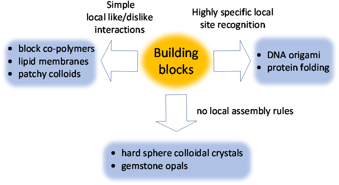
The next level of complexity and engineerability is achieved when the building blocks exhibit highly specific interactions with respect to each other. The best examples come from biology, with DNA being the most famous molecule capable of exchanging information via local intermolecular interactions. In humanmade materials, this concept laid the foundation for the field of DNA nanotechnology.Reference Seeman and Sleiman22 Highly specific site recognition has been implemented in metal–organic frameworks,Reference Furukawa, Cordova, O'Keeffe and Yaghi23 colloidal systems,Reference Macfarlane, Lee, Hill, Senesi, Seifert and Mirkin24,Reference Nykypanchuk, Maye, van der Lelie and Gang25 and is widely used in drug development.
Finally, complex ordered structures can form spontaneously even in the absence of any local attractive or repulsive forces between assembling units. This can be demonstrated using hard colloidal spheres that do not experience any interactions except bumping into each other. In a concentrated solution, these spheres spontaneously self-organize into long-range ordered domains.Reference Pusey and van Megen26 Counterintuitively, it is a system's entropy that organizes hard spheres into an face-centered-cubic (fcc) crystal.Reference Boles, Engel and Talapin9 Complex structures emerge when using nonspherical particles and when hard spheres of two different sizes are mixed together.Reference Bartlett, Ottewill and Pusey27,Reference Damasceno, Engel and Glotzer28
Theoretical and computational insights in self-assembly
Self-assembly processes of nanoscale building blocks are founded on statistical mechanics. Modeling is best accomplished with computer simulations. There are three closely related challenges: (1) handling a vast number of degrees of freedom, (2) accurate representation of microscopic interactions, and (3) following the evolution of the system for sufficiently long times. It is impossible to tackle all challenges at once, which is why a range of strategies have been developed, each with strengths and weaknesses and each at different level of spatial and temporal coarse-graining resolution (Figure 4).
Theoretical and computational modeling strategies for self-assembled functional materials at the nanoscale. (a) Oleic acid molecules on the PbS(111) surface. Adapted with permission from Reference 17. © 2014 AAAS. (b) Gold nanoparticles coated with 1-hexadecanethiol and dispersed in decane. Adapted with permission from Reference 38. © 2018 American Chemical Society. (c) Self-assembled AB2 binary spherocylinder-sphere superlattice. Adapted with permission from Reference 33. © 2013 American Chemical Society. (d) Free-energy density of the block polymer gyroid phase (Ia3̅d) computed with the self-consistent field method. A typical type of application, a main strength (+) and a main weakness (−) are listed for each. The level of coarse-graining (characteristic length and time scale, given at the bottom) increases from the left to the right. Adapted with permission from Reference 44. © 2016 American Chemical Society.

It is rarely necessary to include quantum mechanical effects explicitly in the modeling process to study self-assembly. But quantum effects can become relevant when analyzing physical and chemical properties of the final self-assembled material. Ab initio quantum chemistry methods can assist parametrization of coarser simulations with classical force fields, which foremost must reproduce van der Waals force accurately as those are often difficult to estimate and most crucial for self-assembly. All-atom simulations are best suited to resolve molecular processes where individual atoms are essential,Reference Weerawardene, Häkkinen and Aikens29 such as conformation changes,Reference Shaw, Maragakis, Lindorff-Larsen, Piana, Dror, Eastwood, Bank, Jumper, Salmon, Shah and Wriggers30 quantum dots,Reference Long and Prezhdo32 crystallization,Reference Loh, Sen, Bosman, Tan, Zhong, Nijhuis, Král, Matsudaira and Mirsaidov31 or at interfaces (Figure 4a).Reference Zherebetskyy, Scheele, Zhang, Bronstein, Thompson, Britt, Salmeron, Alivisatos and Wang17 The number of atoms attainable in all-atom simulations reaches a practical limit for systems containing only a small number of 10-nm nanoparticles.89 To go beyond, the number of degrees of freedom must be reduced.
It is common to search for a good compromise between accuracy and simplicity in computational models. A united-atom ansatz (or similar levels of coarse-graining) is the method of choice if molecular flexibility is important. Groups of atoms or small parts of molecules are combined into simple spherical beads that interact over short distances (Figure 4b). Mesophase formation of block copolymers,Reference Groot and Madden34 DNA hybridization and origami,Reference Ouldridge, Louis and Doye35 self-assembled monolayers,Reference Luedtke and Landman36 and ligand shellsReference Schapotschnikow, Pool and Vlugt37,Reference Kister, Monego, Mulvaney, Widmer-Cooper and Kraus38 have been successfully modeled in this way.
In the case of rigid macromolecular or nanoparticle building blocks it has proven most efficient to represent the complete building block by a single simulation particle (Figure 4c).Reference Ye, Millan, Engel, Chen, Diroll, Glotzer and Murray33 Particle shape effects (e.g., formation of liquid crystals and plastic crystals),Reference Agarwal and Escobedo39 directional interactions (patchy particles),Reference Zhang and Glotzer40 and nanoparticle-self-assembly (often in close collaboration with experiments)Reference Ye, Millan, Engel, Chen, Diroll, Glotzer and Murray33, Reference Henzie, Grünwald, Widmer-Cooper, Geissler and Yang41,Reference Ye, Chen, Engel, Millan, Li, Qi, Xing, Collins, Kagan, Li, Glotzer and Murray42 are best modeled at this level. Versatile toy models are hard particle models, which favor densest packing at high packing density, and the soft sphere models favor minimal internal surface area at low temperature.Reference Boles, Engel and Talapin9 The combination of softness and anisotropic shape is mostly unexplored.
Finally, at the largest scale, where the individual particle effects can be ignored, phase field and other continuum models can describe phenomena at or above the mesoscale, such as microphase separation and solidification, as well as connect to mechanical properties (Figure 4d). Continuum methods often start from a semiempirical free-energy functional.Reference Seul and Andelman43,Reference Arora, Qin, Morse, Delaney, Fredrickson, Bates and Dorfman44 In practice, the level of coarse graining is chosen to best suit the scientific problem at hand. Coupling different levels of coarse graining automatically or semiautomatically, as envisioned a few years ago, has proven cumbersome and inefficient, which is why it is at present rarely used.
The descriptive power of modeling has advanced rapidly in recent years as a result of computing power increases, availability of easy-to-use general-purpose simulation toolkits (e.g., HOOMD-blue),Reference Anderson, Glaser and Glotzer45 and improvements in algorithms and model assumptions. To date, the most successful applications of self-assembly simulations are structure prediction (local order, mesophases, crystallographic order) and resolving particle dynamics.
Structure is accessible via real space imaging (electron microscopy) and various scattering techniques. Dynamics is more difficult to access in experiments, which is why modeling can be particularly helpful.
Exciting and sometimes counterintuitive predictions were obtained from the analysis of emergent phenomena related to entropic ordering.Reference Frenkel47 Many-body effects are increasingly appreciated with future potential for better insights, such as the deformation of the ligand shell.Reference Akcora, Liu, Kumar, Moll, Li, Benicewicz, Schadler, Acehan, Panagiotopoulos, Pryamitsyn, Ganesan, Ilavsky, Thiyagarajan, Colby and Douglas48,Reference Travesset49 While quantitative theoretical predictions remain difficult with room for future improvement, theory already routinely provides assistance for mechanistic understanding of self-assembly processes, helps improve simulation parameters, and inspires new research directions. In particular the rational (inverse) design of particles,Reference Marson, Nguyen and Glotzer50 a concept where particles are designed to exhibit preselected properties, as well as development of process conditions, which result in the desired materials properties have been developing into exciting direction.
From new structures to new functions
Early research on self-assembly focused on understanding the physical principles and new structures. These fundamental studies were motivated by the expectations for making practical materials and devices. Some of those hopes, such as self-assembling nano-robots and similar over-hyped claims have not delivered, at least as of today, but there are also impressive success stories. Here we discuss several examples of physical and chemical properties enabled by self-assembly of nano- and mesoscale building blocks.
Self-assembly allows combining dissimilar materials into one structure while enhancing the function beyond that of the building blocks. Nature efficiently utilized this concept in Pearl nacre (Figure 5a) composed of hard, but brittle, calcium carbonate platelets with a thickness of about half a micron.Reference Blank, Arnoldi, Khoshnavaz, Treccani, Kuntz, Mann, Grathwohl and Fritz51,Reference Tan, Wong and Lee52 The platelets are separated by sheets of elastic biopolymers. Such combination of hard and elastic components makes nacre simultaneously strong and tough, quantified by the simultaneous observation of large Young's modulus and high fracture toughness, respectively. This bioinspired concept has been implemented in artificial nacre that was prepared using layer-by-layer assembly and approached the mechanical properties of its natural counterparts.Reference Gao, Chen, Mao, Song, Yao, Cölfen, Luo, Zhang, Pan, Meng, Ni and Yu53,Reference Tang, Kotov, Magonov and Ozturk54 Achieving high mechanical strength of the artificial nacre required strong chemical bonding at the interface between inorganic platelets and binding polymer layers. This demonstrates an important point about properties of self-assembled materials—these are determined not only by the properties of individual building blocks and their arrangements but also by the properties of the interfaces responsible for connectivity of the components. The critical role of interfaces becomes the crosscutting theme in self-assembly of functional materials and devices.
(a) Scanning electron microscopy (SEM) micrograph of a fracture surface of nacre, showing the layered structure. Some calcite is visible in the upper left corner of the micrograph. Inset, image of a polished abalone shell. SEM adapted with permission from Reference 51. © 2003 Wiley. Abalone shell image in inset adapted with permission from Reference 52. © 2004 OSA Publishing. (b) Interface engineering is critical for efficient couplings of semiconducting, plasmonic, magnetic, or other self-assembled functional building blocks. (c) Self-healing polymer coating formed from self-assembled catalyst containing capsules and phase-separated healing agent droplets dispersed in an epoxy matrix. Upon a damage event, catalyst and healing agents are released into the damage region, healing the damage.Reference Cho, White and Braun65

The bottom-up engineering of low-cost, large-area, flexible, and printable electronic and optoelectronic devices has seen tremendous development in the last decade.Reference Kagan, Lifshitz, Sargent and Talapin55 In many cases, self-assembly helped integrate active components; such as semiconductor quantum dots, carbon nanotubes and polymer molecules in the complete device structure. The active components of Li-ion batteries also consist of nano- and microscopic grains, with electrons hopping from grain to grain toward the collecting electrodes. All of these devices rely on efficient transport of charge carriers, electrons or ions, through self-assembled materials. The interfaces often introduce bottlenecks to charge transport and act as recombination sites that reduce carrier mobility and lifetime. The importance of interfacial engineering of self-assembled materials is therefore key to achieving competitive device performance. For example, recent progress in charge transport through nanocrystal solids used for quantum dot LEDs, solar cells, and photodetectors can be linked to various developments of the interfacial chemistry (Figure 5b).Reference Kagan56,Reference Boles, Ling, Hyeon and Talapin57
The hierarchical organization of self-assembled materials has been utilized for templated synthesis and nanofabrication. For example, fcc superlattices self-assembled from spherical silica or poly(methyl methacrylate) (PMMA) particles with a diameter of hundreds of nanometers to micrometers exhibit the properties of photonic crystals.Reference Míguez, López, Meseguer, Blanco, Vázquez, Mayoral, Ocaña, Fornés and Mifsud58 Photonic crystals can inhibit the propagation of light of certain colors (energies), creating a photonic bandgap.Reference Joannopoulos, Johnson, Winn and Meade59 However, the refractive indexes of SiO2 and PMMA are insufficient to develop a complete photonic bandgap, while high-index materials, such as TiO2 or Si, could not be prepared as monodisperse spheres suitable for self-assembly into long-range ordered superlattices. In addition, the fcc structure does not exhibit a complete photonic bandgap. The solution was to use silica or PMMA superlattices as templates for infilling ordered voids with TiO2 or silicon precursors forming an inverse fcc structure, which can exhibit a complete photonic bandgap.Reference Norris and Vlasov60,Reference Vlasov, Bo, Sturm and Norris61 Selective dissolution of the templates resulted in inverse opals that demonstrated photonic crystal behaviors useful for designing special mirrors, waveguides, and cavities.Reference Rinne, García-Santamaría and Braun62
The approach of using self-assembled structures as templates has been successfully realized for block copolymers where one of the blocks is made of PMMA. In ordered self-assembled structures, the PMMA phase can be selectively dissolved by mild acid treatment, leaving behind voids that can be used as lithographic masks in semiconductor device patterning,Reference Bang, Jeong, Ryu, Russell and Hawker63 or form uniform pores in a filtration membrane.Reference Ahn, Park, Kim, Yoo, Ryu and Russell64
As an example of where self-assembly greatly enhances function one needs to look no further than self-healing materials. In these systems, self-assembly enables formation of large volumes of hierarchical and compartmentalized architectures with clever placements of materials. In one example, catalyst-containing self-assembled microcapsules and insoluble healing-agent droplets were dispersed in an epoxy matrix and coated on a substrate. Upon a damage event, microcapsules and phase-separated droplets of a healing agent were ruptured, flowed into the damaged region, healed the damage, and prevented rusting of the underlying substrate (Figure 5c).Reference Cho, White and Braun65 In another example, a self-healing composite formed where the catalyst and healing agent were only placed in the regions of the structure where damage was expected.Reference Kessler, Sottos and White66 There remains considerable opportunity to use self-assembly to form increasingly sophisticated systems for self-healing, including through the design of microcapsules and the use of self-assembly to place healing chemistries in the desired locations within a material.
From function to market
As discussed in the preceding sections, self-assembled structures can show not only unprecedented structural motifs on previously inaccessible length scales in both two and three dimensions, but importantly, also provide materials with unique physical and chemical properties. The key to moving these materials to market is that they either compete favorably with any alternative technological solutions or provide important functionalities not available at any cost. Additionally, long-term stability and environmental concerns must be addressed for the successful adaption of self-assembled materials by the marketplace.
At this relatively early stage, several self-assembled materials and devices have been integrated in consumer products or implemented in large-scale manufacturing processes and more are currently on a commercialization pathway. Epitaxial quantum dots are used as efficient single-photon emitters for quantum information technologies,Reference Arakawa and Holmes67 colloidal nanocrystals are employed in light-emitting devices,Reference Shirasaki, Supran, Bawendi and Bulović68 including flat panel displays and infrared sensors.Reference Guyot-Sionnest, Ackerman and Tang69,Reference Livache, Martinez, Goubet, Ramade and Lhuillier70 Block copolymers are being extensively tested by leading microelectronics companies and have been included in the International Roadmap for Devices and Systems.71 However, extreme ultraviolet (EUV) lithography and other developments in this fast-moving semiconductor industry poses high activation barriers for radically new technologies. One of the obstacles that complicates adoption of self-assembled materials by the nanoelectronics community is structural defects arising from small local variations in process parameters. Annealing defects in materials composed of large building blocks (polymer chains and nanocrystals) is slower compared to defects annealed in ordinary atomic and molecular crystals.Reference Hur, Khaira, Ramírez-Hernández, Müller, Nealey and de Pablo72 Likely, self-assembled materials will find an easier path to adoption in more defect-tolerant applications such as energy storage electrodes,Reference Sun, Zhu, Baumann, Peng, Xu, Shakir, Huang and Duan73 and self-healing coatings.Reference Cho, White and Braun65 Batteries present a particularly compelling application space given the significant gains in performance resulting from hierarchical assembly of electrode materials that enables optimized pathways for electron and ion flows.Reference Magasinski, Dixon, Hertzberg, Kvit, Ayala and Yushin74 Implementation of this strategy in a cost-effective way has resulted in successful commercialization of bottom-up engineered electrode materials by Sila Nanotechnologies and other companies.
Similar analysis can be applied to many other application areas for self-assembled materials. It is important to realize that self-assembly is not a “silver bullet,” but rather a useful addition to already existing technological toolsets. It is also important to realize that many elements of self-assembly, such as self-assembled monolayers as adhesion promotors, have existed in industrial practice for many years.75 It is only a matter of time until there is an increase in the numbers of materials and devices with self-assembled components in the market.
Future directions for self-assembly
Similar to any other field, self-assembly will continue developing with a combination of steady evolution and disruptive, revolutionary breakthroughs. On the evolutionary side, further improvements in the control of structural defects are needed for wide utilization of self-assembly in the nanoelectronics and nanophotonics industries. We also expect the development of advanced computational models and tools with good predictive power for the rational design of functional materials by self-assembly. Such tools will have to access systems with multiple types of building blocks and concurrent ordering processes, possibly programmable,Reference Cademartiri and Bishop76 networked,Reference Grzybowski, Fitzner, Paczesny and Granick18 or kept out of equilibrium by chemical fuel or external driving. Optimization of model and process parameters and automatic scans across parameter spaces will become more important. As in many other research fields, the powerful tools of machine learning and artificial intelligence are attractive choices.Reference Ferguson77,Reference Spellings and Glotzer78 Success with these methods in self-assembly to date is still comparably slow and rare. But they have achieved significant attention in related areas of simulation (e.g., for the parameterization of interatomic potentials).Reference Cheng, Engel, Behler, Dellago and Ceriotti79,Reference Bartók, De, Poelking, Bernstein, Kermode, Csányi and Ceriotti80 In addition to these necessary improvements, we suggest watching out for the two areas below where truly transformative developments can be expected in the near future.
In the previous sections, we exclusively discussed equilibrium assembly where ordering is associated with the lowest energy state. However, equilibrium assembly represents just a subset of possible self-organization phenomena. All living systems, for example, rely on complex networks of nonequilibrium self-assembly. Our understanding of dynamic self-assembly is very much in its infancy and this should be an area of active academic pursuit. Some exciting developments in the field of externally driven materials have been reported in recent years. One of the most intriguing aspects of active matter is that it does not obey the fundamental principles of closed systems, such as energy and momentum conservation.Reference Shaebani, Wysocki, Winkler, Gompper and Rieger81 This introduces new properties, such as odd elasticityReference Scheibner, Souslov, Banerjee, Surówka, Irvine and Vitelli82 and odd viscosityReference Banerjee, Souslov, Abanov and Vitelli83 that are forbidden in static materials, and calls for different theoretical frameworks for describing and classifying nonequilibrium self-assembly phenomena. At this point, we can only speculate about what applications and technologies will emerge once we develop a better understanding of physical and chemical principles of nonequilibrium self-assembly.
The second area of huge potential relates to the coupling strength of the components in self-assembled materials. In the case of weak coupling, all electronic states are localized on individual building blocks, and charge carriers and excitations can propagate only by hops between these localized states. As a result, optical or electronic properties of multicomponent and multifunctional assemblies are not too different from linear combinations of the properties of individual constituents. On the opposite side, strong electronic coupling brings materials to the realms of the quantum world with extended delocalized states, coherent transport, and superradiance.Reference Kagan and Murray84,Reference Rainò, Becker, Bodnarchuk, Mahrt, Kovalenko and Stöferle85 For example, in crystalline semiconductors electrons are not localized on individual atoms but freely move as Bloch waves. The wealth of quantum phenomena in condensed-matter systems has been traditionally associated with structurally perfect materials, such as single crystals and epitaxial heterostructures. In recent years, however, this paradigm has been challenged, and there is growing evidence that coherent transport can be approachable in structurally incoherent, nonepitaxial materials, namely organic semiconductors and nanocrystal solids, enabling delocalized electronic states and new regimes for charge, heat, and energy transport.Reference Kagan and Murray84–Reference Mueller, Okamura, Vieira, Juergensen, Lange, Barros, Schulz and Reich88 The quality of self-assembled materials only recently approached levels needed to observe such effects. The time may be just right to launch systematic investigations and engineering of quantum phenomena in self-assembled materials.
In this issue
This issue of MRS Bulletin combines articles written by leaders in key areas of fundamental and translational research on self-assembly for functional materials and devices. The diversity of contributions nicely reflects the breadth of self-assembly phenomena. Three articles in this issue cover application-driven implementations of self-assembly. The article by H. Chen et al.Reference Chen, Benedek, Fisher, Wood and Cui4 covers recent developments of self-assembly for making better batteries and supercapacitors. The Kagan et al. article discusses the applications of self-assembled materials and self-assembly methods for a plethora of electronic devices, from mainstream CMOS nanofabrication to new devices with unusual form factors, such as flexible and stretchable sensors.Reference Kagan, Hyeon, Kim, Ruiz, Tung and Wong2 In the recent years, sustainability became an issue of global importance. Self-assembled materials with hierarchical structural organization offer potentially transformative opportunities for separation technologies, from water desalination to selective separations of complex gas mixtures. These and other topics are reviewed by F. Chen et al. in their article.Reference Chen, Day and Zhou5 It is hard to argue with a statement that Nature is an unmatched master of self-assembly. Learning from Nature and mimicking her concepts in manmade materials has a long history of technological breakthroughs. Pashuck et al. demonstrate the power of self-assembly for rational design of bioinspired and biologically functional materials.Reference Pashuck, Seeman and Macfarlane6 Finally, Rainò and colleagues show exciting examples of self-assembled materials where individual building blocks demonstrate the collective quantum behavior, superradiance.Reference Rainò, Utzat, Bawendi and Kovalenko3 This forward-looking contribution emphasizes that self-assembly has room for further evolution and expansion into the world of quantum materials and devices.
Conclusion
Two decades of active research on self-assembly has delivered materials with unprecedented nanoscale structures in both two and three dimensions. In early work, the focus was primarily the nanostructure of the self-assembled materials. However, as commercialization interests have been increasing, the focus is increasing on the physical and chemical properties of these structures, and proof-of-concept devices. The current state of the field, as covered in this MRS Bulletin issue, strongly suggests that self-assembly is making significant strides toward application in nanoelectronics,Reference Kagan, Hyeon, Kim, Ruiz, Tung and Wong2 photonics,Reference Rainò, Utzat, Bawendi and Kovalenko3 energy storage,Reference Chen, Benedek, Fisher, Wood and Cui4 chemical separations,Reference Chen, Day and Zhou5 and as a path to form complex structures.Reference Pashuck, Seeman and Macfarlane6 We suggest that deep understanding of self-assembly phenomena will pave the way for modular design of materials with many levels of functionality, hierarchical organization, and compartmentalization on a scale not previously harnessed in man-made materials.
Acknowledgments
D.V.T. was supported by the US Department of Energy, Office of Basic Energy Sciences (Grant No. DE-SC0019375), and by NSF (Award No. CHE-1905290). M.E. acknowledges funding by Deutsche Forschungsgemeinschaft through the Collaborative Research Centre Design of Particulate Products (SFB 1411). P.V.B. is supported by the US Department of Energy, Office of Basic Energy Sciences (Award No. DE-SC0020858) and the Department of Defense/US Army W911NF-17–1-0351. Use of the Center for Nanoscale Materials, an Office of Science User Facility operated for the US Department of Energy (DOE) Office of Science by Argonne National Laboratory, was supported by the US DOE under Contract No. DE-AC02–06CH11357.
 Dmitri Talapin is a Louis Block Professor in the Department of Chemistry at the James Franck Institute and Pritzker School of Molecular Engineering at the University of Chicago. He received his doctorate degree from the University of Hamburg, Germany. He completed postdoctoral work at the IBM T.J. Watson Research Center, and was a staff scientist at the Molecular Foundry at Lawrence Berkeley National Laboratory. His awards include the Materials Research Society Outstanding Young Investigator Award, the American Chemical Society Inorganic Nanoscience Award, and the David and Lucile Packard Fellowship in Science and Engineering. Talapin can be reached by email at dvtalapin@uchicago.edu.
 Michael Engel has been an assistant professor in the Department of Chemical and Biological Engineering at Friedrich-Alexander University Erlangen-Nürnberg, Germany, since 2016. He received his doctorate degree in physics from the University of Stuttgart, Germany, in 2008. He then joined the University of Michigan–Ann Arbor, as a research scientist, focusing on problems involving self-assembly, packing, and aperiodic order. His research interests include studying self-organization processes of molecular, nanoparticulate, soft matter, and granular matter with the help of computer simulations. Engel can be reached by email at michael.engel@fau.de.
 Paul V. Braun is the Grainger Distinguished Chair in Engineering, a professor of materials science and engineering, a professor of chemistry, and the director of the Materials Research Laboratory at the University of Illinois at Urbana-Champaign. He received his BS degree from Cornell University and his PhD degree from the University of Illinois. Following a postdoctoral appointment at Bell Laboratories, he joined the faculty of the University of Illinois. Braun has co-authored a book and approximately 300 peer-reviewed publications, has been awarded multiple patents, he has co-founded three companies, and he is a Fellow of the Materials Research Society. Braun can be reached by email at pbraun@illinois.edu.