

1. Introduction
Recently, much effort has been made to develop a technology that would allow growth of residual stress-free epitaxial layers of GaN. Poor lattice match and difference in thermal expansion coefficients with foreign substrates being currently used for epitaxial growth of GaN layers make these layers quite strained, with average value of biaxial stress ranging up to 1 GPa. This stress affects both structural and electric properties of the layers and devices built on such layers cannot take full advantage of intrinsic properties of GaN. Porous materials seem to offer a good opportunity for epitaxial growth of high-quality epitaxial films, as they are expected to be able to substantially reduce the strain in layers grown on top of them Reference Bondarenko, Dolgyi, Vorozov, Yakovtseva, Levchenko and Postnova[1]. Several attempts to use porous Si as a substrate for epitaxial growth of different materials have been already reported to be successful Reference Konaka, Tabe and Sakai[2] Reference Kao, Wang, Wu, Lin, Nien, Jamieson and Bai[3]. Further development of this idea naturally implies using a porous layer of native material as a substrate for epitaxial growth. In this paper we for the first time report on the successful growth of epitaxial GaN layers on porous GaN sublayer formed on SiC substrates. The stress in these layers as compared to GaN grown directly on 6H-SiC substrates was investigated by x-ray diffractometry, Raman spectroscopy and PL measurements. As a result, we show that the value of the biaxial stresses in GaN layers grown on porous sublayers is essentially less than that in GaN layers grown directly on SiC substrates.
2. Experimental
The original GaN layers were n-type with concentration Nd-Na of about 1017 cm−3, grown by the HVPE technique Reference Melnik, Nikitina, Zubrilov, Sitnikova, Musikhin and Dmitriev[4] Reference Dmitriev, Irvine, Bulman, Edmond, Zubrilov, Nikolaev, Nikitina, Tsvetkov, Babanin, Sitnikova, Musikhin and Bert[5]. GaN epitaxial layers were grown using an HVPE growth machine equipped with a resistively heated furnace. In a horizontal open-flow reactor, HCl gas reacted with liquid Ga metal to form GaCl gas, which was transported to the growth zone of the reactor and reacted with NH3 resulting in GaN deposition on SiC substrates. Argon was used as a carrier gas. The growth temperature was kept between 950 and 1050°C. The substrates used were 6H-SiC. GaN layers being deposited on (0001)Si face of the substrates were single crystal exhibiting full width at a half maximum (FWHM) of x-ray ω-scan rocking curve of less than 200 arc sec. These layers were anodized in an HF solution under ultraviolet light excitation to form porous GaN, as described elsewhere Reference Mynbaeva and Tsvetkov[6]. The pore size was less than 0.3 μm. Epitaxial growth of cap GaN layers on porous sublayers was conducted by the same HVPE procedure.. The general characterisation of the layers was carried out using scanning electron microscopy (SEM), atomic force microscopy (AFM), reflection high energy electron diffraction (RHEED) and capacity-voltage measurements of Schottky barriers formed by mercury probe.
3. Results and Discussion
We have observed successful epitaxial growth of the cap GaN layers with thicknesses ranging from 2 up to 70 μm on porous sublayers with thicknesses from 1 to 10 μm. A comparison study of the properties of GaN layers grown on porous sublayers and directly on SiC substrates was conducted on 3 μm-thick layers, as this thickness is used in most of current devices based on GaN layers.
Figure 1 presents a SEM image of a cleaved edge of GaN/porous GaN structure on SiC substrate. It is clearly seen that GaN/porous GaN interface is abrupt, and pores do not lead to the formation of any visible defects in the cap epitaxial layer. The as-grown surface of cap epitaxial layers was smooth if their thickness did not exceed 10 μm. The AFM study of the surface roughness showed the presence of growth steps as high as 5 nm (Figure 2).
SEM image of a cleaved edge of GaN/porous GaN/SiC structure (SiC is not shown).

AFM image of a surface of a GaN layer grown on porous GaN (top) and an AFM profile of the surface (bottom) corresponding to a line as indicated by arrow on top AFM picture. As seen from the profile, the growth steps do not exceed 5 nm.

The as-grown surface of cap epitaxial layers was also studied by RHEED after exposition to air. Figure 3 presents an RHEED image of a surface of cap GaN layer with 3 μm thickness. Vertical rods point out to good flatness of the surface, while Kikuchi lines indicate high crystalline quality of the surface.
RHEED pattern obtained from as-grown GaN layer grown on porous GaN.

The crystal quality of GaN layers was studied through the measurements of a FWHM of the x-ray diffraction rocking curves. The angular distribution of the x-ray diffraction corresponding to (0002), (0004) and (
FWHMs of rocking curves, microdistortion tensor components and grain sizes in the structures studied.

X-ray diffraction data showed that both original GaN layers grown on 6H-SiC substrate and cap GaN layers grown on porous GaN had single crystalline structure of wurtzit GaN. For both type of layers the specific features of X-ray diffraction were as follows: ωη>ωα for all reflections; ωη 0002>ωη 0004; ωη 0002>ωη 11
The Nd-Na concentration in cap layers as measured by mercury probe at 1 MHz testing frequency ranged from 1×10¹⁵to 1×1017 cm−3.
The biaxial stresses in cap GaN layers as compared to those in GaN layers grown directly on 6H-SiC substrates were estimated according to the results of x-ray, Raman scattering and PL measurements. The measurements were performed on a 3 μm-thick cap GaN layer grown on 3 μm-thick porous GaN sublayer, and on a 3 μm-thick GaN layer grown directly on 6H-SiC substrate during the same growth process.
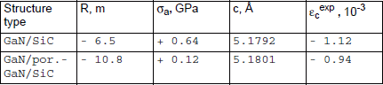
As far as x-ray characterisation was concerned, the calculations of biaxial stresses and strain along c-axis in GaN layers were performed using measured values of radius of curvature R and lattice constant c. The R value was measured as described elsewhere Reference Rozgonyi, Petroff and Panish[8], and the measurements of lattice constants were performed using a triple crystal modification of the Bond method Reference Fewster and Andrew[9]. The measured values of R and lattice constant c (Δc=±0.0001 A) as well as calculated values of biaxial stresses σa and strain εc=(c−c 0)/c 0, where c 0 =5.1850 A is a relaxed lattice constant for GaN Reference Leszczynski, Suski, Perlin, Teisseyre, Grzegory, Bockowski, Yun, Porowski and Major[10], are summarised in Table 2. The data presented in Table 2 show that both GaN layers grown directly on SiC substrate and on porous sublayers were tensile (σa > 0), but tensional biaxial stress and strain in cap layers were significantly reduced as compared to epitaxial layers grown on 6H-SiC.
Radii of curvature,biaxial stresses, lattice constants and strain in the structures studied
Raman scattering measurements were carried out at room temperature using an Ar+ laser (λ=488 nm) as a source of excitation. The scattered radiation was analysed by a double grating monochrometer with computer-controlled systems for scanning and data acquisition. A back scattering geometry with the z direction parallel to the optical axis of the crystal was employed. Figure 4 presents Raman spectra near E2 mode for a GaN layer grown directly on 6H-SiC substrate (a) and for a cap GaN layer (b) grown on porous GaN. The shift of the E2 line towards lower frequencies as compared to its position for a strain-free sample (which in this case was a “bulk” GaN sample grown by HVPE under conditions similar to those described in Reference Melnik, Vassilevski, Nikitina, Babanin, Davydov and Dmitriev[11] with E2 mode peak at 567.8 cm−1) points out to a tensile character of the in-plain stress in the samples studied. At the same time, from Figure 4 it is clearly seen that the shift of the E2 line for a cap layer grown on porous GaN is essentially less than that for a GaN layer grown on 6H-SiC substrate. As estimated from Raman data according to Reference Davydov, Averkiev, Goncharuk, Nelson, Nikitina, Polkovnikov, Smirnov, Jacobson and Semchinova[12], the cap GaN layer had in-plain stress of σ≈0.20 GPa. Fitting the E2 line to the Lorenz function gives the following values for FWHM's in the samples studied: 3.7 cm−1 for GaN layers grown on 6H-SiC substrate and 3.1 cm−1 for cap GaN layers grown on porous sublayer, again supporting the improvement in the crystalline structure of these layers as compared to GaN layers grown directly on SiC substrates.
Raman spectra near E2 mode for a GaN layer grown directly on 6H-SiC substrate (a) and for a GaN layer (b) grown on porous GaN.

The photoluminescence was excited by a pulsed nitrogen laser with 2 kW pumping power. The position of the maximum of luminescence spectra taken at 77 K corresponded to neutral donor-bound exciton recombination in GaN Reference Rieger, Metzger, Angerer, Dimitrov, Ambacher and Stutzmann[13]. This exciton peak maximum for the cap GaN layers was blue-shifted by 22 meV relative to that for GaN layers grown on 6H-SiC, whose maximum corresponded to 3.449 eV. According to Reference Rieger, Metzger, Angerer, Dimitrov, Ambacher and Stutzmann[13], this clearly pointed to a reduction of stress in the cap layer by ~0.9 GPa. Also, the FWHM of the excitonic peak for the cap GaN layer was reduced to as low as 20 meV compared to that of the GaN layer grown on 6H-SiC substrate (FWHM of 32 meV). This feature indicated an improvement in the crystalline structure of GaN layers grown on porous GaN.
Comparison analysis of the x-ray, Raman and PL data shows that the value of the biaxial stresses in cap GaN layers grown on porous sublayers is substantially less than that for the GaN layers grown directly on 6H-SiC substrates. The discrepancy in the absolute values of the biaxial stresses as measured by different methods can be possibly attributed to the fact that these different methods were calibrated using different standards for "strain-free" GaN.
4. Conclusion
Summarizing, GaN layers on porous GaN, for the first time. Porous GaN was formed from GaN layer deposited on 6H-SiC substrate. The crystal structure and stress in GaN layers grown by HVPE on porous GaN was investigated. AFM and RHEED studies showed that the layers possessed smooth surfaces, while PL and Raman measurements pointed to high crystalline quality of the layers. Special emphasis was put on studying the biaxial stresses and strain in the layers. X-ray, Raman and PL measurements showed that the stress in the layers grown on porous GaN was reduced to 0.1-0.2 GPa. Thus, we have shown that porous sublayer allows the growth of high quality GaN with substantially reduced strain as compared to those grown directly on 6H-SiC substrates.
The authors would like to thank Yu. Melnik for GaN epitaxial layers provided for this study, I. Goncharuk and A. Smirnov for Raman measurements, N. Seredova for PL characterizations, V. Busov for SEM characterization and V. Shuman and I. Nikitina for helpful discussions. The work was partially supported by Russian Ministry of Science through a “Surface Atomic Structures“ program and by INTAS grants #96-1031 and #96-2131.


