

1 Introduction
Cubic phase GaN shows several encouraging optical properties Reference Ramirez-Flores, Navarro-Contreras, Lastras-Martinez, Powell and Greene[1] Reference Petalas, Logothetidis, Boultadakis, Alouani and Wills[2] Reference Hong, Pavlidis, Brown and Rand[3] Reference Wu, Yaguchi, Onabe, Ito and Shiraki[4] Reference Godlewski, Bergman, Monemar, Rossner, Langer and Barski[5]. In particular, it was recently suggested that ionization energy of shallow acceptors in cubic GaN is smaller than that observed for shallow acceptors in wurtzite phase GaN Reference Menniger, Jahn, Brandt, Yang and Ploog[6] Reference As, Schmilgus, Wang, Schottker, Schikora and Lischka[7]. If confirmed, this property of cubic GaN can lead to an increased hole concentration in p-type layers and in consequence in more efficient light emitting devices.
In this work we discuss properties of photoluminescence (PL) emission transitions observed in cubic GaN epilayers grown by two modifications of molecular beam epitaxy (MBE) on (001) Si substrates. The influence of surface morphology on “edge” and “red” PL is studied. A strong influence of a grain-type structure of epilayers grown by molecular beam epitaxy (MBE) on edge emissions is demonstrated.
2 Samples
Epilayers of cubic GaN were grown in CEA Grenoble in a RIBER 2300 chamber on (001) Si substrates by two modifications of the MBE method. In gas source MBE (GS-MBE), high purity ammonia was supplied directly to the substrate and was thermally cracked in the presence of gallium. The growth rate was about 0.5 µm/h and the substrate temperature was 800 °C with ECR power of 140Watts. GS-MBE samples were 1- 2 µm thick. Other epilayers were grown using electron cyclotron resonance (ECR) nitrogen cell. Here growth rate was 0.05 µm/h and obtained GaN epilayers were 0.2 - 0.25 µm thick. GS- and ECR-MBE epilayers were grown on AlN, GaN or SiC buffer layers. RHEED patterns indicated a 3D-growth mode for GS-MBE samples and a 2D-growth mode for ECR-MBE samples.
3 Experimental
Low temperature PL and time-resolved PL spectra were measured on a conventional set-up. The 351 nm UV line of an Ar+ laser was used for the cw excitation. Pulsed excitation was provided by a mode locked Ti:sapphire solid-state laser with frequency doubling (λ = 340 nm) with a pulse length of 2 ps. Monochromatic cathodoluminescence (CL) and scanning electron microscope (SEM) images were taken at room temperature in a JEOL JSM-35C scanning electron microscope system with a CL attachment in the accelerating voltage of 25 keV. For such energy of electrons, the primary electrons penetrate through whole the sample.
4 Results and Discussion
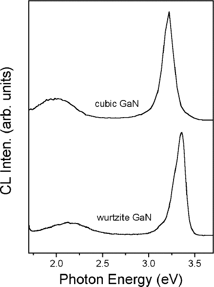
In figure 1 we show the room temperature CL spectrum taken for a cubic GaN epilayer (GS-MBE sample) together with that of the reference spectrum of wurtzite phase GaN (grown by MBE on Si (111) substrate). A close analogy between the two spectra is observed. Both spectra are dominated by a strong edge emission, shifted down in energy by about 200 meV for the cubic epilayer. A similar shift is observed between maxima of the yellow (wurtzite GaN) and the red (cubic GaN) PL/CL emissions. This shift agrees with the difference of band gap energies of two phases of GaN Reference Ramirez-Flores, Navarro-Contreras, Lastras-Martinez, Powell and Greene[1].
Room temperature cathodoluminescence spectra of cubic and wurtzite GaN epilayers grown by the MBE method.
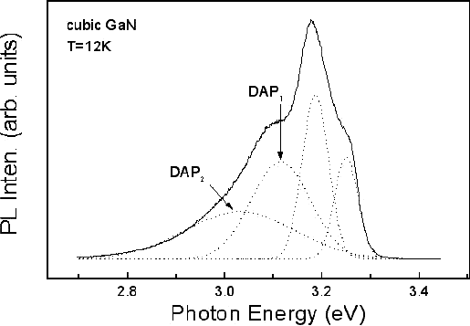
In figure 2 we show a high resolution PL spectrum of cubic GaN sample taken at 12 K. A substructure of the edge emission is resolved and is analyzed by us based on the time-resolved investigation shown in figure 3. This substructure was seen for each of cubic GaN epilayers studied by us and was best resolved for the ECR-MBE sample grown on a thick GaN buffer layer by the metallorganic chemical vapor deposition (MOCVD) method. The position of the observed PL sub-peaks varies slightly from sample to sample, which is probably due to different strain conditions in the epilayers. The detailed time-resolved PL investigations of PL origin were performed for the ECR-MBE sample grown on SiC buffer (figure 3). Two emissions at lower energy show longer PL decay times and are attributed by us to shallow donor-shallow acceptor pair (DAP) transitions. The highest energy sub-peak shows the fastest decay time and is due to excitonic transition (likely due to donor bound exciton). Such identification of the two lowest energy sub-peaks confirms previous reports of lower binding energies of shallow acceptors in cubic GaN than in wurtzite GaN Reference Godlewski, Bergman, Monemar, Rossner, Langer and Barski[5].
Low temperature PL spectrum of a cubic GaN epilayer grown by the ECR-MBE method on a (001) Si substrate covered with a SiC buffer layer.
Time-resolved PL spectrum taken at 2 K under 2 ps pulsed excitation. The spectra were taken at the maximum of PL intensity and after 200 ps and 400 ps of the PL decay.

In figure 4 and figure 5 we show the surface morphology of the GaN epilayers as observed with atomic force microscopy (AFM). AFM scans show the granular structure of cubic GaN epilayers grown by both GS- and ECR-MBE methods. Similar surface morphology is observed by us also for wurtzite GaN films grown by MBE, thus, seems to be a general property of GaN epilayers.
AFM image of the surface morphology of cubic GaN epilayer grown by GS-MBE

AFM image of the surface morphology of a cubic GaN epilayer grown by ECR-MBE.

In the rest of this paper we discuss effects of surface morphology on the edge and red PL emissions of cubic GaN. The first results of such studies for wurtzite GaN are reported in references Reference Zhonghai, Johnson, Mcnulty, Brown, Cook and Schetzina[8] Reference Christiansen, Albrecht, Dorsch, Strunk, Pelzmann, Mayer, Kamp, Ebeling, Zanotti-Fregonara and Salviati[9] Reference Rosner, Carr, Ludowise, Girolami and Erikson[10] Reference Cremades, Piqueras, Xavier, Monteiro, Pereira, Meyer, Hofmann and Fischer[11] Reference Li and Coleman[12]. The granular structure of the surface is reflected in the scanning electron microscopy (SEM) image shown in figure 6. In addition to grains, irregular overgrowth islands were observed similar to the one seen in a corner of figure 6. In figure 7 and figure 8 we show CL scans taken with the detection set at the maximum of the edge and red PL emissions, respectively. Images were recorded at the same region as the SEM image. Whereas the edge emission strongly fluctuates in intensity and is weak at grain boundaries, i.e., in the regions of high dislocation density, the red CL is spatially homogeneous. Such homogeneity of the red CL cannot be explained by signal saturation or by averaging (caused by a long decay time of the red PL). Spot mode CL studies confirm the results shown in figure 8.
Room temperature SEM image at 9000 magnification of the cubic GaN epilayers

Room temperature monochromatic CL image at 9000 magnification of the cubic GaN epilayers taken with the detection set at maximum of the edge emission.

Room temperature monochromatic CL image at 9000 magnification of the cubic GaN epilayers taken with the detection set at maximum of the red emission.

At grain boundaries we expect an increased density of dislocations, which in most semiconductors act as efficient centers of nonradiative recombination. Not surprisingly, edge emission is quenched at grain boundaries. However, the increased density of dislocations apparently affects the intensity of the red emission only weakly. The reasons for spatial homogeneity of the red CL are not understood at present. We point out here that similar spatial homogeneity was recently reported also for the yellow PL of wurtzite GaN Reference Zhonghai, Johnson, Mcnulty, Brown, Cook and Schetzina[8] Reference Godlewski, Goldys, Phillips, Langer and Barski[13]. Thus, our present study indicates that the red PL is a close analogue of the yellow PL of the wurtzite GaN. The yellow emission of wurtzite GaN is explained by the DAP transition of shallow donors and deep acceptors Reference Tansley, Goldys, Godlewski, Zhou, Zuo and Pearton[14]. The origin of the donor and acceptor species participating in the yellow PL is still disputed but none of the models proposed relates this PL to dislocations. We believe that a similar situation is also true for the red PL. One of the possible explanations of otherwise puzzling homogeneity of the red (and yellow) PL/CL is that the defects participating in the red (yellow Reference Zhonghai, Johnson, Mcnulty, Brown, Cook and Schetzina[8]) PL are preferentially generated/accumulated in neighborhood of dislocations, but not at dislocations, since the red CL is not enhanced at grain boundaries.
5 Conclusions
The present PL and time-resolved PL studies confirm recent suggestions on smaller binding energy of shallow acceptors in cubic phase GaN. We further show that edge and red emissions show very different spatial fluctuations of intensity. Whereas edge emissions strongly fluctuate in intensity and are weak at grain boundaries, red emission is spatially homogeneous.
Acknowledgments
This work was partly supported by join project no. 76568 of KBN (Poland) and Ministry of Foreign Affairs (France) and grant numbers 2P 03B 018 13 of KBN


