

I. INTRODUCTION
Wireless power transfer (WPT) technology via microwaves, also known as microwave power transfer (MPT), has advanced since early experiments in the 1960s were conducted by Brown [Reference Brown1]. Recently, inductive coupling WPT and resonance coupling WPT are commercialized for wireless charging of mobile phones and electric vehicles [Reference Shinohara2]. One of the reasons for commercialization of this technology is that lower frequencies (<MHZ) are used for inductive and resonance coupling WPT than those used in MPT (<GHz), which results in higher efficiency and lower cost. However, microwaves can transmit both power and information, and MPT can be used for multipurpose applications, such as high-power WPT and low-power distribution, or multiuser applications. The distance over which wireless power is transferred can also be expanded in the case of MPT. However, the size of transmitting and receiving antennas can theoretically become surprisingly large [Reference Shinohara3]. Therefore, commercialization of MPT has lagged because of the required system size and the cost. In addition, substantial microwave power cannot yet be transmitted under present radio wave regulations, which limit transmission to 1 mW/cm2 in the 2.45 and 5.8 GHz bands owing to questions of safety for humans and other living things exposed to radio waves.
One possible commercial application of MPT is energy harvesting [Reference Hagerty, Helmbrecht, McCalpin, Zane and Popovic4, Reference Sample and Smith5], or a ubiquitous power source [Reference Shinohara, Mitani and Matsumoto6, Reference Maehara7] whose systems involve distributed or broadcasted microwaves rather than microwave beaming. High beam efficiency is not required for these MPT applications.
Another MPT application that reduces theoretical beam efficiency requirements uses MPT in a waveguide. In this application, microwave power does not diffuse as it does in free space, but only propagates through a waveguide. Theoretically, power loss for MPT over a distance in free space depends on diffusion of the radio waves in inverse proportion to the square of the distance. However, the propagation loss in a waveguide does not depend on radio wave diffusion only on the product of the propagation distance and a loss factor, which is a function of the conductivity of the inside surface of the waveguide. This loss is much smaller than the loss incurred in free space propagation. As high-power microwaves can be easily transmitted only along the waveguide, this system results in no interference with conventional wireless communication systems and no radiation-related safety problems for humans and other living things because the microwaves do not propagate in free space. The potential magnitude of microwave power that can be transmitted is then not limited by interference and safety factors but solely by technical issues such as the power limits of semiconductors and microwave circuits.
In this report, we propose MPT for wireless power distribution in a building, rather than wired power distribution, which we have termed a “microwave building” or “wireless building”. The waveguides used to provide microwave power in a microwave building are composed of conventional structures.
II. SYSTEM OF MICROWAVE BUILDING
The proposed wireless power distribution system (WPDS) in a building is illustrated in Fig. 1. Elevation and plane diagrams are shown in Fig. 2. This system wirelessly supplies electrical power using a deck plate consisting of extra cover boards that act as microwave transmission waveguides. A frequency of 2.45 GHz was selected on the basis of the size limitations of the conventional deck plate, and a magnetron was used as the microwave transmitter to reduce cost. Even the cheapest cooker-type magnetron can provide high-quality microwaves that can be used for MPT [Reference Mitani, Shinohara, Matsumoto and Hashimoto8]. The flow of microwave power can be controlled by variable power dividers that supply microwave power only to users requiring it and that block flow to locations where no users exist. Rectennas (rectifying antennas) placed under the floor were used as microwave receivers and DC power sources by converting microwaves to DC power. Adjusting the positions of the rectennas was quite easy because microwaves were present practically everywhere under the floor. The total efficiency from AC grid electricity to DC via microwave transfer was assumed to be 50%. Although the day-to-day running cost of the WPDS for the microwave building system is approximately twice that of a conventionally wired home, the initial cost of the building is reduced because of reduced construction costs. Therefore, it was estimated that the overall lifecycle cost of the building can be reduced by using the WPDS.
Concept of the WPDS for a building.

Elevation and plane diagrams of the WPDS.
In the initial phase, the WPDS is considered for office buildings where DC-driven computers and the other OA (Office Automation) instruments are mainly used. It is estimated that one DC outlet requires <50 W and >3 kW of microwave power must be distributed to each room.
III. PROPAGATION IN A DECK PLATE WAVEGIUDE
A deck plate is conventionally used to support building structures, and it is subject to some standardization. It is essential for this application to choose a standard deck plate as a waveguide. A deck plate is composed of an iron plate having 1.2-mm thickness that is usually gilded with zinc whose thickness is 16.9 µm. The cross-section of a conventional deck plate is a trapezoid where one of the planes is open, as shown in Fig. 3. The open plane must be covered to use the deck plate as a waveguide.
Illustration and photograph of deck plate waveguide.
The results of an electromagnetic simulation of a conventional deck plate with an extra cover board forming a trapezoidal waveguide is shown in Fig. 4. The Ansys HFSS simulator was used. The fundamental TE10 mode of the 2.45-GHz microwave traveling in the waveguide is clearly apparent. The cut-off frequency for the fundamental mode is 1.43 GHz, and the cut-off frequency for the higher mode is 2.86 GHz. The theoretical propagation loss in a rectangular waveguide gilded with zinc is estimated to be 0.018 dB/m. It can be concluded from the simulation that a conventional deck plate can be used as a waveguide at the 2.45-GHz frequency.
Simulation result of the TE10 mode traversing a deck plate waveguide.
A microwave power transmission experiment was conducted to estimate the propagation loss for a conventional deck plate with an extra board to cover the open plane of the deck plate. However, construction efficiency must also be considered because ease of construction is required. We propose three methods to cover the deck plate: spot welding every 150 mm, bolted connection every 150 mm, and solder joints. Solder joints produce optimum waveguides, however, this method has the lowest construction efficiency. Spot welding and the bolted connections are more efficient construction methods but result in less ideal waveguides. The experimental results measured with a 3-m deck plate are shown in Table 1. The loss depends on the method of connection between the deck plate and the cover board. However, the wave propagation loss is almost equal to the theoretical loss. As such, the loss is sufficiently low to warrant the use of a deck plate for the WPDS with low cost.
Experimental results of power loss in a deck plate waveguide.

We have measured microwave leakage from the experimental WPDS using a deck plate as a waveguide. Transmission of a 500-W, 2.45-GHz microwave through a 3-m deck plate yields an average power density of 0.06 mW/cm2 at a distance of 10 cm away from the deck plate and the total leakage microwave power is estimated to be approximately 0.3% of the transmitted power.
IV. POWER DISTRIBUTION FROM THE CENTRAL WAVEGUIDE TO DECK PLATE WAVEGUIDES
As shown in Figs 1 and 2, the generated microwave power is initially propagated in a central waveguide located in a wall and is thereafter distributed to the deck plate waveguides under the floor. This is the most effective point in the system from which to control the power distribution in accordance with user requirements.
Initially, the variable power divider illustrated in Fig. 5 was developed with movable dielectric walls. The power divider is inserted between the deck plate waveguides and the central waveguide connected to the magnetron. The S parameters were simulated and measured (Figs 6(a) and 6(b)) with the x and m parameters shown in Fig. 5(b). A power distribution ratio from −10 to −3 dB is achieved. Using this system, the microwave power delivered to each deck plate waveguide line can reflect user load. This means that the WPDS can adapt to changing loads. The load changing will be estimated by measuring the change of reflected microwave parameters. The power dividers will be controlled with wireless information, for example Bluetooth.
(a) Photograph and (b) illustration of the developed power divider.
Simulated and measured S 11, S 21, and S 31 with x and m parameters.
V. RECTENNA OUTLET
Finally, the propagated microwave power is acquired from the deck plate, converted from microwave to DC, and made available for use. This module is called a “rectenna outlet” (Fig. 7(a)). To acquire the microwave power, we propose using a coaxial probe. The simulated S parameters of the coaxial probe, using the length l of the probe as a parameter, are shown in Fig. 8. The simulation results indicate that the acquisition of microwave power can be controlled by changing the value of l. This functionality is sufficient for the rectenna outlet.
(a) Block diagram of the rectenna outlet, (b) detail of the microwave pick-up.
Simulated S parameters for transmission from the deck plate to the coaxial pick-up.
On the basis of the simulation, four pick-ups were located on a 3-m deck plate waveguide (Fig. 9) to test the WPDS. Figures 10(a) and 10(b) illustrate the simulated and measured S parameters, respectively, of the system shown in Fig. 9. Power differences in each port are 0.3 dB at 2.45 GHz by simulation and 0.4 dB at 2.434 GHz by measurement. Each port is connected to 50 Ω. The end of the deck plate waveguide is shorted. At the last port (port 5) closest to the shorted end, a conventional waveguide-coaxial converter is used.
An illustration of the four pick-ups located on a 3-m deck plate waveguide.
S parameters for each port shown in Fig. 9: (a) simulation and (b) measurement.
For this system, we require a highly efficient rectenna providing for a high DC power output of approximately 100 W. To this end, we have developed two types of the high-power rectennas. One rectenna is composed of conventional Si Schottky barrier diodes. The other is a rectenna developed with GaN Schottky barrier diodes.
The conventional Schottky barrier diode rectenna rectifies approximately 1 W only. Therefore, a T-junction power divider is used to decrease the input microwave power to each Schottky barrier diode. To achieve 100 W of rectified power with a single rectenna, we developed a rectenna composed of a 64-way power divider with 256 (=64 × 4) diodes, as shown in Fig. 11. The loss of the power divider was experimentally determined to be <5%. We used a single-shunt-type rectifier as a full-wave rectifier with only one diode. We used four diodes, two in series and two in parallel, for a single rectifier element. The rectifier can provide 55% RF–DC conversion efficiency at an input microwave power of 100 W (Fig. 12). The size of the rectifier circuit was 125 mm in length, 110 mm in width, and 95 mm in height.
Developed 64-divided high-power rectenna composed of 256 Si Schottky barrier diodes.
RF–DC conversion efficiency of high-power rectenna in the case of 64-parallel connections and a load of 10 Ω.
For the rectenna outlet, a power buffer is required to stabilize the supplied DC power. We developed the rectenna outlet with a DC/DC converter and batteries as shown in Fig. 13. It is sufficient to supply <50 W DC at the outlet. However, it is necessary for this application to develop higher efficiency and smaller-sized rectenna outlets. The efficiency and the size are limited for a rectenna composed of 256 diodes. An efficiency of 74.8% at 191 mW was experimentally obtained using the described Si Schottky barrier diodes, however, for technical reasons, increasing the number of diodes means decreasing efficiency. In addition, the size of a rectenna composed of many diodes cannot be decreased.
Rectenna outlet composed of a rectenna, a DC/DC converter and batteries.
As can be seen from Figs 11 and 13, the conventional rectenna outlet is too big to be used in the WPDS system. To increase the efficiency and decrease the size of the rectifier, low parasitic capacitance Schottky diodes with low ON resistance, low ON offset voltage, and high reverse breakdown must be developed. To this end, we are developing lateral GaN Schottky diodes (Fig. 14) [Reference Takahashi9]. The target frequency is set at 2.45 GHz, and the handling power of a single diode is less than 10 W with a breakdown voltage of 100 V.
(a) Device structure of an n-GaN Schottky diode on an SI SiC substrate. (b) Photograph of fabricated diode with five anode fingers [9]. (c) Photograph of the GaN diodes.
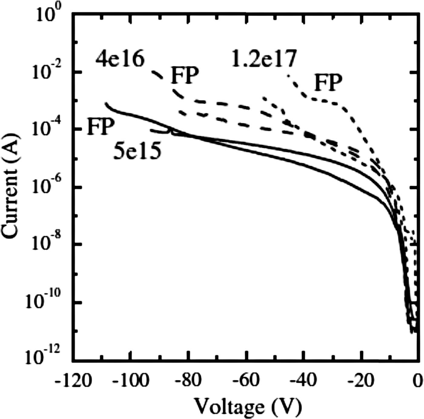
Figure 15 shows the reverse I–V characteristics of single finger diodes. The curves marked “FP” are for the with-field plate structure, whereas the other curves are for the without-field plate structure for the same device. As shown in the figure, the devices with the field plate have slightly higher breakdown voltages, except for the high-concentration sample. The breakdown voltages for those with the field plate reach 108 and 93 V for doping levels of 5.0 × 10¹⁵ and 4.0 × 1016 cm3, respectively. When the doping level is over 1.0 × 1017 cm3, the breakdown voltage decreases to approximately 50 V.
Breakdown characteristics of diodes under reverse bias [9].
We developed a rectifier composed of GaN diodes of V br = 100 V and ten fingers (Fig. 16), and the RF–DC conversion efficiency was measured (Fig. 17). The input impedance was matched at each microwave input. An efficiency of 74.4% was achieved with a 5-W, 2.45-GHz input for a single GaN diode. This indicates that a 100 W rectenna can be developed with 15–20 GaN diodes only. In fact, it is possible to develop a 100 W rectenna with just a single GaN diode.
GaN diode rectifier of V br = 100 V and ten fingers: (a) illustration and (b) photograph.
Measured RF–DC conversion efficiency of rectifier composed of a GaN diode.
Final test setup: (a) frame, (b) deck plate waveguide, (c) concrete at floor, (d) power distributor, (e) final setup.
VI. TOTAL SYSTEM EXPERIMENT
Finally, the total WPDS was built in the laboratory, and experiments were conducted on the total system. A photograph of the experimental configuration is shown in Fig. 18. A 3.2 × 3.2 m room was emulated that contained four office desks. A 2.45-GHz, 1.5-kW microwave was transmitted in the WPDS and successfully received at the rectenna outlets. The efficiency of each system element was estimated as follows:
(1) microwave generation at magnetron: 82%;
(2) power distribution: 95%;
(3) propagation in deck plate waveguide: 95%;
(4) microwave pick up and rectifier: 74%;
(5) system control: 95%;
(6) total: 52%.
The total efficiency is sufficient for initial development. We estimate a total cost of the WPDS with the experimental efficiency and we conclude that the total cost of the WPDS is the same or less than a conventional wire power distribution in a building.
VII. CONCLUSION
We proposed a WPDS for a building as an application of MPT. The cost of the system is one of the important factors to determine whether the WPDS will be applied or not. We have estimated the cost and compared it with that of a conventional building. We assumed 40 years life cycle of both conventional and WPDS buildings. We assume in the conventional building that the renewal cycle of wired power distributions is 10 years and that AC/DC converters with 40% efficiency, which is a typical value, are used in all electrical products. On contrary, we assume in the WPDS that the renewal cycle of batteries, electrical and mechanical parts are 5, 20, and 40 years, respectively. The efficiency of the WPDS is assumed 50%. As a result of the cost estimation, the cost of the WPDS is 0.98 against the cost of the conventional building which is normalized to 1. It is a fair and hopeful estimation for users who consider using the WPDS instead of the wired power distribution taking into account that the WPDS has the additionally merit of free positioning of power outlets.
In the WPDS, wireless microwave power propagates in waveguides. The usage of a waveguide alleviates the problems associated with large-sized antennas for high-efficiency beam MPT and radio wave regulations and allows for MPT commercialization. The total cost of buildings can be reduced over their entire lifespan with use of the WPDS. Therefore, the WPDS is one of the first promising applications of MPT.
ACKNOWLEDGEMENT
This work was supported by the Innovative Technology Development Fund of Japan Science and Technology Agency (JST).
Naoki Shinohara received his B.E. degree in Electronic Engineering, the M.E. and Ph.D. (Eng.) degrees in Electrical Engineering from Kyoto University, Japan, in 1991, 1993, and 1996, respectively. He was a research associate in the Radio Atmospheric Science Center, Kyoto University from 1998. He was a research associate of the Radio Science Center for Space and Atmosphere, Kyoto University by recognizing the Radio Atmospheric Science Center from 2000, and there he was an Associate Professor since 2001. He was an Associate Professor in Research Institute for Sustainable Humanosphere, Kyoto University by recognizing the Radio Science Center for Space and Atmosphere since 2004. From 2010, he has been a Professor in Research Institute for Sustainable Humanosphere, Kyoto University. He has been engaged in research on Solar Power Station/Satellite and Microwave Power Transmission system.
Naoki Niwa received his B.E. degree in Structural Engineering from Tsukuba University in 1982, and Ph.D. (Eng.) degree in Structural Engineering from Tsukuba University in 2000. He joined the Kajima Corporation in 1982, and has worked on the design of building structure. He was a research engineer of Kobori Research Complex, working on seismic response control from 1988. From 2003, he has been a chief research engineer in Kajima Technical of Research Institute (KaTRI), Kajima Corporation. He has been engaged in research on wireless power transfer in buildings, energy conversion, and seismic response control. In addition to his research activities, he worked on the project management of newly designed KaTRI H.Q. building. He has been a part-time lecturer, Tsukuba University from 2004. He is a P.E.Jp (Civil Engineering) and structural design 1st class architect.
 Kenji Takagi received his B.E. degree in Mechanical Engineering from Keio University in 1986, and Ph.D. (Eng.) degree in Architecture and Building Science from Tohoku University in 1998. He joined the Kajima Corporation in 1986, and has worked on research of thermal fluid analysis. He was a researcher of Kajima Technical of Research Institute (KaTRI), Kajima Corporation from 1986. He was a visiting scientist in Lamont-Doherty Earth Observatory of Columbia University from 1993 to 1994. He was a chief research engineer of KaTRI since 2005 and a lead researcher of Advanced Technology Incubation and Mechatronics Group of KaTRI since 2013. He has been engaged in research on wireless power transfer in buildings, energy conversion, and external wind forces to building.
 Kenniti Hamamoto received his B.E. degree in Mechanical Engineering from Kyoto University in 1995 and Ph.D. (Informatics) degree in Systems Science from Kyoto University in 2000. He joined Kajima Technical of Research Institute (KaTRI), Kajima Corporation in 2001, and has worked on the study of automonous control systems for building and civil construction equipments. Since 2004, he has been a Senior Research Engineer in KaTRI. He has been engaged in research on control for a power distribution system in buildings and control systems for civil construction equipments.
Satoshi Ujigawa received his B.E. degree in Electrical and Electronic Engineering from Chiba University in 1999, M.E. degree in Natural Science from Chiba University in 2001, and Ph.D. (Eng.) degree in Electromagnetic Wave Engineering from Chiba University in 2011. He joined Kajima Technical of Research Institute (KaTRI) of Kajima Corporation as a research engineer in 2006, and has worked on Electromagnetic Compatibility in building environment. From 2013, he has been a Senior Research Engineer and a 3rd Class Electrical Chief Engineer. He is a member of the Institute of Electrical and Electronics Engineers (IEEE) EMC, AP, MTT, and MAG societies, and of American Geophysical Union(AGU).
 Jing-Ping Ao received his B.S. degree in Physics in Wuhan University in 1989, Wuhan, M.S. degree in semiconductor physics and semiconductor device physics in Hebei Semiconductor Research Institute (HSRI) in 1992, Shijiazhuang, and Ph.D. degree in Electronic Engineering from Jilin University in 2000, Changchun, China. He joined HSRI in 1992, working on high-speed compound semiconductor devices and integrated circuits, optoelectronic devices and optoelectronic integrated circuits. He joined The University of Tokushima, Japan, in February 2001, and currently he is an Associate Professor involved in the research and development of wide bandgap semiconductor (gallium nitride etc.) electronic devices, monolithic integrated circuits, chemical sensor, and optoelectronic devices. He has published more than 120 scientific papers, chapters of book and international conference presentations. He holds several patents on gallium nitride light-emitting diodes and electron devices. He was invited for scientific lectures by prestigious universities and institutes for more than 20 times. Dr. Ao is a senior member of the IEEE and a member of The Electrochemical Society, The Japan Society of Applied Physics and The Institute of the Electronics, Information, and Communication Engineers.
Yasuo Ohno received his B.A. degree in Pure and Applied Science from Tokyo University in 1970, and his Ph.D. degree in Electrical Engineering from the Tokyo Institute of Technology in 1994. He joined NEC Corporation in 1970, and has worked on semiconductor devices including silicon LSIs, GaAs LEDs and FETs, and GaN FETs. He joined the University of Tokushima in 2001. He was a Professor in the Institute of Technology and Science, and worked on the research of GaN power devices and its application to microwave systems. In 2012, he established e-Device, Inc. in Sapporo, Japan, and now a director of e-Device, Inc. Dr. Ohno is a member of the Japan Society of Applied Physics and the IEEE, a fellow of the Institute of Electronics, Information, and Communication Engineers (IEICE).