


1. Introduction
Additive Manufacturing (AM) offers significant design freedom for products with functional integration, complex geometries and hierarchical structures (Reference Gibson, Rosen, Stucker and KhorasaniGibson et al., 2021; Reference RosenRosen, 2007). Among these technologies listed in DIN EN ISO/ASTM 52910:2020-02, Material Extrusion (MEX-TRB/P) of polymers is particularly relevant due to its selective material deposition enabling complex multi-material structures. This capability is increasingly used to realise electrical functions with conductive polymer composites (CPC), including current-carrying leads and Joule-heating elements.
Most work emphasises materials and processing (Reference Masarra, Batistella, Quantin, Regazzi, Pucci, El Hage and Lopez-CuestaMasarra et al., 2022; Reference Nowka, Hilbig, Schulze, Heller, Goutier and VietorNowka et al., 2024; Reference Paz, Moriche, Monzón and GarcíaPaz et al., 2020; Reference Stankevich, Sevcenko, Bulderberga, Dutovs, Erts, Piskunovs, Ivanovs, Ivanov and AniskevichStankevich et al., 2023; Reference Truman, Whitwam, Nelson-Cheeseman and KoernerTruman et al., 2020; Reference Watschke, Hilbig and VietorWatschke et al., 2019) while a few studies explore the impact of the design of the electrical structures on the resulting product performance (Reference Barši Palmić, Slavič and BoltežarBarši Palmić et al., 2020; Reference Kim, Park, Suh, Kim, Jeong and ParkKim et al., 2017; Reference Kwok, Goh, Tan, Tan, Tjiu, Soh, Ng, Chan, Hui and GohKwok et al., 2017; Reference Nassar and DahiyaNassar & Dahiya, 2021; Reference Tan and LowTan & Low, 2018). A systematic investigation of basic design principles has not been conducted.
Fundamental Design for Additive Manufacturing (DfAM) guidelines are therefore missing for three interdependent structure types: low-loss conductors, heating elements with spatially controlled, homogeneous heat generation and transitions that suppress localised hotspots. This work addresses this gap by experimentally investigating 2D and 2.5D geometric factors and by linking path planning to current-density homogeneity. Based on resistivity measurements and thermographic analysis, practical design rules are derived, supporting higher conductivity, reduced hotspots, and more robust products and forming a basis for standardised DfAM of electrically functional MEX structures.
2. Acquisition of data for the design exploration approach
The following section presents the design of experiments, the set-up of the Additive Manufacturing process and the experimental design.
2.1. Materials, processing by additive manufacturing and specimen preparation
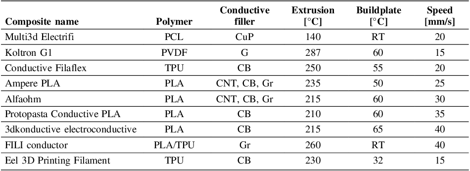
Table 1 provides an overview of the electrically conductive composites used, including their composition and the constant processing parameters used for the manufacturing of specimens.
Overview of the composites and AM processing parameters

Polymers: PCL = polycaprolactone; PLA = polylactic acid; PVDF = polyvinylidene fluoride, TPU = thermoplastic polyurethane. Conductive fillers: CuP = copper particles; G = graphene; CNT = carbon nanotubes; CB = carbon black; Gr = graphite. RT = room temperature (23 ± 1°C).
Before additive processing, all filaments were dried for 48 hours. The specimens were fabricated using a toolchanger system equipped with Hemera direct drive filament extruders and hardened, coated 400 µm nozzle X (E3D-Online, Chalgrove, Oxfordshire, United Kingdom). The G-code was generated using SuperSlicer 2.4 (based on PrusaSlicer, Prusa Research, Prague, Czech Republic). Following the recommendations of Reference Nowka, Ruge, Hilbig, Schulze and VietorNowka et al. (2025) for CPCs the layer height (200 µm) equaled 50% of the 400 µm nozzle diameter. The thickness of the specimens was measured and only those within the ± 5% tolerance range defined by DIN EN ISO 3915:2022-5 are included in the analysis.
To minimise the contact resistance colloidal silver ink EMS#12640 (Electron Microscopy Sciences, Hatfield, PA, USA) was used as an electrical bonding agent. For Koltron G1, to which the ink does not adhere, conductive epoxy 8331D-14G (MG Chemicals Ltd., Burlington, ON, Canada) was used.
2.2. Test rig for the resistance measurement and thermography
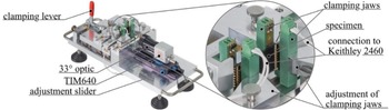
Depending on the objective, the specimens are analysed for either their resistivity or heat distribution within electrically conductive structures. The test rig (Reference Nowka, Hilbig, Schulze, Heller, Goutier and VietorNowka, Ruge, et al., 2024) is shown in Figure 1:
Test rig for electrical resistance measurements and thermographic imaging

Figure 1 Long description
A test rig for electrical resistance measurements and thermographic imaging. The rig includes a clamping lever, 33 degrees optic TIM640 adjustment slider, clamping jaws, specimen, connection to Keithley 2460, and adjustment of clamping jaws.
The test rig utilises spring-loaded contacts, ensuring repeatable testing conditions such as consistent contact force between the specimen and the source meter. Electrical resistance is measured according to DIN EN ISO 3915:2022-5 using a four-wire measurement technique with a Keithley 2460 Sourcemeter (Keithley Instruments, Solon, OH, USA) at 23 ± 1°C and a measurement current of 100 µA. The resistivity ρ is calculated from the measured resistance R, the conductive cross-sectional area A and the length L between the inner contact surfaces using the following Equation (1):

The reciprocal of resistivity ρ is called conductivity σ. The evaluation of current density homogeneity is conducted qualitatively using thermographic imaging. Areas with higher current density are expected to exhibit elevated temperatures. To ensure comparability, the specimens are heated with a constant power and once the rated power is reached within ± 2%, a thermogram is taken automatically with a defined delay. Thermal images are recorded using a TIM 640 thermal imaging camera (640 × 480 px) with 33° optics (Micro-Epsilon Messtechnik GmbH & Co. KG, Ortenburg, Germany) at object distances of 100 mm and 125 mm, yielding resolutions of approximately 62 µm/px and 77.5 µm/px, respectively.
2.3. Influence of number of strands on resistivity
The width of electrically conductive structures affects their cross-sectional area, making it a critical design parameter. Two studies suggest that the number of parallel strands can significantly influence the resistivity of structures made by MEX (Reference Truman, Whitwam, Nelson-Cheeseman and KoernerTruman et al., 2020; Reference Zhang, Yang, Fu, You, Dong and DaiZhang et al., 2017). Therefore, an extensive study with nine composites and finer strand-number gradations was conducted. Rectangular (60 × 24 mm), single-layer (200 µm) specimens with 0° infill to the measurement direction were fabricated. Figure 2 shows representative specimens and the schematic measurement setup.
Alfaohm specimens with 1 to 67 strands (from left to right)

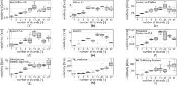
The number of parallel strands was varied, producing specimens with 1, 2, 3, 5, 8, 13, 21, 34, and 67 strands. For each parameter set, seven specimens were fabricated. The results are presented in Figure 3:
Influence of number of strands on resistivity across composites: (a) Multi3d Electrifi; (b) Koltron G1; (c) Conductive Filaflex; (d) Ampere PLA; (e) Alfaohm; (f) Protopasta Conductive PLA; (g) 3dkonductive electroconductive; (h) FILI conductor; (i) Eel 3D Printing Filament

Figure 3 Long description
Panel A: A box plot shows the resistivity in ohm centimeters (Ωcm) of Multi3d Electrifi as the number of strands increases from 1 to 67. The resistivity generally increases with the number of strands, showing variability and outliers. Panel B: A box plot illustrates the resistivity of Koltron G1, which also increases with the number of strands, displaying a similar trend of variability and outliers. Panel C: A box plot for Conductive Filaflex shows a significant increase in resistivity as the number of strands increases, with notable variability and outliers. Panel D: The box plot for Ampere PLA indicates an increase in resistivity with the number of strands, with visible variability and outliers. Panel E: A box plot for Alfaohm shows a moderate increase in resistivity with the number of strands, with some variability and outliers. Panel F: The box plot for Protopasta Conductive PLA depicts an increase in resistivity with the number of strands, showing variability and outliers. Panel G: A box plot for 3dkonductive electroconductive shows a substantial increase in resistivity with the number of strands, with significant variability and outliers. Panel H: The box plot for FILI conductor indicates an increase in resistivity with the number of strands, with visible variability and outliers. Panel I: A box plot for Eel 3D Printing Filament shows an increase in resistivity with the number of strands, displaying variability and outliers.
All composites show the lowest resistivity for single-strand conductors. With increasing strand count, resistivity first rises, then either reaches a plateau (Figure 3a–g) or continues to increase (Figure 3h-i), indicating that the chosen parameter range may be too narrow for some materials. In all cases, variability grows with strand number. Alfaohm, combining high conductivity with low variance, was used in subsequent experiments.
2.4. Influence of conductor design on current-density homogeneity
The primary function of electrical conductors is to transmit current between two points with minimal losses. This experimental series aims to determine the influence of 2D and 2.5D geometric factors on the homogeneity of current distribution within the conductor.
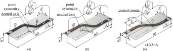
To approximate a path-planning strategy aligned with the current flow, all strands are deposited parallel to the neutral axis (Figure 4), thereby avoiding adverse effects of inter-strand contact resistance. Extrusion process parameters (Table 1) are kept constant. The specimens are 5 mm wide, 200 µm thick, manufactured as single-layer structures made from Alfaohm, and both contact areas are coated with silver ink to minimise contact resistance between the specimen and the measurement setup.
The varied design parameter in this study is the conductor geometry. Discontinuous layouts and continuous layouts based on Bézier splines are investigated. For discontinuous conductors, the varied design factors are the deflection angle θ (30°–120° in 15° increments) from the straight path and the corner modification. Bisecting chamfers (lengths 1, 2, 5, 10 mm) and fillets (radii 1, 2, 5, 10 mm) are examined. For Bézier splines, the aspect ratio A (1, 2, 3) and the relative control point position dcp (25%–100% in 25% increments) are varied, with tangential continuity enforced at the start and end points. The design concepts and measurement setup are shown in Figure 4.
Design concepts for AM conductor path planning: (a) discrete with radius; (b) discrete with chamfer; (c) continuous Bézier spline

Geometry and dimensions influence the current distribution and, consequently, the heat generation within the conductors. The evaluation is based on thermographic imaging. Thermographic images are recorded at a power input of 1500 mW with a trigger delay of 1 s. The short duration between the onset of heating and image acquisition ensures that the results are only marginally affected by heat conduction from local hotspots to cooler regions. The following figures present the thermograms obtained from the three experimental series.
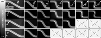
Figure 5 shows thermograms of discontinuous conductors with radii as corner modifications.
Thermographic images of specimens with discontinuous paths (see Figure 4a), for varying angles θ and radii R. Recorded at 1500 mW after 1 s. ☒ = geometrical not realisable

The thermographic images in Figure 5 reveal two key trends. First, sharper deflection angles generate more pronounced hotspots on the inner edge of the conductor, accompanied by corresponding cold spots on the outer edge. These cold spots, located opposite the hotspots, exhibit significantly lower temperatures and thus indicate a reduced contribution to current transport. Second, increasing the corner radius decreases hotspot intensity and distributes the elevated temperature over a larger area, indicating a reduction in local current density.
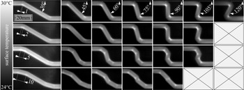
Figure 6 shows thermograms of discontinuous conductors with chamfers as corner modifications.
Thermographic images of specimens with discontinuous paths (see Figure 4b), for varying angles θ and chamfer lengths a. Recorded with 1500 mW after 1 s. ☒ = geometrical not realisable

Figure 6 Long description
The image contains multiple thermographic images arranged in a grid. The grid is organized with angles increasing from left to right (30 degrees to 120 degrees) and surface temperatures decreasing from top to bottom (30 degrees Celsius to 24 degrees Celsius). Each cell in the grid shows a thermographic image of a specimen with a discontinuous path. The images capture the heat distribution along the path at different angles and temperatures. The images are labeled with the angle and chamfer length. Some cells are marked with a cross pattern indicating geometrically non-realizable configurations.
As with the radii, two trends are evident. First, larger deflection angles θ lead to more pronounced hotspots. Chamfers generally reduce hotspot intensity by smoothing sharp transitions. However, their effect is notably weaker than that of radii. Even for large chamfer lengths, distinct hotspots remain. Compared to hotspots formed by radii (cf. Figure 5), hotspots occurring in chamfered regions appear sharper and extend over a larger portion of the track width.
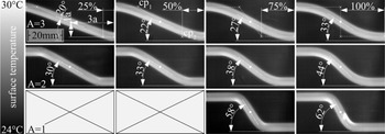
Figure 7 shows the thermographic images of continuous conductors following Bézier spline paths.
Thermographic images of specimens with continoues Bézier splines shown in Figure 4c, with varying aspect ratios A (=a1/a2) and control point (cp) distances. Recorded with 1500 mW after 1 s. The tangent slope angles serve as reference for comparison. ☒ = geometrical not realisable

At first glance, spline-based conductors appear more homogeneous than the previously discussed layouts. However, a visual comparison of the tangent slopes between the two turning points reveals that the hotspot characteristics are similar to those of discontinuous paths with comparable local gradients. This is particularly evident for spline variants with an aspect ratio A = 1 and control point distances of 75% and 100%, which closely resemble the behaviour of the 60°/R2 radius configuration (cf. Figure 5). Splines therefore do not inherently outperform or underperform comparable discontinuous geometries with radii. Instead, their main advantage lies in robustness and usability: spline paths between defined start and end points are generated automatically according to boundary conditions, making them less sensitive to dimensional changes and reducing the need for expert tuning of geometric parameters.
2.5. Design of heat generating structures
Heating structures are intended to convert electrical energy into (homogeneously distributed) thermal energy within a targeted area. The objective of this experimental series is to investigate various design approaches for spatially localised and homogeneous heat generation. The thermal power P generated by an additively manufactured heating structure can be influenced by a combination of design and manufacturing parameters, as expressed in Equation (2):

Here, the voltage drop ΔU across the heating structure is determined by the external system voltage and the resistances of other components in the circuit. The overall resistivity ρ of the structure depends significantly on the feedstock resistivity ρF (Reference Nowka, Hilbig, Schulze, Jung and VietorNowka et al., 2023), the path planning parameters B1...n (Reference Nowka, Ruge, Hilbig, Schulze and VietorNowka et al., 2025) and the extrusion parameters P1...n (Reference Nowka, Hilbig, Schulze, Heller, Goutier and VietorNowka et al., 2024) used during the additive manufacturing process. While the influence of these AM parameters on the resulting resistivity has been extensively studied (Reference Barši Palmić, Slavič and BoltežarBarši Palmić et al., 2020; Reference Paz, Moriche, Monzón and GarcíaPaz et al., 2020; Reference Stankevich, Sevcenko, Bulderberga, Dutovs, Erts, Piskunovs, Ivanovs, Ivanov and AniskevichStankevich et al., 2023; Reference Watschke, Hilbig and VietorWatschke et al., 2019), this work focuses on the geometric factors, specifically the effective conductor length L and the cross-sectional area A, which directly impact the overall electrical resistance. Figure 8 groups the concepts into several categories and illustrates specific implementation variants for each.
Design concepts for heating structures in additive manufacturing

The group of path-planning concepts comprises several approaches to increase resistivity by controlling material placement. On the microscopic scale, resistivity can be increased by arranging strands in close proximity and thereby raising the overall resistance, as discussed in Section 2.3. On the mesoscopic scale, intentionally interrupting individual strands forces the current through inter-strand contact interfaces, increasing contact resistance and thus heat generation within and between layers. On the macroscopic scale, the current path is further manipulated by separating larger strand bundles, forcing current through orthogonal infill patterns, which exhibit higher resistivity than parallel arrangements (Reference Hohimer, Petrossian, Ameli, Mo and PötschkeHohimer et al., 2020).
Local resistance can also be increased by reducing the electrically conductive cross-sectional area A, either by decreasing strand height or width in the heating region. A further option is to extend the effective conductor length L using meander-like paths, which enforce a longer, more resistive current trajectory.
Due to differences in volume and surface area, the thermograms of the heating structures are not directly comparable in a quantitative manner. To enhance qualitative comparison, all specimens are driven at 750 mW, and thermograms are recorded after 30 s, ensuring that the temperature distribution has reached steady state. The resulting temperature distributions are shown in Figure 9.
Infrared thermograms of various heating structures: (a) reference; (b) microscopic; (c) mesoscopic; (d) macroscopic; (e) height variation; (f) width variation; (g) meander

The microscopic heating structure (Figure 9b) relies on locally concentrated strand arrangements to tailor resistivity and exhibits well-defined, localised, and homogeneous heating. The mesoscopic structure (Figure 9c) is geometrically similar to the plate-like reference heater (Figure 9a) yet exhibits slightly less homogeneous heating due to contact resistance at internal transitions. The design with macroscopic slots (Figure 9d) shows pronounced hotspots at the slot edges. The upper and lower regions conduct along the strand direction, while the central region forces current perpendicular to the strands through higher inter-strand contact resistance, resulting in targeted heating but hotspot prone transitions. The vertical taper (Figure 9e) enables the most precise heat localisation, as the discrete reduction in cross-section in 200 µm steps along the build direction (staircase effect) produces well-defined heating zones. In contrast, the horizontal taper (Figure 9f) yields more diffuse edge heating due to the continuous cross-sectional change in the xy-plane. Several specimens (Figures 9a and c) distribute the applied power over a larger area and therefore appear cooler.
2.6. Design of transition structures between different geometries
Heating structures are often large-area by design to achieve good heat transfer, whereas conductors are kept compact to conserve space. This necessitates transition structures that enable a continuous change in both geometry and electrical resistance between conductor and heater, thereby avoiding hotspots in the transition region. An ideal transition exhibits high spatial selectivity: the conductor region remains cold, while the temperature at the beginning of the heating structure matches that of the remaining heater. Various concepts for such transition structures are shown in Figure 10.
Design concepts for continuous transition structures between electrically conductive elements of dissimilar geometry

The simplest approach to increase the transition area is a straightforward widening of the conductor to the full width of the heating structure while maintaining the 0° infill orientation of the conductor. An improved variant, the so-called filled concept, distributes the conductive strands equidistantly and fills the remaining gaps with parallel strands to promote a more uniform current distribution. Another concept keeps the total cross-sectional area constant by varying strand width and height. Fan-out concepts deliberately split and spread individual strands to avoid local constrictions; in the symmetrical and balancing variants, all strands additionally share the same length. A special case is the direct transition from a conventional conductor to an additively manufactured heating structure.
Depending on the design, these concepts are suited for different heater types. Fan-out concepts are particularly suitable for meandering or highly branched layouts such as the microscopic, mesoscopic, and meander structures (cf. Figure 8), whereas cross-section and direct approaches are preferred for planar heaters such as the reference, macroscopic, or variable height and width structures. Figure 11 shows thermographic images of transitions from a conductor to a heating structure.
Thermographic images of transition structures: (a) transition without modifications (reference); (b) not investigated; (c) constant cross-section; (d) flared transition; (e) symmetric flaring; (f) flaring with length compensation; (g) direct contact

Figure 11 Long description
Panel A: A thermographic image of a transition structure without modifications, serving as a reference. The image shows a cross-sectional view with dimensions labeled as 30 millimeters. Panel B: A diagram of a transition structure with a cross shape, not investigated in this context. Panel C: A thermographic image of a transition structure with a constant cross-section. Panel D: A thermographic image of a transition structure with a flared design. Panel E: A thermographic image of a transition structure with symmetric flaring. Panel F: A thermographic image of a transition structure with flaring and length compensation. Panel G: A thermographic image of a transition structure with direct contact, highlighting a defect area with a copper foil.
The transition structure in Figure 11a widens the conductor to the heater width at a constant 0° infill angle and serves as reference. The concept in Figure 11b is based on fanning out individual strands and filling the gaps but was not fabricated or evaluated due to its complex path planning. The heater in Figure 11c uses a geometric transition: the current supplying conductor is manufactured in multiple layers and becomes thinner as it widens toward the heater. Owing to the larger conductive cross-section, the losses and consequently the temperature in the conductor and transition region are significantly lower than in the heating zone. The concepts in Figures 11d to f fan out the strands equidistantly, with basic, symmetrical, and length-balanced layouts. This results in a more homogeneous current density in the heater. The design in Figure 11g is unique in that the heating structure is printed directly onto a conventional conductor, which simultaneously functions as the external electrical interface. Due to the high conductivity of the conventional lead, losses occur primarily at the interface, while the additively manufactured heater exhibits a highly uniform temperature and current-density distribution.
3. Derivation of design guidelines from the experimental data
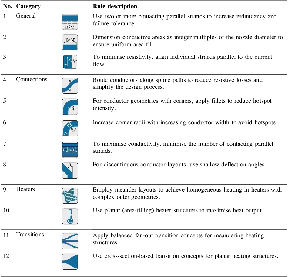
Based on the experimental findings, design guidelines for AM can be derived. Table 2 summarises these guidelines in four categories: general recommendations, which apply universally, and specific guidelines for conductors, heating structures and transition structures.
Design for Additive Manufacturing guidelines for electrically conductive structures derived from experimental data

Some design guidelines are inherently conflicting. For example, increasing reliability by using multiple parallel paths opposes minimising specific resistance by reducing the number of adjacent strands. Depending on the design objective, the relevance and weighting of individual guidelines must therefore be carefully balanced.
4. Application example
As a practical application, a non-heated mirror is modified with an additively manufactured backside heating structure. The goal is to integrate the heater without redesigning the mirror mount, ensuring the surface reaches at least 35°C to evaporate condensed water. To avoid additional insulation or touch protection, the system is designed for 10 W peak power at a voltage below 60 V ensuring electrical safety. A meander-shaped heater is selected to cover the irregular backside with a compact footprint while maintaining homogeneous heating. It is divided into two zones with equal electrical resistance and thus identical heating power. The meander amplitude is adapted to maintain constant resistance along each branch, avoiding hotspots. A fanned-out transition connects the main conductor to the heater. The electrical interface is realised with conductive epoxy. The demonstrator is shown in Figure 12.
Demonstrator: (a) design concept; (b) validation of the Joule-heating structure by thermography; (c) integrated modified mirror in assembly

The convex backside of the mirror results in a non-planar surface for the MEX process. The surface is therefore probed, and the measured profile is used to adapt the nozzle distance during extrusion, ensuring uniform layer thickness and adhesion. Thermography (Figure 12b) confirms homogeneous heating, and Figure 12c shows the integrated system in the assembled state.
5. Conclusion
This study established foundational design guidelines for conductors, Joule-heating structures and as a novel design aspect their transitions fabricated using MEX. The key findings are derived from experimental resistivity measurements, thermographic analysis, and systematic design exploration:
-
• Influence of strands side-by-side on resistivity: The number of strands placed side by side influences the resistivity regardless of the composite used. Depending on the composite, this effect stabilises once a certain threshold number of strands is reached.
-
• Conductors path optimisation: Geometric smoothness, such as the use of splines or large radii, proved effectiveness in reducing localised hotspots and promoting uniform current distribution.
-
• Heating structure design: Heating elements require a balanced approach, where structure size and current path length significantly impact heat distribution. The results demonstrated that continuous, smoothly varying paths yield more homogeneous thermal profiles.
-
• Transition structures: Transitions between compact conductive paths and broader heating structures were achieved by introducing gradual width changes and optimised path planning, significantly reducing thermal stress concentrations (hotspots).
These insights provide a first step toward design rules for MEX-based conductive components, supporting the further integration of functional materials into additively manufactured systems.
Acknowledgement
This work is supported by the German Research Foundation (DFG) under grant numbers 452679573 and 452009430, and by the German Federal Ministry of Economics and Energy (BMWE) under grant number 16KN112736, and by a joint seed funding initiative by National Taiwan University of Science and Technology and TU Braunschweig. The funding sources had no influence on the study.
We would like to thank Christopher Gassen for his help with the photography.
Data Availability
The data, models and figures presented in the study are openly available in FigShare at: https://doi.org/10.6084/m9.figshare.30620111







 Open access

