

Introduction
Lead and tin halide perovskites have recently been shown to exhibit impressive performance in a range of optoelectronic applications ranging from photovoltaics to radiation detection to lasing, but are unusual in several respects relative to conventional semiconductors. These materials can be prepared under mild conditions from modest purity precursors, and yet they are highly crystalline and exhibit sharp optical absorption onsets. They can incorporate orientationally rotating molecular cations and are mechanically soft, but exhibit low nonradiative recombination rates on par with high-quality III–V semiconductors.Reference Egger, Bera, Cahen, Hodes, Kirchartz, Kronik, Lovrincic, Rappe, Reichman and Yaffe1 Initially, many of the favorable features of these materials were attributed to dynamically disordered molecular cations, but it is increasingly clear that the performance and properties of the all-inorganic variants qualitatively match those of their hybrid counterparts.Reference Kulbak, Cahen and Hodes2–Reference Hutter, Sutton, Chandrashekar, Abdi-Jalebi, Stranks, Snaith and Savenije7
The chemistry and bonding of the 6s Reference Kulbak, Cahen and Hodes2 (5s Reference Kulbak, Cahen and Hodes2) lone-pair electrons on Pb (Sn) are essential to understanding several of the unusual properties of these materials. This article presents a brief introduction to lone pairs and their stereochemistry, and establishes the connections between the electronic configuration of the metal cations and the resulting electronic-band structures and lattice dynamics of the compounds. The lone pairs are shown to have a decisive impact on electronic properties, directly causing a favorable broad valence band (VB) and light holes. The lattice dynamical impacts are profound, with the lone pairs leading to substantially elevated lattice polarizability.
Lone pairs and their stereochemistry
Students of high-school chemistry will be familiar with the molecular structures of simple molecules such as water and ammonia from the valence-shell electron pair repulsion (VSEPR) theory of Sidgwick and Powell,Reference Sidgwick and Powell8 later fine-tuned by Gillespie and Nyholm,Reference Gillespie and Nyholm9 as shown in Figure 1a. By counting electrons and assigning bond orders, one concludes that water has two lone pairs of electrons, leading to the familiar bent geometry, and to a substantial permanent dipole. Similarly, ammonia has one lone pair and adopts a distorted pyramidal geometry. In extended solids of heavier elements, similar principles apply. While competing long-range forces, relativistic contraction (expansion) of 6s (5d) orbitals, and effects of delocalization complicate the picture, they do not fundamentally alter it.Reference Galy, Meunier, Andersson and Åström10
Molecular and crystal structures and associated symmetries (P.G.: point group; S.G.: space group) of (a) water and ammonia, (b)litharge PbO and rock-salt PbS, and (c) perovskites CsGeI3 and CsSnBr3 (both at ambient temperature). The lone pairs are schematically indicated. (d) Schematic double-well potential for lone pair-induced distortion of an octahedral coordination environment, parametrized by a generalized distortion coordinate, Q. The depth of the double-well, E DW, relative to kBT, determines whether the structure is crystallographically distorted (e.g., PbO, CsGeI3) or locally distorted (PbS and CsSnBr3).

In most semiconducting and insulating compounds of the main group elements (those of groups 1, 2, and 13–18 in the periodic table), the metal cations take on oxidation states reflecting completely empty ns and np orbitals, where n is the period. However, for heavier elements, another possibility becomes available and, indeed, is common. Elements such as tin, lead, antimony, and bismuth are instead oxidized only to 2 less than the group valence, holding onto their nsReference Kulbak, Cahen and Hodes2 electrons as a lone pair. This is most prevalent in period 6 elements (Tl+, Pb2+, Bi3+), relatively common in period 5 elements (In+, Sn2+, Sb3+, Te4+), and less common in period 4 elements (Ga+, Ge2+, As3+, Se4+), reflecting increasing stabilization of the s orbital going down the table (and to the right).
In analogy with the more familiar previous examples of water and ammonia, the lone pairs in the heavier main group elements can be stereochemically expressed (i.e., they can occupy space as an acentric lobe of electron density, repelling other ligands). However, they can also appear in routine crystallography (i.e., temporally and spatially averaged) to maintain the spherical symmetry of the isolated s orbital, seemingly playing no structure-directing role. Taking the example of Pb, this is exemplified in Figure 1b by the distinct structures of litharge PbO with acentric Pb coordination, where the lone pair is stereochemically expressed, and rock-salt PbS, with ostensibly perfect octahedral coordination. The respective behavior is also observed in the structures of halide perovskites (Figure 1c); at room temperature, CsGeI3 is rhombohedral and polar with three long and three short Ge–I bonds, whereas CsSnBr3 is cubic.
However, in compounds such as PbS and CsSnBr3, this crystallographically averaged view obscures some very interesting behavior. Several local structure experimental techniques, particularly pair distribution function (PDF) analysis from x-ray and neutron total scattering experiments, reveal large amplitude, hidden, local distortions in lone pair-containing rock-salt chalcogenides, bismuth pyrochlores, and halide perovskites in a manner similar to the hidden pseudo-Jahn–Teller distortions in the paraelectric phases of titanate and niobate ferroelectrics. Despite their apparent structure-directing innocence from the crystallographic view, the lone pairs in fact take up space, causing an anharmonic flat-bottomed or even double-well potential, such as the one shown schematically in Figure 1d. Whether a material adopts a crystallographically distorted structure is then simply a matter of energy scales. If the well is deep relative to thermal energy, a static distortion (usually coherent from unit cell to unit cell) results. On the other hand, if thermal energy is very large relative to the well depth, it mostly looks like the harmonic envelope encompassing the anharmonic potential. But for the intermediate case, when the energies are of similar order, interesting behavior results: highly anharmonic mechanical properties and elevated ionic dielectric response (vide infra).
In fact, ammonia is known to do something similar. The lone pair and the nitrogen nucleus “invert” through the plane of the hydrogen ligands. The depth of this double-well potential in ammonia is 250 meV—roughly ten times the thermal energy at room temperature,Reference Swalen and Ibers11 but quantum tunneling permits rapid inversion because the barrier is narrow.
This phenomenon of heavy main-group cations adopting lone-pair electron configurations, far from being simply a curiosity, has profound implications for the electronic and lattice dynamical properties observed in halide perovskites and myriad other functional materials, ranging from the first semiconductor diodes in early radio (PbS) to the first solid-state ion conductors (PbF2) to thermoelectrics (PbTe) and topological insulators (Bi2Se3). Several of the important impacts of these lone-pair electrons on the properties and functionality of tin and lead halide perovskites are discussed.
Light holes and favorable band alignment inhalide perovskites
The electronic structure of the main-group halide perovskites is qualitatively different from that of the more familiar Group IV, III–V, and II–VI diamondoid semiconductors and is exemplified by the band structure of cubic CsPbBr3 (shown in Figure2a). The 3D arrangement of linear Pb–Br–chains and the covalent interaction between halogen p states and the s states of Pb leads to a pair of bands with wide bandwidths (those with orange highlighting in the figure indicating their Pb s character). Because of the lone-pair electron count, the upper of these two bands is filled, constituting the VB, and its maximum is antibonding in character. Thus, the lone pair leads directly to a valence-band maximum (VBM), which is high in energy compared to conventional halide salts (Figure2a). This is qualitatively similar to the chalcogen p—metal d repulsion, which raises the VBM of Cu+ and Ag+-containing chalcopyrites.Reference Jaffe and Zunger12 This bonding type also creates high curvature at the VBM, which corresponds to a light effective mass for holes (≈0.1 me measured for the full exciton in CH3NH3PbI3, where me is the rest mass of an electron).Reference Hirasawa, Ishihara, Goto, Uchida and Miura13,Reference Miyata, Mitioglu, Plochocka, Portugall, Wang, Stranks, Snaith and Nicholas14 This electronic structure is in many ways qualitatively similar to that of narrow-gap IV–VI semiconductors, such as PbS, which also contain lone-pair cations.
Electronic-band structures of cubic halide perovskites with different electronic configurations of the octahedral cation, presented on a common energy scale. (a) CsPbBr3 with [Xe]4f 145d 106s Reference Kulbak, Cahen and Hodes2 Pb2+ (“s Reference Kulbak, Cahen and Hodes2”). (b) Hypothetical “CsCdBr3” with [Kr]4d Reference Galy, Meunier, Andersson and Åström10Cd2+ (“d Reference Galy, Meunier, Andersson and Åström10”). (c) CsSrBr3 with [Kr]Sr2+ (“[noble gas]”). Bandgaps are indicated with shading and dashed lines. Projected s orbital character on the octahedral cation is shown as orange dots. The energy scales are aligned by the semi-core Cs 5s states (around –20 eV) and are referenced to the valence-band maximum of CsPbBr3.
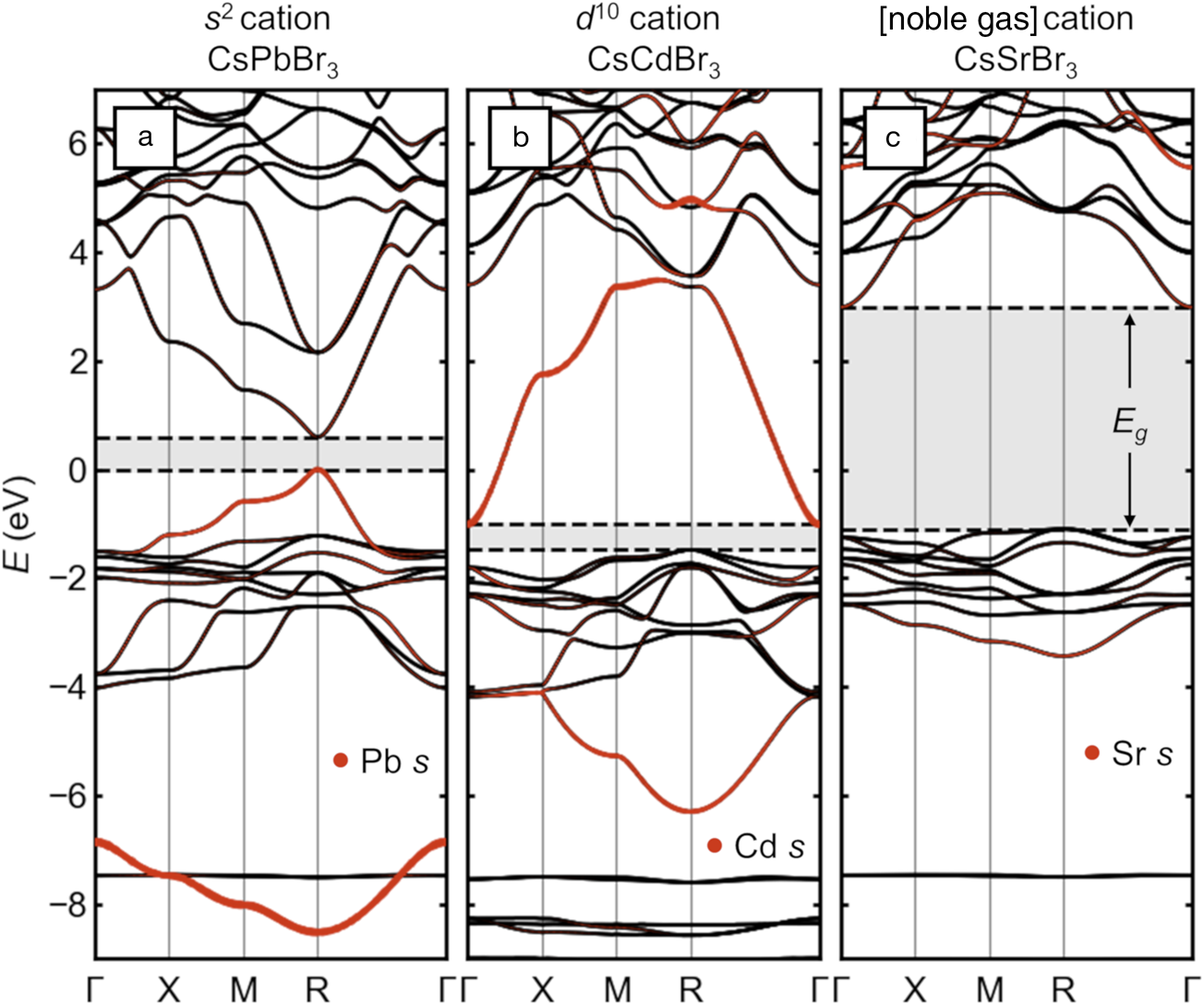
Several other studies have illustrated how decorating the perovskite lattice with s and p orbitals leads to the observed momentum-dependence of the frontier bands and location of the bandgap.Reference Huang and Lambrecht15–Reference Goesten and Hoffmann17 Rather than repeat these arguments, we show directly via ab initio calculations based on density functional theory (DFT) in Figure 2b–c the effects on the electronic structure of halide perovskites if the lone pair cation is replaced with one lacking this electron configuration. The A-site cation (Cs) and halogen (Br) are fixed across the series, and spin–orbit coupling is included.
If a “d Reference Galy, Meunier, Andersson and Åström10” cation such as Cd2+ (lacking a lone pair) with the [Kr]4d Reference Galy, Meunier, Andersson and Åström10 electron configuration is substituted on the octahedral site, the band structure is radically altered, as shown in Figure 2b. Because of better energetic alignment, the empty Cd 5s and filled Br 4p orbital interaction is more covalent, leading to wider bandwidths for the corresponding pair of bands (orange highlighting). Crucially, the upper of these two bands is not occupied (no lone pair), so the VB (derived solely from the halogens) is now ≈1.5 eV deeper than that of CsPbBr3 and much less dispersive, suggesting heavy holes, and the bandgap has become indirect. The high curvature of the conduction band (CB) suggests light electrons. Instead of balanced, small carrier masses and a direct bandgap such as in CsPbBr3, the band structure of hypothetical “CsCdBr3” (claimed once in the perovskite structure in 1928,Reference Natta and Passerini18 but subsequently reported always in the more plausible 1D BaNiO3 structure) is analogous to that of n-type conductor BaSnO3,Reference Scanlon19 but with a narrower gap.
For CsSrBr3, as shown in Figure 2c, with the “empty shell” Sr2+ cation with the [Kr] electron configuration, the situation is taken to the extreme. The shallow 5s orbitals from highly electropositive Sr strongly reduce the covalency with the Br 4p, as seen in the narrower bandwidths and reduced Sr 5s weight in the bonding band around –3 eV. The VBM is again more than 1 eV deeper than in CsPbBr3, and the hole effective mass is large. The higher band center and reduced bandwidth of the CB from this more ionic interaction creates a wide bandgap. As such, CsSrBr3 is a colorless rare-earth ion scintillator host.
Given this limited space for chemical substitutions in “single” perovskites that maintain the favorable optoelectronic properties associated with Pb2+ and Sn2+, there has been much excitement about double perovskites with rock-salt-ordering of the octahedral cations (elpasolites) since the first reports of red Cs2AgBiBr6Reference Slavney, Hu, Lindenberg and Karunadasa20,Reference McClure, Ball, Windl and Woodward21 and the corresponding chloride.Reference McClure, Ball, Windl and Woodward21,Reference Volonakis, Filip, Haghighirad, Sakai, Wenger, Snaith and Giustino22 Expanding on a previous analysis,Reference Savory, Walsh and Scanlon16 we show here that while these compounds may be interesting for other reasons, there appear to be no practically feasible chemical substitutions that qualitatively maintain the favorable band structure of the lead and tin halide (single) perovskites. The electronic-band structures of double perovskites with various combinations of octahedral cation electron configurations are presented in Figure 3.
Electronic-band structures of rock-salt-ordered halide double perovskites (elpasolites) with different combinations of electronic configurations on the octahedral cations, presented on a common energy scale. (a) Hypothetical Cs2TlBiBr6 with s Reference Kulbak, Cahen and Hodes2 Tl+ and s Reference Kulbak, Cahen and Hodes2 Bi3+. (b) Cs2AgBiBr6 with d Reference Galy, Meunier, Andersson and Åström10 Ag+ and s Reference Kulbak, Cahen and Hodes2 Bi3+. (c) Hypothetical Cs2AgInBr6 with d Reference Galy, Meunier, Andersson and Åström10 Ag+ and d Reference Galy, Meunier, Andersson and Åström10 In3+. (d) Hypothetical Cs2KBiBr6 with [Ar] K+ and s Reference Kulbak, Cahen and Hodes2 Bi3+. (e) Hypothetical Cs2KInBr6 with [Ar] K and d Reference Galy, Meunier, Andersson and Åström10 In3+. Bandgaps are indicated with shading and dashed lines. Projected s orbital character on the octahedral cations is shown as orange and blue dots. The energy scales are aligned by the semi-core Cs 5s states (around –20 eV) and are referenced to the valence-band maximum of Cs2TlBiBr6. Note: [n.g.], noble gas electron configuration.
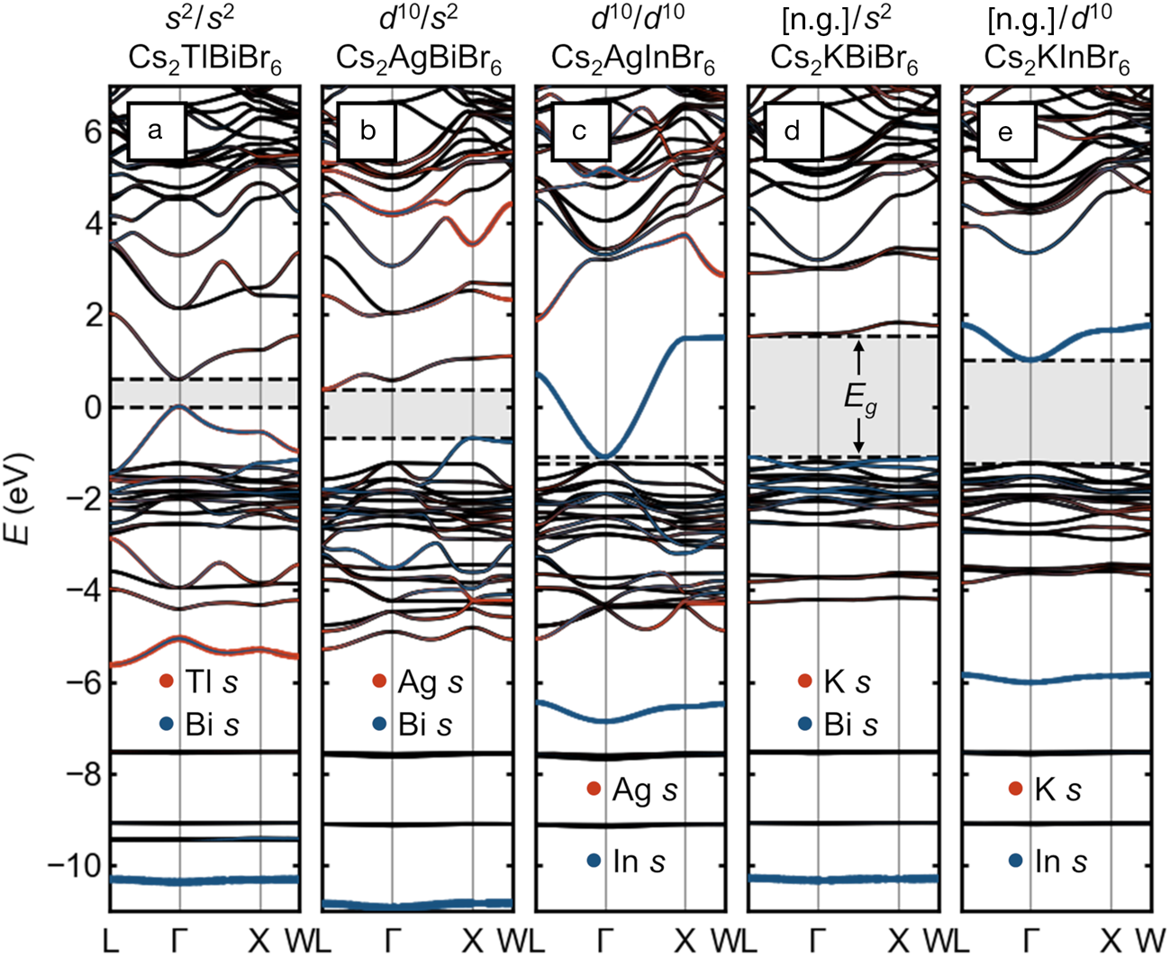
Figure 3a shows the case of the hypothetical “Cs2TlBiBr6,” with an ordering of two cations, Tl+ and Bi3+, which are isoelectronic to Pb2+. This compound thus represents only a small perturbation on CsPbBr3, and the band structure appears similar to that of CsPbBr3 simply back-folded into the FCC Brillouin zone, with a direct bandgap and a wide VB whose maximum exhibits high curvature and sits well above the (solely) Br p bands. Instead of a single bonding Pb 6s—Br 4p band centered roughly around –7.5 eV, we see two corresponding bands centered roughly around –5 eV (Tl) and –10.5 eV (Bi), reflecting the relative stability of the lone-pair s orbitals of the isolated cations, which increases in the order In+ < Tl+ < Sn2+ < Pb2+ < Sb3+ < Bi3+ < Te4+ < Po4+.Reference Stoltzfus, Woodward, Seshadri, Klepeis and Bursten23–Reference Xiao, Du, Meng, Wang, Mitzi and Yan25 While stoichiometric “Cs2TlBiBr6” has not been realized, (MA)2TlBiBr6 has been prepared, and exhibits a bandgap of ~2.2 eV.Reference Deng, Wei, Sun, Kieslich, Cheetham and Bristowe26 Unfortunately, Tl+ is exceedingly toxic (and appears too large to form a stable Cs-compound at full occupancy), and halides of In+ tend to be unstable against further oxidation or disproportionation to In0 and In3+ Reference Tuck27–Reference McCall, Friedrich, Chica, Cai, Stoumpos, Alexander, Deemyad, Wessels and Kanatzidis29 and prone to severe lone-pair-driven distortions, which reduce orbital overlap and change connectivity,Reference Lin, Chen, Gao, Cai, Jin, Etman, Kang, Lei, Lin, Folgueras, Quan, Kong, Sherburne, Asta, Sun, Toney, Wu and Yang28–Reference Tan, Stephens, Hendrickx, Hadermann, Segre, Croft, Kang, Deng, Lapidus, Kim, Jin, Kotliar and Greenblatt30 seemingly rendering halide double perovskites that are electronically equivalent to lead halide single perovskites practically out of reach.
Replacing half of the lone-pair cations with d Reference Galy, Meunier, Andersson and Åström10 cations such as Ag+ yields the now familiar case of Cs2AgBiBr6, as shown in Figure 3b. As noted previously,Reference Savory, Walsh and Scanlon16 the alternation of empty and filled s orbitals in the valence of the octahedral cations leads to a momentum dependence that moves the band edges from the zone center to two different locations on the zone boundary, resulting in an indirect gap. Though the gap remains in the visible, the VBM is significantly deeper and the hole-effective mass heavier than the all-lone-pair case. One consequence of the distinct gap nature is immediately evident in the laboratory: Powders of CsPbBr3 are a brilliant luminescent orange, whereas those of Cs2AgBiBr6 are a much duller red.
The direct bandgap is recovered when the remaining lone-pair cation is replaced with another d Reference Galy, Meunier, Andersson and Åström10 cation, as in the case of “Cs2AgInBr6,” shown in Figure 3c. However, similar to the case of “CsCdBr3,” the VB derives primarily from the anions and lies quite deep in energy and has negligible dispersion along Γ–X, suggesting poor hole transport and unfavorable band alignment. The recovery of the direct bandgap by matching the orbital angular momentum of the frontier orbitals of the octahedral cations is illustrated in the alloying of Cs2AgSb1-xInxCl6.Reference Thao Tran, Panella, Chamorro, Morey and McQueen31 While it appears “Cs2AgInBr6” has not been successfully prepared as a double perovskite, Cs2AgInCl6 has been prepared and has a wide gap of 3.3 eV.Reference Volonakis, Haghighirad, Milot, Sio, Filip, Wenger, Johnston, Herz, Snaith and Giustino32
As shown in Figure 3d–e, substituting an empty shell cation such as K+ (with the [Ar] electron configuration) in “Cs2KBiBr6” uniformly produces deep VBMs, heavy holes, and wide bandgaps (e.g., (MA)2KBiCl6 has been prepared and exhibits a gap of ~3.0 eVReference Wei, Deng, Sun, Xie, Kieslich, Evans, Carpenter, Bristowe and Cheetham33). The gap when the other cation is d Reference Galy, Meunier, Andersson and Åström10 like In3+ is somewhat narrower, but has significantly heavier electron mass than if both cations share this configuration. We note for completeness that other configurations are possible, for instance with rare-earth cations, but thus far, these appear to lead to compounds which are colorless.Reference Deng, Wie, Brivio, Wu, Sun, Bristowe and Cheetham34 These examples illustrate that uninterrupted main-group metal–halogen–main-group metal connectivity is also essential: When the connectivity is interrupted by electropositive alkali cations or by vacancies, the favorable wide valence bandwidth and the attendant band alignment and hole mass is lost. This can be seen as well in the flatter VBs and lower and deeper VBMs in low-dimensional compounds, such as PbI2,Reference Brgoch, Lehner, Chabinyc and Seshadri35 BiI3,Reference Lehner, Wang, Fabini, Liman, Hébert, Perry, Wang, Bazan, Chabinyc and Seshadri36 and ternary (chalco)halides of Sb and Bi.Reference Saparov, Hong, Sun, Duan, Meng, Cameron, Hill, Yan and Mitzi37–Reference Brandt, Poindexter, Gorai, Kurchin, Hoye, Nienhaus, Wilson, Polizzotti, Sereika, Zaltauskas, Lee, MacManus-Driscoll, Bawendi, Stevanovic and Buonassisi39
Consistently, mismatch of the angular momentum of the frontier orbitals between the two octahedral cations gives an indirect bandgap, and the only combinations aside from the practically unfeasible (In,Tl)+/(Sb,Bi)3+, which match the frontier orbitals and maintain a direct gap (e.g., Ag+/In3+), suffer from deep VBMs and heavy holes and have not been successfully prepared for the heavier halogens. Therefore, the lone pair is essential for favorable band alignment, wide VB width, and light hole effective masses.
Thus far, other materials reproducing this qualitative electronic structure (but with wider bandgaps than the known IV–VI semiconductors) have eluded discovery, but such compounds, with heavy lone-pair cations in high symmetry coordination, moderately electronegative anions, and a high dimensionality of connectivity,Reference Xiao, Meng, Wang, Mitzi and Yan40 may yet be realized. In searching for such low-cost, defect-tolerant semiconductors beyond the perovskite structure, it is worth addressing how the energy of the lone-pair orbitals varies with chemistry. Pb2+ seems to exhibit a favorable compromise between stability and covalency (as noted previously, the energy of the lone-pair s orbital increases left-to-right and top-to-bottom of the heavy main group.Reference Stoltzfus, Woodward, Seshadri, Klepeis and Bursten23–Reference Xiao, Du, Meng, Wang, Mitzi and Yan25 In+ adopts severely distorted coordination environments, which reduce orbital overlap and alter connectivity, Tl+ is too toxic, and (meta)stable halides of Sn2+ in high symmetry coordination tend to display high concentrations of compensating defects because of their high energy VBM. On the other hand, halides, oxyhalides, and chalcohalides of Bi3+ are quite stable, but the more contracted lone pair and lower symmetry coordination environments lead to narrower VBs, deeper VBM, and heavier holes.Reference Lehner, Wang, Fabini, Liman, Hébert, Perry, Wang, Bazan, Chabinyc and Seshadri36–Reference Lehner, Fabini, Evans, Hébert, Smock, Hu, Wang, Zwanziger, Chabinyc and Seshadri38 Based on this compromise, new compounds with Sb3+ in high-symmetry coordination (akin to octahedral Pb2+ in halide perovskites or cuboctahedral Tl+ in rock-salt halides) and a high degree of connectivity are ripe for exploration.
Unconventional bandgap and defect tolerance
The lone-pair electron configuration causes an antibonding VB edge, which may aid in defect tolerance. In group IV and III–V semiconductors, the VB edge is bonding in character, and the CB edge is antibonding, and for most such compounds, the band extrema are both located at the Γ point of the Brillouin zone. The situation at the VB edge is reversed in many Cu+ and Ag+-containing compounds (e.g., chalcopyrite), where the filled d-shell is shallow enough in energy to interact with the anion p orbitals, pushing up the VB edge. This is precisely what occurs in lead and tin halide perovskites but because of the filled cation s orbitals (the lone pair) rather than the d orbitals, which are too deep in energy for these cations. This unusual electronic bandgap formed between an antibonding VB (metal s—halogen p) and an antibonding CB (metal p—halogen p) is exemplified by the electronic density of states, crystal orbital Hamilton population (COHP, which provides an energy-resolved view of chemical bonding),Reference Maintz, Deringer, Tchougreeff and Dronskowski41 and schematic bonding diagram for cubic CsPbBr3 in Figure 4, shown here without spin–orbit coupling. The primary contribution from Pb 6s is in the bonding band with Br 4p around –8 eV, but the corresponding antibonding interaction produces the broad VB. The antibonding character of the VBM and the symmetry of the constituent orbitals ensures that this will occur away from the Γ point of the Brillouin zone. Though the CB is often erroneously labeled “nonbonding,” it derives from an antibonding interaction between Pb 6p and the halogens, as seen from the COHP in Figure 4 or from bandwidths in sublattice calculations.Reference Goesten and Hoffmann17 Goesten and HoffmannReference Goesten and Hoffmann17 give an excellent pedagogical discussion of the bonding in these compounds.
Orbital-projected electronic density of states (DOS), crystal orbital Hamilton population (COHP) for lead–halogen interactions, and schematic band diagram for cubic CsPbBr3. Pb 6s contributions are indicated with orange arrows. Positive values of –COHP (to the right) are bonding, and negative values are antibonding. Both the valence-band maximum and the conduction-band minimum are seen to be antibonding, with consequences for defect energetics and temperature coefficient of the bandgap. Schematic bands are colored by the dominant orbital contribution following the colors in the DOS.
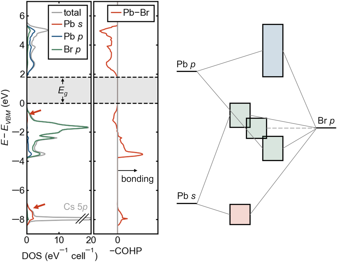
In the context of Cu+ compounds, an antibonding VB edge has been proposed to lead to shallow defects,Reference Zakutayev, Caskey, Fioretti, Ginley, Vidal, Stevanovic, Tea and Lany42 and this feature may be responsible for the shallow acceptors observed in lead halide perovskites. Because defect states would derive from atomic levels well below the VBM (e.g., Pb s and Br p in Figure 4), they would tend to form states close to the band edge or even resonant within the VB rather than deep, midgap states.Reference Yin, Shi and Yan43,Reference Brandt, Stevanovic, Ginley and Buonassisi44 Naturally, this argument does not extend directly to the (also) antibonding CB. Deep donors could form on the basis of the low-lying position of the Br p orbitals.
The relationship between chemistry, structural disorder, and electronic disorder in these compounds remains enigmatic, but this unusual antibonding VB may contribute to the defect tolerance, together with other factors such as compensatory ionic disorderReference Walsh, Scanlon, Chen, Gong and Wei45 and lattice dynamical suppression of long-range correlations in the disorder potential.Reference Gehrmann and Egger46
Unusual pressure- and temperature-dependence of the bandgap
Another consequence of these antibonding VBs and CBs is that the signs of  ${{\partial E_g} \over {\partial T}}$ and ${{\partial E_g} \over {\partial P}}$ (via the associated deformation potentials) are opposite to those in most semiconductors—the bandgaps widen with rising temperature and narrow with pressure within one structural phase. This behavior with pressure was observed decades ago in germanium chlorides and bromides,Reference Schwarz, Wagner, Syassen and Hillebrecht47 and the behavior with temperature was observed more recently in CsSnI3Reference Yu, Chen, Wang, Pfenninger, Vockic, Kenney and Shum48 and has been observed numerous times in lead and tin halide perovskites since.Reference Kontos, Kaltzoglou, Arfanis, McCall, Stoumpos, Wessels, Falaras and Kanatzidis49 Additionally, because of the large positive thermal expansion (vide infra) and small bulk moduli, these bandgap changes are quite significant. This strong temperature dependence suggests a very different temperature coefficient of performance in perovskite solar cells than their conventional cousins, although the overall effects in a single junction or tandem device are not yet known.
We have previously put forth a simple model for understanding the temperature dependence (with the same logic applying for pressure dependence) through a combination of ab initio calculations and photoluminescence measurements on CsSnBr3 as an example.Reference Fabini, Laurita, Bechtel, Stoumpos, Evans, Kontos, Raptis, Falaras, Van der Ven, Kanatzidis and Seshadri50 Because VB and CB are both antibonding, both narrow and drop with thermal expansion on warming. However, the width of the VB is more sensitive to the degree of spatial overlap, so the net result is a widening of the bandgap. Beyond these dominant volume effects, nonlinearities in the observed bandgap temperature dependences suggest an additional impact from dynamic octahedral tilting and dynamic octahedral distortions.Reference Kontos, Kaltzoglou, Arfanis, McCall, Stoumpos, Wessels, Falaras and Kanatzidis49,Reference Fabini, Laurita, Bechtel, Stoumpos, Evans, Kontos, Raptis, Falaras, Van der Ven, Kanatzidis and Seshadri50 Although a fuller treatment of electron–phonon coupling is needed for quantitative agreement, this simple bonding-based picture appears to have qualitative predictive power.
Lone-pair effects on lattice dynamics: Anharmonicity and polar distortions
As discussed in the introduction, the presence of lone pairs on Pb and Sn provides a driving force for these cations to adopt distorted, acentric coordination environments, wherein the lone pair occupies space and repels the other ligands. Examining the reported crystal structure evolution of these compounds with temperature, one observes that all the Ge compounds adopt polar structures with crystallographically distorted, acentric Ge environments, whereas all the Pb compounds (except the fluorides, with strong lone-pair stereochemical activity and octahedral tilting) adopt centrosymmetric structures with nominally centric Pb coordination. The Sn compounds are intermediate, with iodides and some bromides adopting crystallographically centric Sn environments (except for CH3NH3SnBr3, which adopts the polar Pmc21 (#26) space group at intermediate temperatures and an unknown, likely triclinic, ground state structureReference Swainson, Chi, Her, Cranswick, Stephens, Winkler, Wilson and Milman51), while the chlorides and fluorides are nonperovskite salts with [SnX 3]– pyramidal anions, because of the stronger stereochemical activity of the lone pair with these harder ligands. Despite numerous reports of ferroelectricity in perovskite lead iodides and bromides (particularly CH3NH3PbI3), a preponderance of evidence suggests the bulk is centrosymmetric in these compounds,Reference Govinda, Kore, Bokdam, Mahale, Kumar, Pal, Bhattacharyya, Lahnsteiner, Kresse, Franchini, Pandey and Sarma52,Reference Frohna, Deshpande, Harter, Peng, Barker, Neaton, Louie, Bakr, Hsieh and Bernardi53 ruling out piezo-, pyro-, and ferroelectricity.
But this is only part of the story. Obscured in this average structure view are local, dynamic, polar distortions of the octahedral cation environments evident from vibrational spectroscopy,Reference Smit, Dirksen and Stufkens54 x-ray absorption spectroscopy,Reference Ishida, Maeda, Hirano, Kubozono and Furukawa55 pair distribution functions (PDFs) from total scattering,Reference Fabini, Laurita, Bechtel, Stoumpos, Evans, Kontos, Raptis, Falaras, Van der Ven, Kanatzidis and Seshadri50,Reference Worhatch, Kim, Swainson, Yonkeu and Billinge56,Reference Laurita, Fabini, Stoumpos, Kanatzidis and Seshadri57 and ab initio calculations.Reference Fabini, Laurita, Bechtel, Stoumpos, Evans, Kontos, Raptis, Falaras, Van der Ven, Kanatzidis and Seshadri50,Reference Marronnier, Lee, Geffroy, Even, Bonnassieux and Roma58–Reference Remsing and Klein60 Raman spectroscopyReference Yaffe, Guo, Tan, Egger, Hull, Stoumpos, Zheng, Heinz, Kronik, Kanatzidis, Owen, Rappe, Pimenta and Brus61 has indicated the fluid-like dynamical nature of the perovskite lattices of CsPbBr3 and MAPbBr3, part of which is accounted for by the lone-pair activity of Pb2+. The lattice dynamics seem unique to these perovskites, and although they may not promote huge carrier mobilities, they could reduce electron–hole recombination rates, prolonging excited state carrier lifetimes. Pump-probe electron total scattering studiesReference Wu, Tan, Shen, Hu, Miyata, Trinh, Li, Coffee, Liu, Egger, Makasyuk, Zheng, Fry, Robinson, Smith, Guzelturk, Karunadasa, Wang, Zhu, Kronik, Rappe and Lindenberg62 indicate significant structural distortions upon photoexcitation in several of these compounds as well, although it is unclear as of yet if these are connected to the same lone-pair-driven instability.
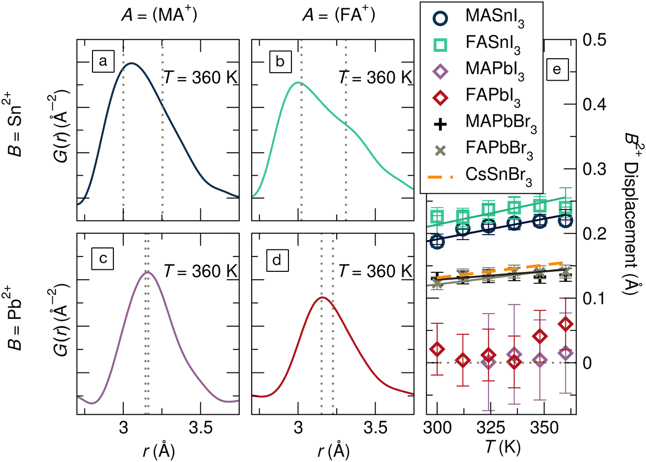
These severe local distortions are exemplified by the x-ray pair distribution functions (PDFs) for hybrid tin and lead iodide perovskites in Figure 5a–d.Reference Laurita, Fabini, Stoumpos, Kanatzidis and Seshadri57 From the crystallographically cubic structures for all four compounds at this temperature,Reference Laurita, Fabini, Stoumpos, Kanatzidis and Seshadri57 one would expect a single, symmetric peak just above r = 3 Å, reflecting a single metal–iodide bond distance. Instead, all four exhibit asymmetric peaks, from the moderately asymmetric metal–I correlation in MAPbI3 (Figure 5c) to the nearly bifurcated one in FASnI3 (Figure 5b). Modeling these PDFs (and those for hybrid lead bromides and CsSnBr3) with a small-box rhombohedral distortion, as observed crystallographically in the Ge halide perovskites, offers a simple way to understand the underlying chemical trends, as shown in Figure 5e. The magnitude of the local, polar distortions can be tuned by chemical substitution on all three sites, with lighter Sn2+, harder Br–, and larger A-site cations all enhancing this effect.Reference Laurita, Fabini, Stoumpos, Kanatzidis and Seshadri57 Indeed, these chemical rules are precisely in line with those enumerated for rock-salt chalcogenides based on ab initio studies.Reference Waghmare, Spaldin, Kandpal and Seshadri63
The x-ray pair distribution function (PDF), represented by G(r), at 360 K for (a) MASnI3, (b) FASnI3, (c) MAPbI3, (d) FAPbI3 revealing severely distorted MI6 octahedra in these crystallographically cubic phases (MA = [CH3NH3]+; FA = [CH(NH2)2]+). (e)Displacements of the octahedral cations from small-box modeling of the PDF with a rhombohedral distortion. Values for MAPbBr3, FAPbBr3, and CsSnBr3 are additionally shown. The severe asymmetry in the metal-halogen PDF peak is seen for all compounds but is strongest for tin iodides and more moderate for lead iodides. Reproduced with permission from Reference 57. © 2017 Royal Society of Chemistry.
Notably, these polar distortions are distinct from the well-known nonpolar dynamic tilting of rigid octahedra in high-temperature phases, which is driven by ionic size considerations rather than bonding and covalency and is ubiquitous in perovskites with undersized A-cations. Because of their polar nature, the lone-pair-driven distortions also impact dielectric properties (vide infra) and possibly allow for dynamic relativistic spin polarizationReference Kim, Im, Freeman, Ihm and Jin64 in these crystallographically centrosymmetric phases. Additionally, the anharmonicity associated with this bonding naturally has the effect of reducing lattice thermal conductivity, a point which has been covered extensively in the literature on thermoelectrics with lone-pair cations. Aside from the impacts on dielectric and thermomechanical properties, one expects that these unusual lattice dynamics would be linked to the electronic disorder in these structurally soft materials,Reference Egger, Bera, Cahen, Hodes, Kirchartz, Kronik, Lovrincic, Rappe, Reichman and Yaffe1,Reference Gehrmann and Egger46 which in turn dictates many excited state properties.
Large ionic dielectric response
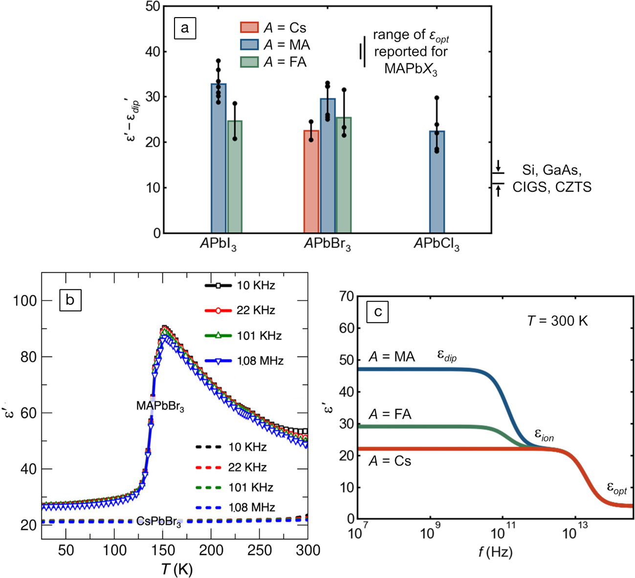
The anharmonic potential for polar octahedral distortions underlying this observed “hidden” local structure should also manifest in an elevated ionic dielectric response, independent of the reorientation of dipolar molecular cations in the hybrid compounds. This is because the nominal, crystallographic, high-symmetry coordination of the lone-pair-bearing cation is a metastable saddle point in the potential energy landscape. Accordingly, a small applied field is sufficient to induce a large dipole from the distorted, acentric coordination because of the stereochemically active lone pair. As seen in Figure 6a, all the compounds in this class which have been measured to date have low-frequency dielectric constants two to three times those of silicon, III–Vs, kesterites, and chalcopyrites, even when molecular dipole contributions are removed.Reference Govinda, Kore, Bokdam, Mahale, Kumar, Pal, Bhattacharyya, Lahnsteiner, Kresse, Franchini, Pandey and Sarma52,Reference Wilson, Frost, Wallace and Walsh65–Reference Almond and Bowen75 Without the molecular dipole contributions, the dielectric constants of the inorganic and hybrid compounds are nearly identical, as illustrated by Govinda and co-workers for the case of lead bromides in Figure 6b. The schematic frequency dependence of the dielectric function (modeled after Young and FrederikseReference Young and Frederikse76 and based off of reported molecular reorientation rates and optical phonon frequencies) is depicted in Figure 6c.
(a) Reported experimental static dielectric permittivity without molecular dipole contributions, εʹ—εdipʹ, compiled from the literature, in units of the vacuum permittivity, ε0. These values are isolated via kHz or MHz capacitance measurements in the low temperature limitReference Govinda, Kore, Bokdam, Mahale, Kumar, Pal, Bhattacharyya, Lahnsteiner, Kresse, Franchini, Pandey and Sarma52,Reference Onoda-Yamamuro, Matsuo and Suga67–Reference Fabini, Hogan, Evans, Stoumpos, Kanatzidis and Seshadri69,Reference Anusca, Balčiūnas, Gemeiner, Svirskas, Sanlialp, Lackner, Fettkenhauer, Belovickis, Samulionis, Ivanov, Dkhil, Banys, Shvartsman and Lupascu71–Reference Schueller, Laurita, Fabini, Stoumpos, Kanatzidis and Seshadri74 or at room temperature using GHz66 or THzReference Sendner, Nayak, Egger, Beck, Müller, Epding, Kowalsky, Kronik, Snaith, Pucci and Lovrincic70 radiation. Individual values (black dots) are shown, and bar height is the average value. The range of values for typical photovoltaic semiconductors is shown on the right-hand side (CIGS: Cu[In,Ga][S,Se]2; CZTS: Cu2ZnSnS4). The range of reported optical dielectric constants, εopt, for MAPb(Cl,Br,I)3 is also indicated.Reference Wilson, Frost, Wallace and Walsh65 (b) Low-frequency dielectric response of CsPbBr3 and MAPbBr3, showing that the ionic response of the two compounds is similar when reorientation of the molecular dipole is frozen out. Adapted with permission from Reference 52. © 2017 American Chemical Society. (c) Schematic of the frequency dependence of the dielectric response of halide perovskites at room temperature, illustrating static, ionic, and (sub-bandgap) optical regimes.
This elevated lattice polarizability (high static dielectric constant), because of the lone pairs, is far from a curiosity. Rather, it is the likely microscopic mechanism behind the hypothesized formation of large polarons in these materials.Reference Zhu and Podzorov77 In principle, a higher dielectric response (on the relevant time scale) should screen the Coulomb interaction between charge carriers and other carriers or charged defects, reducing scattering and recombination rates. Although focused study of the impacts of unusually strong dielectric screening on carrier transport appears to be in its infancy,Reference Du and Singh78,Reference Du79 an early result from doped ferroelectric complex oxides is quite intriguing.Reference Siemons, McGuire, Cooper, Biegalski, Ivanov, Jellison, Boatner, Sales and Christen80 In halide perovskites, there is ample circumstantial evidence, although direct proof remains challenging, as it can be difficult in practice to isolate the stimulus of interest (e.g., chemical substitution simultaneously alters the chemical bonding, ionic sizes, and defect energetics).
Notably, this phenomenon of a large ionic dielectric response should be fully general to compounds with lone-pair cations in relatively high symmetry environments (if the coordination is severely distorted, this may indicate that the double well is quite deep, akin to a polar phase whose polarization cannot be ferroelectrically switched before dielectric breakdown). An instructive example in simple binary compounds can be found in comparing PbS (in which lone-pair-driven dynamic distortions have been observedReference Božin, Malliakas, Souvatzis, Proffen, Spaldin, Kanatzidis and Billinge81) and CdS (without a lone-pair cation): PbS has a static dielectric constant more than one order of magnitude higher than that of CdS (even when accounting for the difference in optical dielectric constants from the rather different bandgaps).Reference Young and Frederikse76 Several other semiconductors with lone-pair cations have high dielectric constants, including Sb3+ sulfides and selenides, SbSI (with a ferroelectric transition around room temperature), and Tl+ halides.Reference Young and Frederikse76
Enormous positive thermal expansion
As a purely anharmonic effect, thermal expansion behavior offers another window into the unusual lattice dynamics of these compounds—though we note that this property reflects both the polar modes discussed previously and the more familiar, nonpolar anharmonic modes associated with octahedral tilting in perovskites with undersized A-cations. The experimentally reported values of the volumetric thermal expansion coefficient,  ${\rm \alpha }_{\rm V} = {1 \over V}\left({{{\partial V} \over {\partial T}}} \right)_p$, for tin and lead bromides and iodides are presented in Figure 7a (reliable figures are not yet available for FASnBr3 and most of the corresponding chlorides). Though lattice parameters can be determined to high precision, such expansion coefficients necessitate taking finite differences of volumes, amplifying greatly any systematic error in lattice parameters across studies, laboratories, and instruments. As such, in almost every instance, lattice parameters at different temperatures have been taken from the same publication. Additionally, the volumetric thermal expansion of these materials seems generally not to be linear over wide temperature ranges,Reference Fabini, Laurita, Bechtel, Stoumpos, Evans, Kontos, Raptis, Falaras, Van der Ven, Kanatzidis and Seshadri50,Reference Fabini, Stoumpos, Laurita, Kaltzoglou, Kontos, Falaras, Kanatzidis and Seshadri88 even at temperatures well above any quantum effects, so αV has been computed near room temperature whenever possible. Values derived from neutron diffraction, or older values that deviate significantly from those based on modern diffractometers, have been excluded.
(a) Volumetric thermal expansion coefficients, αV, of perovskite tin and lead bromides and iodides compiled from the literature.Reference Fabini, Laurita, Bechtel, Stoumpos, Evans, Kontos, Raptis, Falaras, Van der Ven, Kanatzidis and Seshadri50,Reference Worhatch, Kim, Swainson, Yonkeu and Billinge56,Reference Schueller, Laurita, Fabini, Stoumpos, Kanatzidis and Seshadri74,Reference Chung, Song, Im, Androulakis, Malliakas, Li, Freeman, Kenney and Kanatzidis82–Reference Fabini, Stoumpos, Laurita, Kaltzoglou, Kontos, Falaras, Kanatzidis and Seshadri88 Where multiple reliable values are available (e.g., different temperature ranges), individual points and the corresponding range are shown, and the bar height is the average value. The value for c-Si is shown for comparison. (b) Schematic μ–t phase space (μ = octahedral factor; t = tolerance factor) illustrating the purely geometric effects of chemical substitution on each of the three sites.
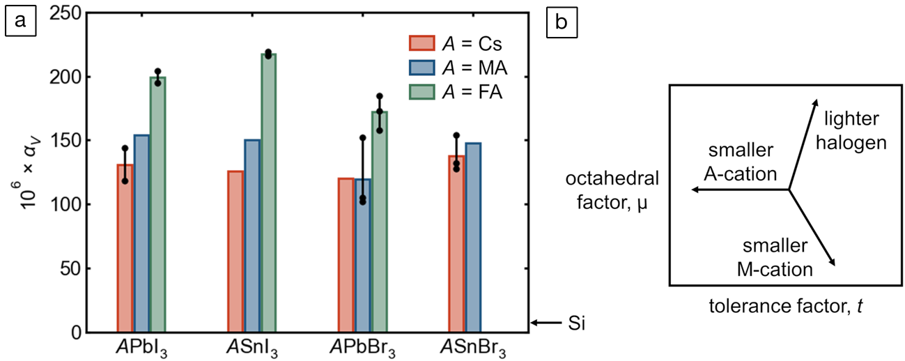
Several features are evident from Figure 7. Most glaringly, across all the iodides and bromides of tin and lead, the coefficients of volumetric thermal expansion are extremely large, more than one order of magnitude larger than that of c-Si (~8 × 10⁶).Reference Becker, Seyfried and Siegert89 As noted in previous reports from the authors, αV for FAPbI3 and FASnI3 appear to be the largest values known for any 3D-extended crystalline solids near room temperatureReference Schueller, Laurita, Fabini, Stoumpos, Kanatzidis and Seshadri74,Reference Fabini, Stoumpos, Laurita, Kaltzoglou, Kontos, Falaras, Kanatzidis and Seshadri88 (at least one framework cyanide, and likely other compounds, appear to have a larger value at low temperaturesReference Goodwin, Calleja, Conterio, Dove, Evans, Keen, Peters and Tucker90). Although this is remarkable from a fundamental perspective, this suggests significant challenges in applications, such as the possibility of fatigue cracking or substrate delamination because of diurnal temperature cycling in solar cells—though the “soft” kinetics of these materials and the corresponding high homologous temperatures may in fact allow self-healing.
Strikingly, in most cases, values of αV of the tin halides appear to be comparable to or even somewhat higher than those of the corresponding lead halides. This includes the case of FASnI3 and FAPbI3, for which values are reported by the same group at comparable temperatures based on measurements at the same high-resolution synchrotron diffractometer.Reference Schueller, Laurita, Fabini, Stoumpos, Kanatzidis and Seshadri74,Reference Fabini, Stoumpos, Laurita, Kaltzoglou, Kontos, Falaras, Kanatzidis and Seshadri88 This is striking for two reasons. First, one typically expects “stiffening” of (thermo)mechanical properties as one ascends a group in the periodic table, such as higher bulk moduli and higher Debye temperatures (though we must not conflate stiffer harmonicity with reduced anharmonicity). Second, substituting tin for lead corresponds to a smaller octahedral factor and a larger tolerance factor (illustrated in Figure 7b)—the latter implying that tilting anharmonicity is reduced in making this substitution. Even in the face of a lighter divalent cation and lesser octahedral tilting (and lesser anharmonicity of those modes), tin halides have greater coefficients of thermal expansion, suggesting extreme anharmonicity of the Sn–X bond.
This is in line with the expectations based on lone-pair stereochemistry and the acute local distortions observed in tin halides by x-ray PDF discussed previously. We note, however, that at this time, one cannot rule out the possibility that a higher tolerance factor suppresses a negative contribution from rigid octahedral rocking modes as observed in ScF3 and ReO3—the nonlinear temperature-dependence of αV through tilting phase transitions observed in CsSnBr3Reference Fabini, Laurita, Bechtel, Stoumpos, Evans, Kontos, Raptis, Falaras, Van der Ven, Kanatzidis and Seshadri50 and FAPbI3Reference Fabini, Stoumpos, Laurita, Kaltzoglou, Kontos, Falaras, Kanatzidis and Seshadri88 indicates this is a possibility. The lone pair (in part) causes these materials to have among the highest thermal expansion coefficients known for 3D-bonded extended solids.
Summary
The electronic configuration of Pb (Sn) in halide perovskites––with a 6s Reference Kulbak, Cahen and Hodes2 (5s Reference Kulbak, Cahen and Hodes2) lone pair––imparts several unusual properties to these compounds, many of which are favorable for their optoelectronic applications. Via its interaction with the anions, the lone pair directly produces a wide VB, suitable band alignments for the absorption of visible light and the injection of carriers to common hole transport layers, and a light effective mass for holes. The antibonding nature of states at the VB edge may contribute to the defect tolerance of these materials and produces a large positive (negative) bandgap temperature (pressure) coefficient. The lattice dynamics are also profoundly affected: The tendency for the lone pair to express its stereochemistry and “take up space” produces a highly anharmonic energy landscape for polar distortions of the octahedral cation environments. This, in turn, results in crystallographically hidden, local distortions, enhanced dynamic behavior, elevated ionic dielectric response, reduced lattice thermal conductivity, and (in part) to positive thermal expansion that is among the largest known for 3D extended solids.
While the trajectory of solar-cell performance based on lead halide perovskites in the last decade has been remarkable, practical challenges for widespread adoption and the possibility of other uses motivate the continued and expanded exploration of applications beyond photovoltaics. These include those in light emission and detection, quantum behavior, thermoelectrics, photocatalysis, and devices that couple charge and spin in relativistic, noncentrosymmetric systems.
Equipped with these chemical insights into the myriad effects of lone pairs coupled with the wealth of predictions from recent computer-aided materials discovery efforts,Reference Brandt, Stevanovic, Ginley and Buonassisi44,Reference Kuhar, Pandey, Thygesen and Jacobsen91–Reference Jin, Zhang, Li, Wang, Wan, Guo and Wei93 there is an opportunity for materials scientists and inorganic chemists to fill in the gaps in the existing phase diagrams of pnictides, chalcogenides, halides, and mixed-anion systems of the heavy main group. Similarly remarkable new semiconductors may yet be found.
Acknowledgments
This work was supported by the US Department of Energy, Office of Science, Basic Energy Sciences, under Grant No. SC0012541. D.H.F. gratefully acknowledges financial support from the Alexander von Humboldt Foundation.
 Douglas H. Fabini is an Alexander von Humboldt Postdoctoral Fellow at the Max Planck Institute for Solid State Research in Stuttgart, Germany. He received his PhD degree in materials from the University of California, Santa Barbara, in 2018, and his BS degree in mechanical engineering from the University of California, Berkeley, in 2011. His research interests include the structure and dynamics of hybrid organic–inorganic materials and computer-aided discovery of high-performance functional inorganic materials. Fabini can be reached by email at d.fabini@fkf.mpg.de.
 Ram Seshadri is the Fred and Linda R. Wudl Professor of Materials Science, in the Materials Department and the Department of Chemistry and Biochemistry at the University of California, Santa Barbara. He is also the director of the National Science Foundation Materials Research Science and Engineering Centers site, the Materials Research Laboratory. His research group investigates structure–property relations in functional materials, and he has studied the chemistry and function of lone pairs in the solid state for at least two decades. He is a Fellow of the Royal Society of Chemistry, the American Physical Society, and the American Association for the Advancement of Science. Seshadri can be reached by email at seshadri@mrl.ucsb.edu.
 Mercouri G. Kanatzidis is a Charles E. and Emma H. Morrison Professor of Chemistry at Northwestern University. He has been named a Presidential Young Investigator by the National Science Foundation, an Alfred P. Sloan Fellow, a Beckman Young Investigator, a Camille and Henry Dreyfus Teaching Scholar, a Royal Society of Chemistry Fellow, and a Guggenheim Fellow. His awards include the Einstein Professor Award, Chinese Academy of Sciences, the International Thermoelectric Society Outstanding Achievement Award, the MRS Medal (2014), the ENI Award for the “Renewable Energy Prize,” the Royal Chemical Society's de Gennes Prize (2015), the American Institute of Chemists Chemical Pioneer Award (2018), and the DOE Ten at Ten Scientific Ideas Award for the first demonstration of all-solid-state solar cells using halide perovskite materials (2019). Kanatzidis can be reached by email at m-kanatzidis@northwestern.edu.


 Open access