


1 Introduction
Established high-power Ti:sapphire laser systems[ Reference Jeong and Lee 1 – Reference Wang, Wang, Rockwood, Luther, Hollinger, Curtis, Calvi, Menoni and Rocca 9 ] are able to deliver laser pulses up to several PW at a high repetition rate of 0.05–1 Hz. Focusing them to relativistic intensities allows one to create laser-driven secondary sources in a wide range from ionizing radiation[ Reference Daido, Nishiuchi and Pirozhkov 10 – Reference Norreys, Santala, Clark, Zepf, Watts, Beg, Krushelnick, Tatarakis, Dangor, Fang, Graham, McCanny, Singhal, Ledingham, Creswell, Sanderson, Magill, Machacek, Wark, Allott, Kennedy and Neely 13 ] to extreme ultraviolet (XUV) and THz pulses[ Reference Lichters, Meyer-ter-Vehn and Pukhov 14 – Reference Bleko, Karataev, Konkov, Kruchinin, Naumenko, Potylitsyn and Vaughan 17 ]. Solid-density metal targets are being used to create ion sources[ Reference Bin, Obst-Huebl, Mao, Nakamura, Geulig, Chang, Ji, He, De Chant, Kober, Gonsalves, Bulanov, Celniker, Schroeder, Geddes, Esarey, Simmons, Schenkel, Blakely, Steinke and Snijders 18 , Reference Xu, Streeter, Ettlinger, Ahmed, Astbury, Borghesi, Bourgeois, Curry, Dann, Dover, Dzelzainis, Istokskaia, Gauthier, Giuffrida, Glenn, Glenzer, Gray, Green, Hicks, Hyland, King, Loughran, Margarone, McCusker, McKenna, Parisuaña, Parsons, Spindloe, Symes, Treffert, Palmer and Najmudin 19 ], flashes of highly energetic X-rays[ Reference Haney, Berger, Kubiak, Rockett and Hunter 20 , Reference Jiang, Lee, Li, Ketwaroo and Rose-Petruck 21 ] and XUV light sources[ Reference Fujioka, Nishimura, Nishihara, Miyanaga, Izawa, Mima, Shimada and Sunahara 22 ]. A high-repetition-rate operation is important for many applications in medicine and fusion science[ Reference Roth, Cowan, Key, Hatchett, Brown, Fountain, Johnson, Pennington, Snavely, Wilks, Yasuike, Ruhl, Pegoraro, Bulanov, Campbell, Perry and Powell 23 , Reference Ledingham, McKenna, McCanny, Shimizu, Yang, Robson, Zweit, Gillies, Bailey, Chimon, Clarke, Neely, Norreys, Collier, Singhal, Wei, Mangles, Nilson, Krushelnick and Zepf 24 ], but poses a challenge for system integrity.
Debris management is an important aspect of ultrahigh-intensity laser–solid interaction at a high repetition rate. The amount of ejected mass is of the order of hundreds of μg per laser shot[ Reference Andrew and Wallace 25 , Reference Ehret, Apiñaniz, Henares, Lera, de Luis, Pérez-Hernández, Volpe and Gatti 26 ] and the deposition of the ablated material is observed to deteriorate beamline components[ Reference Fujioka, Nishimura, Nishihara, Miyanaga, Izawa, Mima, Shimada and Sunahara 22 , Reference Andrew and Wallace 25 , Reference Booth, Astbury, Bryce, Clarke, Gregory, Green, Haddock, Heathcote and Spindloe 27 ]. Available detailed characterizations of debris have been limited to non-relativistic laser intensities just above the ionization threshold[ Reference Fujioka, Nishimura, Nishihara, Miyanaga, Izawa, Mima, Shimada and Sunahara 22 , Reference Ando, Fujioka, Shimada, Birou, Maeda, Yasuda, Nagai, Norimatsu, Nishimura, Nishihara, Miyanaga, Izawa and Mima 28 , Reference Amano, Inaoka, Hiraishi, Miyamoto and Mochizuki 29 ] and high-energy long-pulse lasers[ Reference Andrew, Chevalier, Egan, Geille, Jadaud, Quessada, Raffestin, Rubery, Treadwell and Videau 30 ]. First characterization attempts for relativistic high-power laser interactions show a timeline of small debris particles ejected earlier, with a fast ejection speed, and successively larger projectiles with lower velocity[ Reference Booth, Astbury, Bryce, Clarke, Gregory, Green, Haddock, Heathcote and Spindloe 27 ]. These studies further indicate an asymmetry of ejection early on, with more debris being ejected away from the side on which the laser interaction takes place, but lack a characterization of the spatially resolved debris deposition.
This paper presents a characterization of ejected debris with spatial resolution, for the first time, that will allow an evaluation of mitigation strategies to avoid damage and deterioration of beamline components, diagnostics and metrology devices.
The paper is structured as follows: (i) after a brief introduction of the novel methodology that is used to derive spatially resolved measurements from flatbed scans in Section 2, (ii) we present results from an experimental campaign at a high-power laser in Section 3 that shows two distinct types of debris, and (iii) close with the discussion and conclusion in Sections 4 and 5, respectively, evaluating the amount of ejected debris, relating results to an available model.
2 Materials and methods
Experiments for this work are conducted at the Extreme Light Infrastructure Nuclear Physics (ELI-NP) facility[
Reference Doria, Cernaianu, Ghenuche, Stutman, Tanaka, Ticos and Ur
31
] with a high-power 1 PW Ti:sapphire laser delivering on target ${E}_{\mathrm{L}}\approx 22\;\mathrm{J}$
within a pulse duration of
${E}_{\mathrm{L}}\approx 22\;\mathrm{J}$
within a pulse duration of ${\tau}_{\mathrm{L}}\approx 30\;\mathrm{fs}$
(giving a total power on target of
${\tau}_{\mathrm{L}}\approx 30\;\mathrm{fs}$
(giving a total power on target of $\approx 0.7\;\mathrm{PW}$
). The energy is extrapolated from calibrations recorded at low energy and the pulse duration is measured on-shot with a frequency-resolved optical gating (FROG) system that diagnoses a picked-up reflection from a small elliptical mirror positioned before the focusing parabola. The laser pulse is focused with an incidence angle of 45° onto
$\approx 0.7\;\mathrm{PW}$
). The energy is extrapolated from calibrations recorded at low energy and the pulse duration is measured on-shot with a frequency-resolved optical gating (FROG) system that diagnoses a picked-up reflection from a small elliptical mirror positioned before the focusing parabola. The laser pulse is focused with an incidence angle of 45° onto $\left(50\pm 5\right)\;\mu \mathrm{m}$
thick nickel disk targets, with a focal spot diameter of
$\left(50\pm 5\right)\;\mu \mathrm{m}$
thick nickel disk targets, with a focal spot diameter of ${d}_{\mathrm{L}}\approx 4\;\mu \mathrm{m}$
full width at half-maximum (FWHM). The focal spot at high energy is estimated to be the same as for low-energy measurements[
Reference Danson, Brummitt, Clarke, Collier, Fell, Frackiewicz, Hancock, Hawkes, Hernandez-Gomez, Holligan, Hutchinson, Kidd, Lester, Musgrave, Neely, Neville, Norreys, Pepler, Reason, Shaikh, Winstone, Wyatt and Wyborn
32
], even if the Strehl ratio might be different[
Reference Bromage, Bahk, Irwin, Kwiatkowski, Pruyne, Millecchia, Moore and Zuegel
33
,
Reference Pirozhkov, Fukuda, Nishiuchi, Kiriyama, Sagisaka, Ogura, Mori, Kishimoto, Sakaki, Dover, Kondo, Nakanii, Huang, Kanasaki, Kondo and Kando
34
]. The setup is shown in Figure 1, with the focusing parabola (off-axis parabola (OAP)) in the back and targets mounted on a wheel.
${d}_{\mathrm{L}}\approx 4\;\mu \mathrm{m}$
full width at half-maximum (FWHM). The focal spot at high energy is estimated to be the same as for low-energy measurements[
Reference Danson, Brummitt, Clarke, Collier, Fell, Frackiewicz, Hancock, Hawkes, Hernandez-Gomez, Holligan, Hutchinson, Kidd, Lester, Musgrave, Neely, Neville, Norreys, Pepler, Reason, Shaikh, Winstone, Wyatt and Wyborn
32
], even if the Strehl ratio might be different[
Reference Bromage, Bahk, Irwin, Kwiatkowski, Pruyne, Millecchia, Moore and Zuegel
33
,
Reference Pirozhkov, Fukuda, Nishiuchi, Kiriyama, Sagisaka, Ogura, Mori, Kishimoto, Sakaki, Dover, Kondo, Nakanii, Huang, Kanasaki, Kondo and Kando
34
]. The setup is shown in Figure 1, with the focusing parabola (off-axis parabola (OAP)) in the back and targets mounted on a wheel.
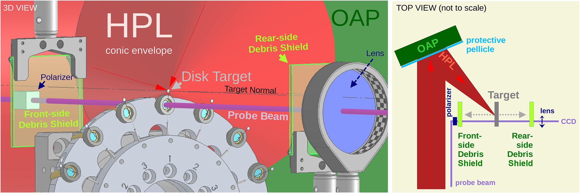
Figure 1 Two sputter plates from fused silica are used to shield probe beam optics from debris in solid-target experiments at the ELI-NP high-power laser (HPL) facility. Note that the laser is focused to relativistic intensities via an off-axis parabola (OAP) onto a disk target, which is protected against debris by a thin pellicle. The front-side debris shield protects a polarizer aimed towards the target normal on the laser-interaction side of a disk target; the rear-side debris shield catches debris in front of an imaging lens. The target normal is collinear with the normal of both debris shields.
Two 1 mm thick and $50\;\mathrm{mm}\times 50\;\mathrm{mm}$
squared sputter plates produced from fused silica (FS) are used to catch debris that is emitted away from the respective target front and rear sides. The plates were originally meant for another scope, solely to protect the optics of a probe beam setup (not further discussed hereinafter). The front-sided sputter plate is placed in front of a polarizer facing the laser-interaction side, while the rear-sided sputter plate is placed in front of an imaging lens. Note the auxiliary character of this arrangement of catchers, as the OAP is by default protected with a thin pellicle. The plates’ centres are not perfectly collinear with the laser-interaction point, but shifted by 3 mm down with respect to the target, and their surfaces are parallel to the target surface. The distance of the rear plate to the interaction point is
$50\;\mathrm{mm}\times 50\;\mathrm{mm}$
squared sputter plates produced from fused silica (FS) are used to catch debris that is emitted away from the respective target front and rear sides. The plates were originally meant for another scope, solely to protect the optics of a probe beam setup (not further discussed hereinafter). The front-sided sputter plate is placed in front of a polarizer facing the laser-interaction side, while the rear-sided sputter plate is placed in front of an imaging lens. Note the auxiliary character of this arrangement of catchers, as the OAP is by default protected with a thin pellicle. The plates’ centres are not perfectly collinear with the laser-interaction point, but shifted by 3 mm down with respect to the target, and their surfaces are parallel to the target surface. The distance of the rear plate to the interaction point is $\left(125\pm 5\right)\;\mathrm{mm}$
, while the front plate is positioned at
$\left(125\pm 5\right)\;\mathrm{mm}$
, while the front plate is positioned at $\left(95\pm 10\right)\;\mathrm{mm}$
.
$\left(95\pm 10\right)\;\mathrm{mm}$
.
After the experiment, the sputter plates are scanned with an EPSON V-750-PRO flatbed scanner to obtain the spatially resolved deposited debris thickness ${z}_{\mathrm{Ni}}$
as a function of the transmittance
${z}_{\mathrm{Ni}}$
as a function of the transmittance $T={I}_{\mathrm{t}}/{I}_0$
. Here,
$T={I}_{\mathrm{t}}/{I}_0$
. Here, ${I}_0$
is the intensity of the incident wave and
${I}_0$
is the intensity of the incident wave and ${I}_{\mathrm{t}}$
the intensity at the exit of the double-layer system. The details of the scanning procedure are outlined in Appendix A and the calculation of the transmission of a flat double-layer system is revisited in Appendix B. The theoretically predicted transmittance of evaporated nickel deposit is shown in Figure 2 as a function of the layer thickness for three channels of a colour scan. One notes the good agreement between the different colour channels, which points to a flat spectral response.
${I}_{\mathrm{t}}$
the intensity at the exit of the double-layer system. The details of the scanning procedure are outlined in Appendix A and the calculation of the transmission of a flat double-layer system is revisited in Appendix B. The theoretically predicted transmittance of evaporated nickel deposit is shown in Figure 2 as a function of the layer thickness for three channels of a colour scan. One notes the good agreement between the different colour channels, which points to a flat spectral response.
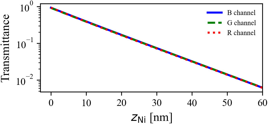
Figure 2 Predicted transmittance through nickel deposit of thickness ${z}_{\mathrm{Ni}}$
on a 1 mm thick silica plate for three channels of an RGB scan with the EPSON V-750-PRO flatbed scanner.
${z}_{\mathrm{Ni}}$
on a 1 mm thick silica plate for three channels of an RGB scan with the EPSON V-750-PRO flatbed scanner.
3 Results
Raw scans of debris collected on the sputter plates are shown in Figure 3, with both plates having recessed areas that were protected from debris by mounting structures. Different interference patterns can be observed in Figures 3(a) and 3(b), which stem from the slightly different thicknesses of the silica plate. However, their influence on the scanned intensity is smaller than the error bars of the measurements performed. Debris originates from three laser shots, two shots on targets with diameter ${d}_{\mathrm{t}}=0.5\;\mathrm{mm}$
and one shot on a disk of 2 mm diameter. The sputter plates are coated by a surfacic deposition of debris, a weak but distinct areal deposition that uniformizes towards the edges of the plates. The uniformity of the deposition can be observed in contrast to the protected area by the sputter plate’s holders (white area in Figure 3).
${d}_{\mathrm{t}}=0.5\;\mathrm{mm}$
and one shot on a disk of 2 mm diameter. The sputter plates are coated by a surfacic deposition of debris, a weak but distinct areal deposition that uniformizes towards the edges of the plates. The uniformity of the deposition can be observed in contrast to the protected area by the sputter plate’s holders (white area in Figure 3).
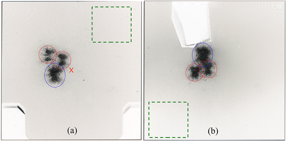
Figure 3 Debris deposited on silica plates positioned in the target normal direction (a) atop the target rear, and (b) atop the target front side facing the high-power laser at the ELI-NP 1 PW facility. Elliptical dashed lines mark areas of a rough surface and the dashed squares indicate ROIs where the debris deposition is uniform. The silica plates are 50 mm squares; visible blank areas stem from mounting clamps used for positioning the plates.
In addition, three distinct marks are observed towards the target normal (highlighted with elliptical dashed lines). Slight target misalignment of less than 5° might be responsible for the spatial separation of the marks. This hypothesis is supported by the diametrical opposition of structurally similar marks with respect to the target position. Further, one notes that two small marks (highlighted with red dashed lines) contrast one large mark (highlighted with blue dashed lines) and it is reasonable to assume that small marks correspond to shots on small disk targets. A detailed characterization of the marks is done using white-light interferometry, profilometry and a scanning electron microscope (SEM), as shown in Figure 4 and available as dataset[
Reference Haddock, Astbury, Vladisavlevici, Ehret and Bradford
35
]. The surface characteristics change abruptly from uniform deposition outside the marks to a complex ablation–redeposition pattern, likely to be mechanical damage. Ablation craters reach depths of several tens of μm and diameters of hundreds of μm. The average depth is $10\;\mu \mathrm{m}$
(as measured with the profilometer) and the ablated volume within the marks amounts to
$10\;\mu \mathrm{m}$
(as measured with the profilometer) and the ablated volume within the marks amounts to $\approx 0.0231\;{\mathrm{mm}}^3$
atop the target front side and
$\approx 0.0231\;{\mathrm{mm}}^3$
atop the target front side and $\approx 0.0095\;{\mathrm{mm}}^3$
atop the target rear side (as deduced from white-light interferometry). With a glass density of
$\approx 0.0095\;{\mathrm{mm}}^3$
atop the target rear side (as deduced from white-light interferometry). With a glass density of $5\;\mathrm{g}\;{\mathrm{cm}}^{-3}$
, the mass of ablated material from the FS plates is
$5\;\mathrm{g}\;{\mathrm{cm}}^{-3}$
, the mass of ablated material from the FS plates is $\approx 115\;\mu \mathrm{g}$
atop the target front side and
$\approx 115\;\mu \mathrm{g}$
atop the target front side and $\approx 47\;\mu \mathrm{g}$
atop the target rear side. An additional element analysis via energy-dispersive X-ray spectroscopy (EDS) in an SEM reveals the atomic composition of the surfacing layer of the sample:
$\approx 47\;\mu \mathrm{g}$
atop the target rear side. An additional element analysis via energy-dispersive X-ray spectroscopy (EDS) in an SEM reveals the atomic composition of the surfacing layer of the sample: $\left(36.1\pm 0.4\right)\%$
Ni deposition and
$\left(36.1\pm 0.4\right)\%$
Ni deposition and $\left(26.41\pm 0.5\right)\%$
of Si and O that originate from SiO2 glass. Further fractions are from contaminations and impurities amounting to
$\left(26.41\pm 0.5\right)\%$
of Si and O that originate from SiO2 glass. Further fractions are from contaminations and impurities amounting to $\left(6.6\pm 0.6\right)\%$
of O,
$\left(6.6\pm 0.6\right)\%$
of O, $\left(2.2\pm 0.2\right)\%$
of Cl and
$\left(2.2\pm 0.2\right)\%$
of Cl and $\left(2.3\pm 0.2\right)\%$
of Al. The surfacic deposition of glass indicates the redeposition of ablated material.
$\left(2.3\pm 0.2\right)\%$
of Al. The surfacic deposition of glass indicates the redeposition of ablated material.
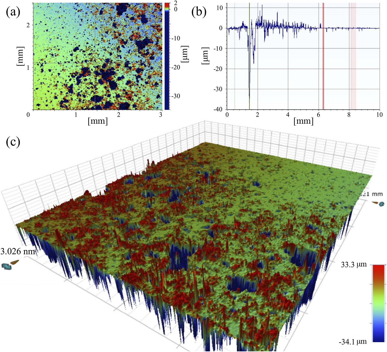
Figure 4 Detailed view on a mm-scale region in the vicinity of rough surface features (‘marks’) on the lens-sided sputter plate, using (a), (c) white-light interferometry and (b) a profilometer.
The transition from regions that show no ablation to regions that are heavily ablated is detailed with colour microscopy images in Appendix C.
Concerning the surfacic deposition, we measured the transmittance through the centre of the rear-side sputter plate (marked with an X point in Figure 3(a)) with spectral resolution using a compact Czerny–Turner spectrometer, as shown in Figure 5. The integrated surface element is $1\;{\mathrm{mm}}^2$
. The measurement shows a flat spectral response in accordance with the theoretical prediction presented in Section 2 for the transition metal nickel deposited on an FS plate.
$1\;{\mathrm{mm}}^2$
. The measurement shows a flat spectral response in accordance with the theoretical prediction presented in Section 2 for the transition metal nickel deposited on an FS plate.
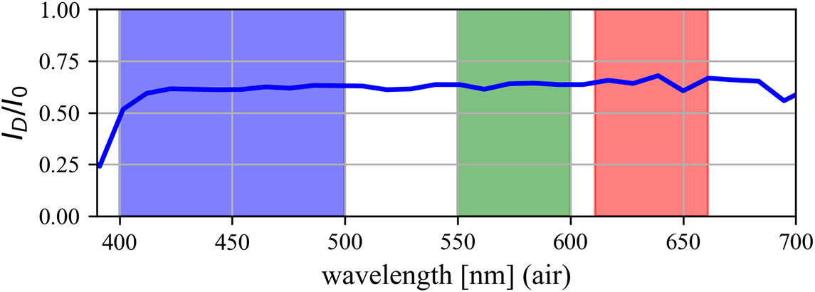
Figure 5 Spectrally resolved transmittance of nickel debris illuminated with the light source in an EPSON V-750-PRO flatbed scanner; indicated are blue, green and red bands of acquisition for the scanner head. A measurement of intensities ${I}_0$
through silica glass is used to normalize the measurement through debris
${I}_0$
through silica glass is used to normalize the measurement through debris ${I}_{\mathrm{D}}$
.
${I}_{\mathrm{D}}$
.
The transmittance of the debris in Figure 3(a) is shown in Figure 6 in a squared region of interest (ROI) selecting a region of uniform deposition (green squares in Figure 3) far from the central marks. For conversion from scan intensity to transmittance we follow Equation (A3) from Appendix A, which reads as follows:
 $$\begin{align}{T}_{{mn}}={10}^{\left(\ln \left[{I}_{{mn}}\right]/B\right)-C}.\end{align}$$
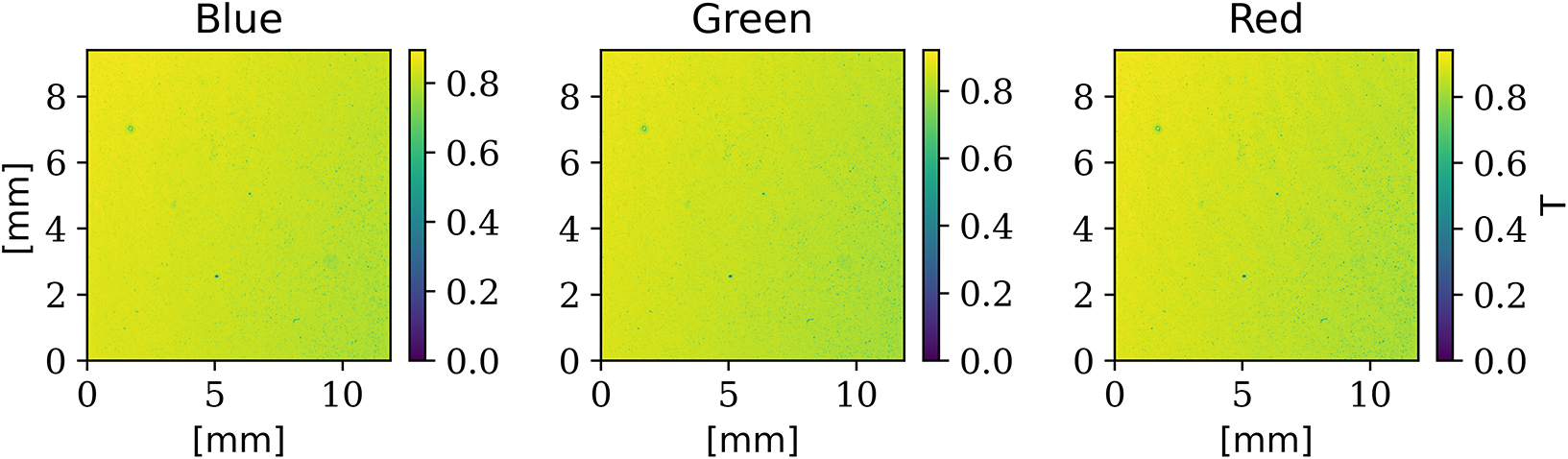
Figure 6 Transmittance through the debris on the rear-side (with respect to the laser interaction) silica plate for all three channels of the RGB scan.
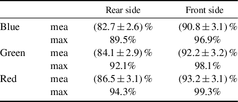
The raw data are analysed separately for the distinct RGB channels, revealing no opaque zones, which allows for quantitative analysis of the full surface. For all three channels the transmittance shows a similar behaviour, as can be seen in Table 1. The surfacic deposition on the rear side has a uniform mean transmittance of $\left(84.4\pm 2.9\right)\%$
in the ROI. Towards the front side, the mean transmittance amounts to
$\left(84.4\pm 2.9\right)\%$
in the ROI. Towards the front side, the mean transmittance amounts to $\left(92.1\pm 1.8\right)\%$
in the ROI.
$\left(92.1\pm 1.8\right)\%$
in the ROI.
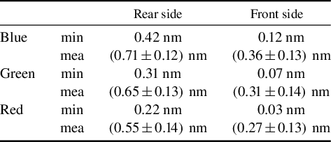
Table 1 Mean (mea) and maximum (max) transmittance values for the front- and rear-side (with respect to the laser interaction) sputter plates across the three colour channels of an RGB scan.
Considering that the debris on the sputter plates consists only of deposited nickel, we calculate the thickness of the deposited debris using Equation (B1) from Appendix B, which reads as follows:
 $$\begin{align}T\left( z_\mathrm{M}, z_\mathrm{S}\right)={\int}_{\omega_{-}}^{\omega_{+}}\parallel \mathfrak{T}\left( z_\mathrm{M}, z_\mathrm{S},\omega \right){\parallel}^2\cdot s\left(\omega \right)\mathrm{d}\omega .\end{align}$$
The results are shown in Figure 7, and the characteristic values are given in Table 2. The surfacic deposition on the rear-side ROI has a uniform mean thickness of $\left(0.6\pm 0.1\right)\;\mathrm{nm}$
. Towards the front side, the mean thickness in the ROI amounts to
$\left(0.6\pm 0.1\right)\;\mathrm{nm}$
. Towards the front side, the mean thickness in the ROI amounts to $\left(0.3\pm 0.1\right)\;\mathrm{nm}$
.
$\left(0.3\pm 0.1\right)\;\mathrm{nm}$
.
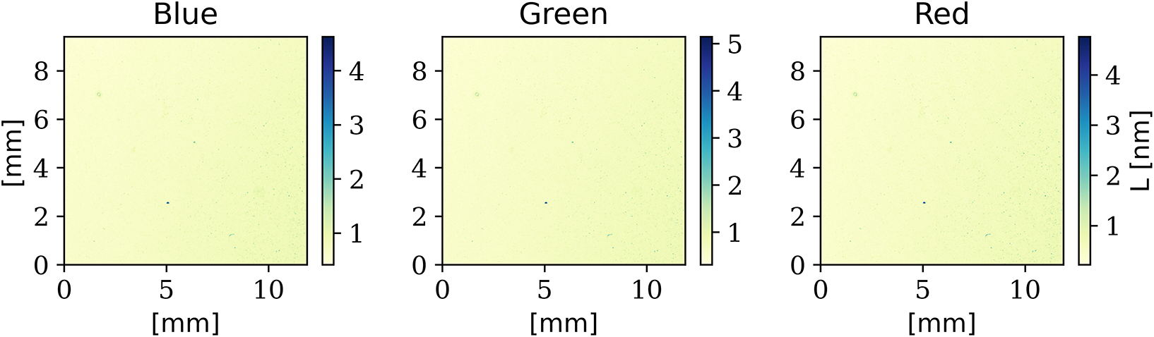
Figure 7 Thickness of the nickel debris on the rear-side silica plate calculated from the transmittance separately for all three channels of the RGB scan.
Table 2 Characteristic minimum (min) and mean (mea) thickness values deduced from the transmittance for the front- and rear-side sputter plates across the three colour channels of an RGB scan.
The mass can be calculated as ${z}_{\mathrm{Ni}}\cdot {p}^2\cdot \rho$
with the pixel size
${z}_{\mathrm{Ni}}\cdot {p}^2\cdot \rho$
with the pixel size $p=10.6\;\mu \mathrm{m}$
and assuming solid density
$p=10.6\;\mu \mathrm{m}$
and assuming solid density $\rho =8.9\;\mathrm{g}\;{\mathrm{cm}}^{-3}$
. The total mass of nickel deposited on both plates, within the ROIs from Figure 6, amounts to
$\rho =8.9\;\mathrm{g}\;{\mathrm{cm}}^{-3}$
. The total mass of nickel deposited on both plates, within the ROIs from Figure 6, amounts to $3.3\;\mu \mathrm{g}$
,
$3.3\;\mu \mathrm{g}$
, $\left(2.6\pm 0.8\right)\;\mu \mathrm{g}$
towards the rear side and
$\left(2.6\pm 0.8\right)\;\mu \mathrm{g}$
towards the rear side and $\left(1.3\pm 0.4\right)\;\mu \mathrm{g}$
towards the front side. In terms of corresponding debris emission, the average production is
$\left(1.3\pm 0.4\right)\;\mu \mathrm{g}$
towards the front side. In terms of corresponding debris emission, the average production is $\left(24\pm 5\right)\;\mu \mathrm{g}\;{\mathrm{sr}}^{-1}$
towards the front side and
$\left(24\pm 5\right)\;\mu \mathrm{g}\;{\mathrm{sr}}^{-1}$
towards the front side and $\left(83\pm 15\right)\;\mu \mathrm{g}\;{\mathrm{sr}}^{-1}$
towards the rear side. Note the non-linear relationship between measured transmittance and derived debris thickness. The emission detected within the surfacic deposition is slightly asymmetric, with larger ejection towards the rear side of the target.
$\left(83\pm 15\right)\;\mu \mathrm{g}\;{\mathrm{sr}}^{-1}$
towards the rear side. Note the non-linear relationship between measured transmittance and derived debris thickness. The emission detected within the surfacic deposition is slightly asymmetric, with larger ejection towards the rear side of the target.
4 Discussion
Available modelling[
Reference Ehret, Apiñaniz, Henares, Lera, de Luis, Pérez-Hernández, Volpe and Gatti
26
] suggests that shots on small disk targets emit more debris than shots on large disk targets. The prediction for small disks is the total emission of $\left(257\pm 50\right)\;\mu \mathrm{g}$
, while it is
$\left(257\pm 50\right)\;\mu \mathrm{g}$
, while it is $\left(99\pm 20\right)\;\mu \mathrm{g}$
for large disks. This difference between large disks and small disks can be explained by a larger fraction of the laser-heated electrons being held back by stronger fields in the case of smaller targets. With a larger refluxing cloud of near-relativistic electrons there are more electrons available to transfer heat to the bulk material. The model applies to cases where the evaporating mass is not limited by the available target mass (here
$\left(99\pm 20\right)\;\mu \mathrm{g}$
for large disks. This difference between large disks and small disks can be explained by a larger fraction of the laser-heated electrons being held back by stronger fields in the case of smaller targets. With a larger refluxing cloud of near-relativistic electrons there are more electrons available to transfer heat to the bulk material. The model applies to cases where the evaporating mass is not limited by the available target mass (here $>429\;\mu \mathrm{m}$
diameter disks), and where the target sizes are smaller than the maximum expansion of the laser-generated target potential during electron discharge (here
$>429\;\mu \mathrm{m}$
diameter disks), and where the target sizes are smaller than the maximum expansion of the laser-generated target potential during electron discharge (here $<12\;\mathrm{mm}$
disks).
$<12\;\mathrm{mm}$
disks).
Experimentally, the total mass of the debris can be extrapolated from the measured mean surfacic deposition in the ROIs (towards the rear and front sides) of $54\;\mu \mathrm{g}\;{\mathrm{sr}}^{-1}$
assuming a spherically uniform emission. The extrapolated result is
$54\;\mu \mathrm{g}\;{\mathrm{sr}}^{-1}$
assuming a spherically uniform emission. The extrapolated result is $\left(672\pm 127\right)\;\mu \mathrm{g}$
and compares well with the modelled total value of
$\left(672\pm 127\right)\;\mu \mathrm{g}$
and compares well with the modelled total value of $\left(613\pm 83\right)\;\mu \mathrm{g}$
(obtained from the sum of the contribution of two small disks and one large disk) within the margins of uncertainty. The observed small asymmetry of the spherical emission (with more deposition towards the target rear side) might be owed to the asymmetry of the charge distribution in the environment of the laser interaction, with more electrons deposited in the laser forward direction. The asymmetry might be also related to the target thickness, which motivates future parametric studies.
$\left(613\pm 83\right)\;\mu \mathrm{g}$
(obtained from the sum of the contribution of two small disks and one large disk) within the margins of uncertainty. The observed small asymmetry of the spherical emission (with more deposition towards the target rear side) might be owed to the asymmetry of the charge distribution in the environment of the laser interaction, with more electrons deposited in the laser forward direction. The asymmetry might be also related to the target thickness, which motivates future parametric studies.
The damaged areas on the sputter plates might be produced by the impact of high-velocity debris particles or dense flares of debris. The constraint area of damage reveals this population to be rather directional towards both target normal directions. There is visibly slightly more damage on the sputter plate facing the target front side than that facing towards the target rear side. The amount of ablated glass on the front side is $245\%$
larger than that on the rear side. This might point to the observation of a larger quantity of directional debris towards the target normal on the side of the laser interaction, similar to an earlier observation of this behaviour by Booth et al.
[
Reference Booth, Astbury, Bryce, Clarke, Gregory, Green, Haddock, Heathcote and Spindloe
27
]. This directional emission of destructive debris is favourable in situations of tight laser focusing. The latter is required to reach ultrahigh intensities, but brings the precious final focusing optic into close vicinity to the debris source. Directional debris can be mitigated by choosing the laser-incidence angle large enough to avoid an intersection of target normal and focusing optics. The population of debris that is emitted spherically uniformly poses a much lower risk as it can be addressed by available mitigation schemes, that is, spinning protection disks[
Reference Chen, Zhao, Xu, Peng, Ma, Gao, Chen, Liu, Xu, Pan, g, Song, Xu, Yan and Ma
36
].
$245\%$
larger than that on the rear side. This might point to the observation of a larger quantity of directional debris towards the target normal on the side of the laser interaction, similar to an earlier observation of this behaviour by Booth et al.
[
Reference Booth, Astbury, Bryce, Clarke, Gregory, Green, Haddock, Heathcote and Spindloe
27
]. This directional emission of destructive debris is favourable in situations of tight laser focusing. The latter is required to reach ultrahigh intensities, but brings the precious final focusing optic into close vicinity to the debris source. Directional debris can be mitigated by choosing the laser-incidence angle large enough to avoid an intersection of target normal and focusing optics. The population of debris that is emitted spherically uniformly poses a much lower risk as it can be addressed by available mitigation schemes, that is, spinning protection disks[
Reference Chen, Zhao, Xu, Peng, Ma, Gao, Chen, Liu, Xu, Pan, g, Song, Xu, Yan and Ma
36
].
The experimental results show two small directional marks next to one large mark, which is counter-intuitive when compared with the modelling that predicts a larger total emission of debris for smaller targets[ Reference Ehret, Apiñaniz, Henares, Lera, de Luis, Pérez-Hernández, Volpe and Gatti 26 ]. If the presumption is correct that both small marks correspond to both shots on small targets, then the directional fraction of debris is smaller for small disk targets than for large ones. However, the larger recirculating electron population for smaller targets may yield evaporation to higher temperature, and heating for longer times. Therefore, the amount of spherically emitted debris can be higher for smaller targets than for larger targets. A larger fraction of spherically emitted debris will constrain the directional population.
The characteristic hourglass shape of the directional debris marks might encode valuable information about the laser–target interaction. Studies on laser-induced forward and backward transfer in the long-pulse regime show the ejection of debris dependent on the laser pulse width, laser pulse energy density and target–catcher distance[ Reference Sano, Yamada, Nakayama and Miyamoto 37 – Reference Hennig, Baldermann, Nussbaum, Rossier, Brockelt, Schuler and Hochstein 39 ]. Further investigation is required to evaluate if debris can be an auxiliary metrology on the laser focal spot profile and temporal laser contrast.
This work took advantage of the benefit of the uniform absorption curve of nickel across the visible spectrum to introduce a fast spatially resolved method of debris characterization. When using spectrometers instead of a flatbed scanner, surface plasmons might be a way to characterize not only the thickness of a layer but also the size of nano-structures when using materials that exhibit a large surface plasmon strength[ Reference Rycenga, Cobley, Zeng, Li, Moran, Zhang, Qin and Xia 40 ].
5 Conclusion
We present a novel method for the characterization of thin layers of debris deposit based on RGB transmission scans that can be performed with commercial flatbed scanners. Initially transparent debris shields from FS are successfully used as debris catchers during experiments with high-power ultra-relativistic laser pulses irradiating solid-density targets. Scans reveal two distinct types of debris: (i) narrow emission cones away from target front- and rear-side normal direction and (ii) spherical emission. While more debris of type (i) is emitted away from the target front, type (ii) shows a slight asymmetry favouring the target rear side. The former agrees with previous works[ Reference Booth, Astbury, Bryce, Clarke, Gregory, Green, Haddock, Heathcote and Spindloe 27 ], while the latter might be due to the overall asymmetric space charge distribution induced by the laser–plasma interaction.
However, the method developed here is applicable only to materials with a smooth transmittance in the optical regime, and cannot be applied to target materials such as semimetals (aluminium) and noble metals (gold), which exhibit plasmons. Nevertheless, with enough sensor sensitivity, this method can be applied to plastic targets. It is further important for the direct applicability of this method that the surface of the sample is flat, such that the amount of transmitted light is not further reduced by diffuse reflection, which is not taken into account.
The quantitative characterization of the amount of debris and the direction of ejection can be used to promote the implementation of novel schemes that mitigate its deleterious effect on optical components and diagnostics.
Appendix A Scanning procedure
Scans with an EPSON V-750-PRO flatbed scanner are performed in both possible orientations (with the debris facing the scanner light source and with the debris facing the scanner readout) and differences are taken into account as uncertainty of the intensity $\Delta I$
. To improve the estimate of uncertainties of the presented method, RGB colour scans are performed and the results of the differing acquisition bands are compared (B: 400–500 nm; G: 550–600 nm; R: 611–661 nm[
Reference Lárraga-Gutiérrez, García-Garduño, Treviño-Palacios and Herrera-González
41
]). The spectrum
$\Delta I$
. To improve the estimate of uncertainties of the presented method, RGB colour scans are performed and the results of the differing acquisition bands are compared (B: 400–500 nm; G: 550–600 nm; R: 611–661 nm[
Reference Lárraga-Gutiérrez, García-Garduño, Treviño-Palacios and Herrera-González
41
]). The spectrum $s\left(\lambda \right)$
of the scanner lamp is compared to the acquisition bands in Figure 8. Here
$s\left(\lambda \right)$
of the scanner lamp is compared to the acquisition bands in Figure 8. Here ${\lambda =2\pi c/\omega}$
is the vacuum wavelength, with the speed of light
${\lambda =2\pi c/\omega}$
is the vacuum wavelength, with the speed of light $c$
and the frequency of the electromagnetic wave
$c$
and the frequency of the electromagnetic wave $\omega$
.
$\omega$
.
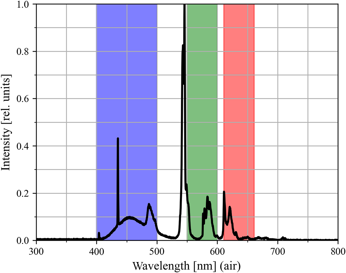
Figure 8 Normalized spectrum of the light source of the EPSON V-750-PRO flatbed scanner used for this work, with an indication of the blue, green and red bands of acquisition for the scanner head.
The transmittance $T$
can be derived from the optical density (OD) of a sample. The OD detected in a pixel of coordinates
$T$
can be derived from the optical density (OD) of a sample. The OD detected in a pixel of coordinates $\left(m,n\right)$
is defined as the logarithmic ratio between the transmitted greyscale intensity
$\left(m,n\right)$
is defined as the logarithmic ratio between the transmitted greyscale intensity $I\left(m,n\right)$
and the scanner response for a scan without sample
$I\left(m,n\right)$
and the scanner response for a scan without sample ${I}_0$
, which can be written as follows:
${I}_0$
, which can be written as follows:
 $$\begin{align}\mathrm{OD}=-{\log}_{10}\left[\frac{I\left(m,n\right)}{I_0}\right]=-{\log}_{10}\left[{T}_{{mn}}\right].\end{align}$$
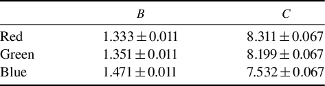
Kodak WRATTEN 2 neutral density No. 96 filters with well-defined spectral properties are used for absolute scanner calibration of transmission scans. The relation of OD to the transmitted greyscale intensity results in the following:
 $$\begin{align}\mathrm{OD}=C-\frac{\ln \left[{I}_{{mn}}\right]}{B},\end{align}$$
where $B$
and
$B$
and $C$
are band-dependent fit parameters, as shown in Table 3. Here,
$C$
are band-dependent fit parameters, as shown in Table 3. Here, $B$
represents the inverse scale parameter for the exponential decay and
$B$
represents the inverse scale parameter for the exponential decay and $C$
is the minimum detectable transmittance. The dynamic range on the greyscale can be computed as
$C$
is the minimum detectable transmittance. The dynamic range on the greyscale can be computed as $\exp \left(B\cdot C\right)$
. One retrieves the transmittance as follows:
$\exp \left(B\cdot C\right)$
. One retrieves the transmittance as follows:
 $$\begin{align}{T}_{{mn}}={10}^{\left(\ln \left[{I}_{{mn}}\right]/B\right)-C},\end{align}$$
with a relative uncertainty as follows:
 $$\begin{align}\frac{\Delta {T}_{{mn}}}{T_{{mn}}}=\ln \left[10\right]\cdot \sqrt{{\left(\frac{\Delta {I}_{{mn}}}{I_{{mn}}B}\right)}^2+{\left(\frac{\ln \left[{I}_{{mn}}\right]\Delta B}{B^2}\right)}^2+{\left(\Delta C\right)}^2}.\end{align}$$
The relative uncertainty is calculated to be $\Delta {T}_{{mn}}/{T}_{{mn}}\approx 16\%$
for all colour channels on the scale of 16-bit images used for this work, considering a scan-to-scan uncertainty of
$\Delta {T}_{{mn}}/{T}_{{mn}}\approx 16\%$
for all colour channels on the scale of 16-bit images used for this work, considering a scan-to-scan uncertainty of $\Delta {I}_{{mn}}/{I}_{{mn}}\approx 1.1\%$
.
$\Delta {I}_{{mn}}/{I}_{{mn}}\approx 1.1\%$
.
Table 3 Greyscale to OD calibration fit parameters for every colour channel of an EPSON V-750-PRO.
Appendix B Transmission of a flat double-layer system of debris and catcher
For nm-scale layers of metal deposits on transparent support plates it is possible to retrieve the debris thickness from a measurement of the transmittance:
 $$\begin{align}T\left( z_\mathrm{M}, z_\mathrm{S}\right)={\int}_{\omega_{-}}^{\omega_{+}}\parallel \mathfrak{T}\left( z_\mathrm{M}, z_\mathrm{S},\omega \right){\parallel}^2\cdot s\left(\omega \right)\mathrm{d}\omega ,\end{align}$$
where ${z}_{\mathrm{M}}$
is the thickness of the metal deposit,
${z}_{\mathrm{M}}$
is the thickness of the metal deposit, ${z}_{\mathrm{S}}$
is the thickness of the support plate and
${z}_{\mathrm{S}}$
is the thickness of the support plate and $\omega$
denotes the frequency of the incident electromagnetic waves in a normalized spectrum
$\omega$
denotes the frequency of the incident electromagnetic waves in a normalized spectrum ${\int}_{\omega_{-}}^{\omega_{+}}s\left(\omega \right)\mathrm{d}\omega =1$
. In the following equations, the subscript M relates to the metal, and the subscript S relates to the support plate, for all quantities. The transmission ratio
${\int}_{\omega_{-}}^{\omega_{+}}s\left(\omega \right)\mathrm{d}\omega =1$
. In the following equations, the subscript M relates to the metal, and the subscript S relates to the support plate, for all quantities. The transmission ratio $\mathfrak{T}$
for a mono-chromatic incident wave is defined as follows:
$\mathfrak{T}$
for a mono-chromatic incident wave is defined as follows:
 $$\begin{align}\mathfrak{T}\left( z_\mathrm{M}, z_\mathrm{S},\omega \right)={E}_{\mathrm{t}}/{E}_0^{+},\end{align}$$
with the electric field amplitude of the incident wave ${E}_0^{+}$
and the amplitude at the exit of the double-layer system
${E}_0^{+}$
and the amplitude at the exit of the double-layer system ${E}_{\mathrm{t}}$
. For normally incident electromagnetic fields, the continuity of the electric and magnetic fields across interfaces between layers of media
${E}_{\mathrm{t}}$
. For normally incident electromagnetic fields, the continuity of the electric and magnetic fields across interfaces between layers of media $j$
and
$j$
and $j+1$
implies the following at the boundary:
$j+1$
implies the following at the boundary:
 $$\begin{align}{\mathfrak{E}}_j^{+}+{\mathfrak{E}}_j^{-}&={\mathfrak{E}}_{j+1}^{+}+{\mathfrak{E}}_{j+1}^{-},\nonumber\\ {}\frac{1}{\eta_j}\left({\mathfrak{E}}_j^{+}-{\mathfrak{E}}_j^{-}\right)&=\frac{1}{\eta_{j+1}}\left({\mathfrak{E}}_{j+1}^{+}-{\mathfrak{E}}_{j+1}^{-}\right),\end{align}$$
with electric resistance ${\eta}_j=\sqrt{\mu_j/{\epsilon}_j}$
, where
${\eta}_j=\sqrt{\mu_j/{\epsilon}_j}$
, where ${\mu}_j$
is the permeability and
${\mu}_j$
is the permeability and ${\varepsilon}_j$
the permittivity of the respective material. Here the electric field component is described in terms of plane waves
${\varepsilon}_j$
the permittivity of the respective material. Here the electric field component is described in terms of plane waves ${\mathfrak{E}}_j^{\pm}={E}_j^{\pm }{e}^{\mp i\left({z}^{\prime }{k}_j-\omega t\right)}$
with wavenumber
${\mathfrak{E}}_j^{\pm}={E}_j^{\pm }{e}^{\mp i\left({z}^{\prime }{k}_j-\omega t\right)}$
with wavenumber ${k}_j$
. Components
${k}_j$
. Components ${\mathfrak{E}}_j^{+}$
are forward propagating (in direction from
${\mathfrak{E}}_j^{+}$
are forward propagating (in direction from $j$
to
$j$
to $j+1$
) while components
$j+1$
) while components ${\mathfrak{E}}_j^{-}$
propagate backwards. One obtains the following:
${\mathfrak{E}}_j^{-}$
propagate backwards. One obtains the following:
 $$\begin{align}{c}{E}_0^{+}+{E}_0^{-}&={E}_{\mathrm{M}}^{+}+{E}_{\mathrm{M}}^{-},\nonumber\\ {}\frac{1}{\eta_0}\left({E}_0^{+}-{E}_0^{-}\right)&=\frac{1}{\eta_{\mathrm{M}}}\left({E}_{\mathrm{M}}^{+}-{E}_{\mathrm{M}}^{-}\right),\kern1em \end{align}$$
 $$\begin{align}\sum \limits_{p\in \left\{+1,-1\right\}}{E}_{\mathrm{M}}^p{e}^{-{ipz}_{\mathrm{M}}{k}_{\mathrm{M}}}&={E}_{\mathrm{S}}^{+}+{E}_{\mathrm{S}}^{-},\nonumber\\ {}\sum \limits_{p\in \left\{+1,-1\right\}}\frac{p}{\eta_{\mathrm{M}}}{E}_{\mathrm{M}}^p{e}^{-{ipz}_{\mathrm{M}}{k}_{\mathrm{M}}}&=\frac{1}{\eta_{\mathrm{S}}}\left({E}_{\mathrm{S}}^{+}-{E}_{\mathrm{S}}^{-}\right),\end{align}$$
 $$\begin{align}\sum \limits_{p\in \left\{+1,-1\right\}}{E}_{\mathrm{S}}^p{e}^{-{ipz}_{\mathrm{S}}{k}_{\mathrm{S}}}&={E}_{\mathrm{t}},\nonumber\\ {}\sum \limits_{p\in \left\{+1,-1\right\}}\frac{p}{\eta_{\mathrm{S}}}{E}_{\mathrm{S}}^p{e}^{-{ipz}_{\mathrm{S}}{k}_{\mathrm{M}}}&=\frac{1}{\eta_0}{E}_{\mathrm{t}},\end{align}$$
at the entrance (Equation (B4)), middle interface (Equation (B5)) and exit (Equation (B6)) of the double-layer system, where ${E}_0^{-}$
denotes the reflected wave.
${E}_0^{-}$
denotes the reflected wave.
For a first layer of the ferromagnetic transition metal nickel (Ni) followed by a second layer of FS one derives the following:
 $$\begin{align}&\mathfrak{T}\left({z}_{\mathrm{Ni}},{z}_{\mathrm{FS}},\omega \right)=8{e}^{-{iz}_{\mathrm{FS}}{k}_{\mathrm{FS}}}\nonumber\\&\quad\cdot \Big(m_{+}{e}^{iz_{\mathrm{Ni}}{k}_{\mathrm{Ni}}}\left({n}_{+}{u}_{+}+{n}_{-}{u}_{-}{e}^{-2{iz}_{\mathrm{FS}}{k}_{\mathrm{FS}}}\right)\nonumber\\&\quad+{m}_{-}{e}^{-{iz}_{\mathrm{Ni}}{k}_{\mathrm{Ni}}}\left({n}_{-}{u}_{+}+{n}_{+}{u}_{-}{e}^{-2{iz}_{\mathrm{FS}}{k}_{\mathrm{FS}}}\right)\Big)^{-1},\end{align}$$
 $$\begin{align}\parallel \mathrm{with}\kern1em {m}_{\pm}=1\pm {n}_{\mathrm{Ni}},\end{align}$$
 $$\begin{align}{n}_{\pm}=1\pm \frac{n_{\mathrm{FS}}}{n_{\mathrm{Ni}}},\end{align}$$
 $$\begin{align}{u}_{\pm}=1\pm \frac{1}{n_{\mathrm{FS}}},\end{align}$$
 $$\begin{align}{k}_j=\frac{n_j\omega }{c}-i\frac{\alpha_j}{2},\end{align}$$
where ${\alpha}_j$
is the absorption coefficient of layer
${\alpha}_j$
is the absorption coefficient of layer $j$
and
$j$
and ${n}_j$
denotes the refractive index. The following approximations of both spectrally resolved quantities are evaluated for wavelengths in the range from 400 to 661 nm (from
${n}_j$
denotes the refractive index. The following approximations of both spectrally resolved quantities are evaluated for wavelengths in the range from 400 to 661 nm (from $\omega =4.71\times {10}^{15}$
to
$\omega =4.71\times {10}^{15}$
to $2.85\times {10}^{15}\;{\mathrm{s}}^{-1}$
).
$2.85\times {10}^{15}\;{\mathrm{s}}^{-1}$
).
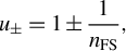
The absorption of films of evaporated nickel is as follows[ Reference Johnson and Christy 42 ]:
 $$\begin{align}{\alpha}_{\mathrm{Ni}}\approx \left(\frac{\omega }{\left(1.64\pm 0.05\right)\times {10}^{18}\;{\mathrm{s}}^{-1}}+0.08017\right){\mathrm{nm}}^{-1}.\end{align}$$
Such a monotonic behaviour is common for transition metals that do not build surface plasmons efficiently[
Reference Axelevitch, Gorenstein and Golan
43
]. Note that the absorption coefficient ${\alpha}_{\mathrm{FS}}$
of silica glass is neglected in the following because of its small magnitude[
Reference Kitamura, Pilon and Jonasz
44
]. The refractive indices of nickel[
Reference Johnson and Christy
42
] and FS[
Reference Malitson
45
] are as follows:
${\alpha}_{\mathrm{FS}}$
of silica glass is neglected in the following because of its small magnitude[
Reference Kitamura, Pilon and Jonasz
44
]. The refractive indices of nickel[
Reference Johnson and Christy
42
] and FS[
Reference Malitson
45
] are as follows:
 $$\begin{align}{n}_{\mathrm{Ni}}\approx \frac{\left(2.43\pm 0.08\right)\times {10}^{15}\;{\mathrm{s}}^{-1}}{\omega }+1.183,\end{align}$$
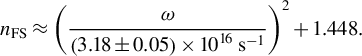 $$\begin{align}{n}_{\mathrm{FS}}\approx {\left(\frac{\omega }{\left(3.18\pm 0.05\right)\times {10}^{16}\;{\mathrm{s}}^{-1}}\right)}^2+1.448.\end{align}$$
The evaluation of Equation (B1) can now be performed numerically in spectral slices, that is, for every colour channel of a scan (compare Figure 8 for the spectrum and the acquisition bands of an EPSON V-750-PRO flatbed scanner). Note that some application cases might be well fitted with an approximated analytical solution for a thin film on a thick finite transparent substrate[ Reference Swanepoel 46 ].
Appendix C Instrumentation for standard surface analysis
1 Elemental analysis
Elemental analysis was performed with a Pemtron PS-230AL SEM, fitted with a Bruker QX2 EDX system. It comprises a five-axis motorized stage and tungsten cathode, and a PC-controlled compact variable pressure vacuum system.
Method: No gold sample coating was required, as charging was present but not sufficient to affect the energy-dispersive X-ray (EDX) spectra. The setup consisted of an electron beam of 20 keV without aperture, a low magnification and a short acquisition time of 60 s to avoid over charging. The count rate of X-ray photons detected by the EDS detector for the measurement was 3000 counts per second.
Results: The atomic percentages of the following materials were found:
-
• nickel $36.14\%$
;
$36.14\%$
; -
• silicon
$26.41\%$
; -
• oxygen
$32.97\%$
; -
• chlorine
$2.22\%$
; -
• aluminium
$2.26\%$
.


Note that silicon, oxygen and aluminium are likely present due to the glass substrate and SEM chamber background. Both samples (lens and polarizer sputter plates) are considered to have similar results, but this was not explored in detail.
2 Three-dimensional area scan
A three-dimensional (3D) area scan was performed using a 3D optical profilometer, the Bruker ContourX-100.
Method: The setup consisted of 5× objective, 0.55× field of view, 100 μm back scan and forward scan and a threshold value of $2\%$
(this threshold means that any height variation that is more than
$2\%$
(this threshold means that any height variation that is more than $2\%$
of the standard deviation away from the average will be considered significant). This is considered a lenient threshold that would include a lot of noise, but given the sharpness of the features in the sample and the steep wall angles, a higher threshold value excluded too much of the features. Stitching areas were approximately
$2\%$
of the standard deviation away from the average will be considered significant). This is considered a lenient threshold that would include a lot of noise, but given the sharpness of the features in the sample and the steep wall angles, a higher threshold value excluded too much of the features. Stitching areas were approximately $15\kern0.24em \mathrm{mm}\times 12$
mm in size consisting of 20+ individual measurements, with a
$15\kern0.24em \mathrm{mm}\times 12$
mm in size consisting of 20+ individual measurements, with a $20\%$
overlap between scans. The area was chosen to include all areas of ablation visible. Data fill was used to approximate missing data in areas of high damage using the software provided data fill algorithm in Vision64 Software.
$20\%$
overlap between scans. The area was chosen to include all areas of ablation visible. Data fill was used to approximate missing data in areas of high damage using the software provided data fill algorithm in Vision64 Software.
Results: Data fill was considerable and introduces a lot of uncertainty. The samples are inherently rough and difficult to measure with optical techniques, so no filtering was applied. The depth of ablation areas had poor data acquisition, and consequently the step profilometer was considered for more accurate measurements.
3 Surface profile
The surface profile was performed with a Dektak Pro Stylus Profilometer.
Method: The setup consisted of a stylus of 2 μm diameter and 10 mm length, stylus force of 10 mg, resolution longitudinal of 0.555 μm/pt and resolution quoted as sub 100 nm in height. Data were averaged over five scans.
Results: Stylus radius of 2 μm may smooth out the sharpest features. Debris and ablation seem to be immovable and adhered to the substrate such that the probe would not change the substrate during measurement. Multiple measurements were taken and an average of ablation depth was estimated at 10 μm.
4 Microscope image
Optical microscopy is deployed to capture views on the sputter plate; colour images of the front-side sputter plate are shown in Figure 9. One notes an abrupt transition from damage-free regions to regions with low damage density. Then there is a gradual increase of the damage density towards a region that is heavily damaged.
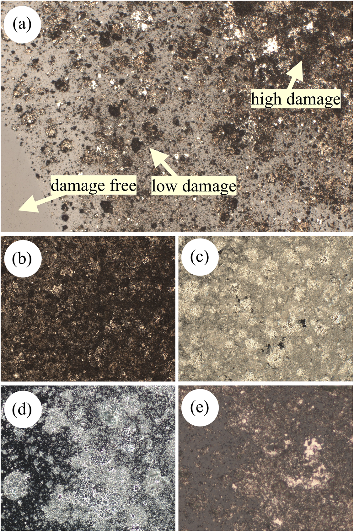
Figure 9 Detailed microscope images of the polarizer-sided sputter plate. (a) A region that shows the transition from damage-free to high-damage areas captured with a 5× magnified bright field acquisition (full width corresponds to 3 mm). A high-damage area as (b) 5× magnified bright field and (c) 5× magnified dark field (full width corresponds to 3 mm), as well as a low-damage area as (d) 20× magnified dark field (full width corresponds to 0.75 mm) and (e) 50× magnified bright field (full width corresponds to 0.3 mm).
Author contributions
M.E. commissioned the methodology; C.V. and A.H. acquired the data; I.M.V. performed the data curation and analysis; I.M.V. wrote the first draft of the manuscript; J.L.D., I.M.V. and M.E. revised the methodology; P.W.B. and M.E. organized the beamtime at ELI-NP; S.A., H.A., J.I.A., M.C., J.L.D., M.G., M.K., R.L., A.M., D.S. and D.U. were involved with underlying experimental work; D.H. and S.A. independently performed standard surface analysis; all authors contributed to manuscript improvement and read and approved the submitted version.
Acknowledgements
This work would not have been possible without the help of the laser and the engineering teams at Centro de Láseres Pulsados (CLPU) and ELI-NP, and the target fabrication team at CLF (Central Laser Facility, UK). Special thanks for much appreciated support to the workshops of CLPU and ELI-NP. The authors are grateful to D. de Luis and to P. Puyuelo Valdés for help in preparing the experimental campaign. This work received funding from the European Union’s Horizon 2020 research and innovation programme through the European IMPULSE project under grant agreement No. 871161 and LASERLAB-EUROPE V under grant agreement No. 871124; from grant PDC2021-120933-I00 funded by MCIN / AEI / 10.13039/501100011033 and by the European Union Next Generation EU/PRTR; from grant PID2021-125389OA-I00 funded by MCIN / AEI / 10.13039/501100011033 / FEDER, UE and by ‘ERDF A way of making Europe’ by the European Union and in addition to Unidad de Investigación Consolidada de la Junta de Castilla y León No. CLP087U16. The UPM47 campaign was funded through IOSIN, Nucleu PN-IFIN-HH 23-26 Code PN 23 21, and the ELI-NP Phase II, a project co-financed by the Romanian Government and the European Union through the European Regional Development Fund and the Competitiveness Operational Programme (1/07.07.2016, COP, ID 1334). This research was funded, in part, by the French Agence Nationale de la Recherche (ANR), Project No. ANR-22-CE30-0044. This research work was also supported by the Ministry of Youth and Sports of the Czech Republic (Project Nos. LM2023068 and LM2018114 (PALS RI)).
Data availability statement
The raw data and numerical methods that support the findings of this study are available from the corresponding author upon reasonable request.


 Open access