


Introduction
Mobile and other wireless communication signal radiations and receptions are possible only with antennas. Advanced 5G mobiles require compact and versatile antennas that can radiate multiple frequency bands, and this can be done with the help of planar antennas. UWB systems transmit data at high rates, consume very less power, and general data security is also good, thus they are being employed in widespread areas such as radar imaging, medical imaging, indoor positioning among many. This widespread usage has demanded the development of suitable antennas to be used in the UWB systems. Various designs have been presented for the wideband, curved slot, triangular-shaped, circular, “U”, and “L” shaped, and printed semi-circular slots [Reference Azim, Islam and Misran1–Reference Baudha, Yadav and Srivastava6]. High frequency is achieved by printing a tiny fractal element in an antenna [Reference Shagar and Wahidabanu7]. The antenna is called a defective ground structure by making slots in the ground plane, which resonates with lower oscillations as reported in [Reference Chakraborty, Rana, Sarkar and Das8]. By making a circular trim in the designed radiator, high gain is achieved up to 4.5 dB [Reference Kurniawan and Mukhlishin9]. Two resonance bands are achieved by cutting slots in the antenna, rectangular patch, and attaching circles in the backplane [Reference Ghosh, Ghosh, Ghosh and Chattopadhyay10, Reference Baudha and Yadav11]. Wide-band is reported by making corrugated structure and a half-curved element slot in the radiator [Reference Abdelraheem and Abdalla12].
Small-fractal elements are added to the structure, and multiple slots are also introduced to enhance the bandwidth [Reference Fallahi and Atlasbaf13, Reference Awad and Abdelazeez14]. Truncated ground with a modified patch for improved performance was reported [Reference Baudha, Basak, Manocha and Yadav15]. Stable radiations have been achieved by extending the circular element with backplane and cutting a rectangular element [Reference Yadav and Baudha16, Reference Deshmukh, Singh, Zaveri, Gala and Ray17]. UWB spectrum applications have been reported as a result of trimming semi-circular shape slots in the ground plane and making a modified patch element with the defected backplane [Reference Hota, Yadav, Baudha and Mangaraj18, Reference Baudha and Yadav19]. Planar radiator with a unique shape like a “dumbbell-shaped” planar antenna makes a flexible radiator [Reference Baudha, Garg and Yadav20, Reference Lakshmanan and Sukumaran21]. The signal path is increased by making a long strip and cut slots in a backplane for a stable pattern are reported [Reference Hota, Baudha, Mangaraj and Varun Yadav22].
Balanced radiation pattern has been achieved by a modified patch with partial ground plane (PGP) backplane and properly cutting circular slots on the backplane in planar antenna [Reference Hota, Baudha, Mangaraj and Yadav23, Reference Sudeep, Goswami and Yadav24]. As reported, higher frequencies were achieved by adding rectangular plates at the edges [Reference Mazinani and Hassani25]. High gain is achieved by designing slotted circular fractal antenna [Reference Samyuktha, Kumar Das, Mishra and Kumar Behera26]. Large impedance is reported by cutting multiple slots from front-side antenna [Reference Cheng, Hallbjorner and Rydberg27]. As reported, the lower band starts resonating by making an L-shape strip [Reference Kim and Yun28]. 5G is simulated and fabricated, which achieved an impedance bandwidth of 42% [Reference Golait, Gaikwad, Patil, Varun Yadav, Baudha and Kumar Bramhane29]. 5G antenna is presented for N78 and N79 bands, which cover frequency from 3.4 to 4.9 GHz band. In “Design principle and structure” section, the antenna dimensions are specified, as well as a six-stage development method and simulation results. The simulations of various antenna metrics, as well as related discussion, are covered in “Development of antenna” section. Testing and measured results are discussed in “Simulated parameter study” section. The paper comes to a close after a thorough examination of several simulated and measured results for the design.
Design principle and structure
The proposed radiator's configuration with labeled parameters is shown in Fig. 1. The FR4 substrate is used in the proposed unique antenna design, which has μr = 1, loss tangent = 0.025, and ɛr = 4.3. Figure 1 depicts the geometry of numerous elements; the overall dimension is 25 × 25 × 1.6 mm3. The upper side of FR4 (annealed) is copper having a conductivity of 5.8 × 10⁷ S/m. The impedance bandwidth of the radiator is 128%, with a central frequency of 7.54 GHz (2.91–12.17 GHz). The “L” represented length and width by “W”. The thickness of the substrate is denoted by “H”. The presented radiator's patch is rotated frame type. To develop a modified frame structure, firstly, the patch antenna is converted to a square frame by trimming out a piece of square shape from inside. The side of the outer square frame is denoted by “a1”. The square frame is then rotated by 15° (degrees). Further stage of the structure is done by making a fractal geometry out of the frames. Furthermore, inside the outer frame, a square frame of side length “a2” is made and rotated such that it comes just in contact with the outer frame. The same process is completed three more times with side lengths of subsequent frames to be “a3”, “a4”, and “a5” to complete the fractal frame structure. Five fractal levels were selected as going any deeper with smaller frames inside was not improving the results anymore.

Fig. 1. Front, side and backplane of the proposed antenna with labeled parameters.
The substrate thickness is 1.6 mm. The patch is fed through a 50 Ω strip line with a width of “ws” in mm. The thickness of the ground plane and of the patch is 0.0018 mm. All the square frames are of width 1 mm. Then there has been an addition of two parasitic elements of rectangular shapes, which helped to resonate at lower frequencies. There is a rectangular patch with length “k” and width “W” in the backplane. Two rectangular slots of length “d” and width “g” are cut into it. These rectangular slots are properly adjusted on both sides of the microstrip line of the front plane. A rhombical-shaped slot is also cut into this patch and placed between these rectangular slots. There is another fractal frame design in the backplane placed in the upper left region of the backplane. “m and n” represent the length and width of this structure. The line width of the fractal structure is represented by “z”, and spacing between these lines is denoted by “i” and “j” for the vertical and horizontal spacing, respectively. This fractal structure is connected to the main patch in the ground plane using three strips, each of width “t”. The spacing between these strips is “s”, and their length is “v”. All the other dimensions with their optimum dimensions are shown in Table 1.
Table 1. Design parameters of the presented antenna (all values are in mm)

Development of antenna
Figure 2 shows the 06-stages development of the designed antenna. The development was done using simulation on Computer Simulation Technology (CST) software. Figures 3 and 4 show the antenna's reflection coefficient (S 11) for all the developmental stages.

Fig. 2. 06-stages development of 5 G antenna.

Fig. 3. (S 11) of stage 01, stage 02, and stage 03.

Fig. 4. (S 11) of stage 04, stage 05, and stage 06.
Stage-01 shows a regular rectangular patch antenna with a partial ground plane. A square patch of side length 11 mm is fed through a 3 mm wide strip line and 8.75 mm of length. The partial ground plane length is 8 mm, and starts oscillations from 3.9 to 13.8 GHz. Stage-02 is made by turning the square patch into a square frame of width 1 mm by cutting out a square cross-section from the middle of the square patch. This frame is then rotated by 15 degrees. A further modification is done by repeating the above process for smaller square patches inside the outer one and turning them by enough to touch the outer frame. Due to this, the lower and higher frequencies get shifted, and start oscillations from 3.8 to 14.4 GHz. Stage-03 shows modifications done in the backside. A slot was cut out in the partial ground patch, of width 3 mm and length 1.1 mm, at the top middle part. Further, there is an addition of a fractal shape of 7.2 mm and a width of 10.8 mm. This fractal structure is made of rectangular frames of width 0.225 mm, due to this lower band shifted to below 3.5 GHz.
The addition strips in the backplane to shifted lower band to below 3 GHz as visible in stage-04. These strips connected the fractal shape structure to the main patch in the backplane with a length of 9.3 mm and a thickness of 1 mm. They are placed 1.5 mm apart from each other. Stage-05 helps improve results at higher frequencies by introducing parasitic elements in the front plane. An 11 mm wide rectangular patch with 3.1 mm of length is added directly below and aligned with the patch. Another parasitic element was added, which is triangular. The length of its sides is 3.1, 11, and 11.4 mm, respectively.
This was also aligned with the previous rectangular element and the patch. Stage 06 is completed by making slots in the backplane. Two rectangular slots are cut into the plane of size 6.5 mm × 9.5 mm. There was a more cut out in the shape of a rhombical space with a side length of 1.98 mm. The corners that were along the antenna's length were joined by a strip of width 0.2 mm. Because the slots are in the backside, higher bound increased to more than 12 GHz, which shows the final 5G rotated frame radiator.
Simulated parameter study
We performed a parameter study to optimize the parameters that could impact the results during the designing of the radiator. Here in this section, we discussed the variation of 04-parameters and optimized the design based on their impact on the reflection coefficient (magnitude of S 11) results.
Figure 5 shows the variation in the reflection coefficient (S 11) of the designed antenna by variation in “a1” parameter, which varied from 9 to 13 mm. “a1” is the side length of the front square frame fractal. When it is reduced, the antenna is not in operating performance from 4 to 8 GHz. Due to the variation of parameter “a1”, there is variation in the impedance matching, and the reflection coefficient curves show a large number of return losses. Based on this observation, we conclude that the optimized result (reflection coefficient) is obtained when the side length is fixed at 11 mm.

Fig. 5. Variation in “a1” in terms of (S 11).
Figure 6 shows the variation of reflection coefficient curves with variation in “Ls”, which varied from 7 to 10.5 mm. “Ls” is the length of the feeding line. Change in the length of feeding line causes, in this design, change in size and location of parasitic elements, resulting in a change in results, as impedance matching between the partial backplane and microstrip line is affected. When it is longer at 10.5 mm, the results are helpful only from 3 to 4 GHz. If the size is reduced by much to 7 mm, the result is better but not in range. Thus, 8.75 mm is chosen as an optimized value.

Fig. 6. Variation in “Ls” in terms of (S 11).
Figure 7 shows the variation of reflection coefficient curves with “k” parameter. “k” represents the backplane's length. “k” ranges from 6 to 10 mm. By changing the length in the backplane also changes the dimensions of the slots cut into it. The size of “k” is kept at 6 mm; the radiator is helpful for a small bandwidth from 7 to 8 GHz. As the size of “k” is increased, a bandwidth of 2.9–12.2 GHz at 8 mm was observed. As the size of “k” further increases, results deteriorate. Thus the optimized results are obtained at 8 mm.

Fig. 7. Variation in “k” in terms of (S 11).
Figure 8 shows the variation in parameter “s”, which results in variation in S-parameter results. “s” represents the distance between the three strips connecting the main patch with the fractal structure in the backplane changing from 1 to 2 mm. Generally, in this case, impedance mismatching is visible at higher frequencies. Thus the optimized results are seen at 1.5 mm.

Fig. 8. Variation in “s” in terms of (S 11).
Results
The presented 5G rotated frame radiator is simulated with an FR4 substrate using CST Simulator. A proposed radiator worked in the range of 4.2–12 GHz. Altering the design in the patch to a tilted square frame fractal helped to reduce the lower bound of the operating frequency range to 3.9 GHz. This, followed by introducing fractal structure in the ground plane, helped reduce the lower bound even further to 3.5 GHz. By connecting the fractal structure to the ground patch lowered the lower bound to 2.9 GHz. By adding some parasitic elements in the front plane increased the frequency up to 9 GHz, and multiple slots are made in the backside which resonate the frequency until 12.2 GHz.
Figure 9 shows the testing setup of 5G rotated frame radiator in the anechoic chamber. The antenna testing was done with VNA, and 50 Ω A-type connector connected to feedline.

Fig. 9. 5G antenna testing in the anechoic chamber.
Figure 10 shows the tested return loss (S 11) for an antenna (stage-06). The curves show the good agreement between tested and simulated results. The impedance is fully matched to the entire bandwidth by making the partial backplane. The final proposed geometry below −10 dB is in the frequency range of 2.91–12.17 GHz, which is almost equal to 9.26 GHz.

Fig. 10. Comparison of simulated and measured (S 11 curve).
Figure 11 shows the input impedance curve of the design. The real impedance is normalized to 50 Ω in the entire range, and the imaginary impedance varies from −25 to 25 Ω. For positive parts antenna shows inductive behavior, and for negative parts it shows capacitive behavior.

Fig. 11. Input impedance curve of (stage 06).
Figure 12 shows simulated and measured plot between gain (in dB) and efficiency of the 5G rotated frame radiator. We can observe a peak gain of 3.8 dBi. Now moving forward, we will discuss the other performance metrics. The proposed 5G antenna achieved a peak radiation efficiency of 85%; as seen from the curve, the radiator's efficiency gradually decreases when the frequency increases as the ohmic loss increases at higher frequencies. Both the plots are in good agreement with simulated ones.

Fig. 12. Gain and efficiency of the 5G antenna.
Figures 13 and 14 show the structure's radiation pattern at 3.48, 6.63, 8.67, and 10.1 GHz frequencies. The pattern is defined in two coordinates 90° to each other, H-plane is defined by XoZ plane (Φ = 0°), and E-plane by YoZ plane (Φ = 90°). At all frequencies, the design is very efficient, and it shows stable omnidirectional and bi-directional radiation patterns.
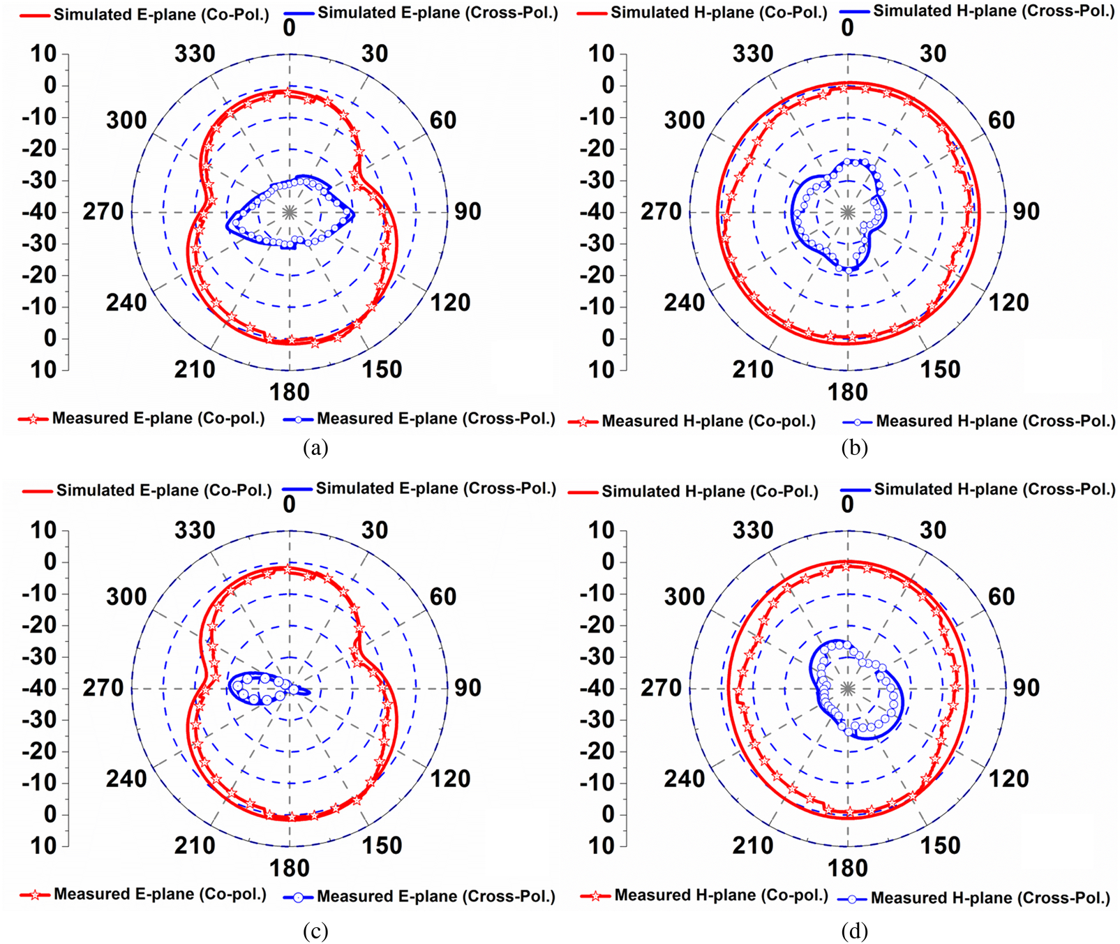
Fig. 13. Co-pol. and Cross-pol. of the 5G antenna at (GHz frequencies), (a) 3.48, E; (b) 3.48, H; (c) 6.63, E; (d) 6.63, H-plane.

Fig. 14. Co-pol. and Cross-pol. of the proposed antenna at (GHz frequencies), (a) 8.67, E; (b) 8.67, H; (c) 10.1, E; (d) 10.1, H-plane.
Table 2 shows a comparison between the proposed design and previously published planar antennas in different parameters by comparing all the parameters with our proposed design. According to the table, our presented 5G rotated frame radiator is capable for UWB-band operation. The 5G rotated frame radiator work aims to design a compact size planar radiator, which is easier to fabricate and capable of transmitting a UWB signal from 2.91 to 12.17 GHz.
Table 2. Comparison between the proposed design and earlier published planar antennas

Figures 15 and 16 show the front and back views of the antenna current distribution at 3.48, 6.63, 8.67, and 10.1 GHz frequencies for E-field and H-field current distribution. Antenna is replaced by equivalent surface, and its radiated current field shows its signal field strengths. The current field distribution is visible throughout the entire antenna, which shows the good signal strength of the design. The proposed rotated frame structure is designed to create a good surface current at three different frequencies. Antenna's radiation pattern is to be stablished and controlled over the entire UWB, by generating a good surface current over the entire antenna. The proposed antenna is able to generate both E-field and H-field strength.

Fig. 15. 3D-vector surface current (front plane).

Fig. 16. 3D-vector surface current (back plane), at (a) 3.48 GHz, (b) 6.63 GHz, (c) 8.67 GHz, (d) 10.1 GHz.
Conclusion
A 5G rotated frame radiator for microwave communication is proposed. The proposed versatile planar antenna is measured, and results are investigated. The dimensions of the design are 25 × 25 × 1.6 mm3. The proposed radiator has a high gain of 3.8 dBi, and an efficiency of 85%. The impedance bandwidth of the design is 128%, with a central frequency of 7.54 GHz (2.91–12.17 GHz). The E/H-field current field distribution shows good radiation signal strength. The proposed design has a completely stable radiation pattern. A good signal is observed from the surface current distribution. It is compact, has low signal distortions, and possesses suitable impedance matching over the wideband frequency. It is useful for long-distance RF communication, WiMax-band (3.5/5.5 GHz), satellite communication at 4/6 GHz, WLAN-band (5.2/5.8 GHz), and other microwave communication.
 Dr. Manish Varun Yadav is an assistant professor in the Department of Aeronautical and Automobile Engineering, Manipal Institute of Technology, Manipal Academy of Higher Education, Manipal, Karnataka. He obtained B.E. degree in electronics and communication engineering from Government Engineering College, Ujjain (India) in 2007, M.E. degree in digital communication from Rajiv Gandhi Proudyogiki Vishwavidyalaya, Bhopal (India) in 2011, and Ph.D. degree from the Department of Electrical & Electronics Engineering, Goa Campus, BITS, Pilani, India in 2022. His fields of interest are microstrip antenna, planar antenna. He is a Life Member of the India Society of Technical Education (ISTE), and member of the Institute of Electrical and Electronics Engineers (IEEE, Member).
 Dr. Sudeep Baudha is an assistant professor in the Department of Electrical and Electronics Engineering, BITS Pilani, K K Birla Goa Campus, India. He obtained M.Tech. degree in radio frequency and microwave engineering from the Indian Institute of Technology, Kharagpur (India) in 2009 and Ph.D. degree from the Indian Institute of Information Technology Design and Manufacturing (IIITDM), Jabalpur (India) in 2016. His fields of interest are microstrip antenna, planar antenna, microwave communication, etc. He is also associated with several research journals as a reviewer. He is a member of the Institute of Electrical and Electronics Engineers (IEEE, Member).
 Vaibhav Sanghi obtained B.E. degree in electronics and instrumentation integrated with Masters in Science degree in physics from BITS Pilani KK Birla Goa Campus in 2019. His fields of interest include microstrip patch antenna, fractal geometry and design, planar antenna, and microwave communication.


 Open access