


Introduction
Millimeter-wave and terahertz frequency-modulated continuous wave (FMCW) radar systems have proven to be very suitable for various applications in nondestructive testing [Reference Ellrich, Bauer, Schreiner, Keil, Pfeiffer, Klier, Weber, Jonuscheit, Friederich and Molter1]. These include material characterization [Reference Barowski, Zimmermanns and Rolfes2], layer thicknesses determination [Reference Schreiner, Sauer-Greff, Urbansky, von Freymann and Friederich3], and numerous other versatile applications in the field of imaging and inspection have emerged in this regime recently [Reference Agarwal and Singh4–Reference Friederich, May, Baccouche, Matheis, Bauer, Jonuscheit, Moor, Denman, Bramble and Savage6]. Current systems typically consist of a sensor unit, which is used in combination with a traversing system for scanning the measured object. A unique handheld imaging system solution is shown in [Reference Ellrich, Bauer, Schreiner, Keil, Pfeiffer, Klier, Weber, Jonuscheit, Friederich and Molter1]. This handheld unit contains an FMCW transceiver based on a voltage-controlled oscillator -driven conventional III–V semiconductor frequency multiplier chain device in combination with a horn antenna as shown in Fig. 1(a) [Reference Friederich, May, Baccouche, Matheis, Bauer, Jonuscheit, Moor, Denman, Bramble and Savage6], including a rotary encoder integrated into one of the wheels. In FMCW radar systems a chirp signal, i.e. a linearly swept frequency ramp, is mixed with its time-delayed version echo which is reflected from the sample under test. This down-mixed signal, its beat frequency, is linearly proportional to the range of the reflective point. The FMCW signal in our primary setup is focused by a high-density polyethylene (PE) lens in the bottom plate of the unit into the target below. Depth cross sections (B-scans) can be recorded with the hand feed motion by means of guiding wheels. The drawback of such a system concept is that uneven surface structures such as cracks or plastic weld seams can only be inspected transversely to their direction of travel.

Figure 1. (a) Handheld FMCW scanner. SiGe-MMIC radars operating at (b) 80 GHz and (c) 150 GHz.
Focal plane arrays as in [Reference Pfeiffer, Ojefors, Lisauskas, Glaab, Voltolina, Fonkwe Nzogang, Haring Bolivar and Roskos7] potentially offer an interesting alternative in the form of hand-guided line arrays, but do not provide depth information as an FMCW radar does. Synthetic aperture radar line arrays such as in [Reference Baccouche, Agostini, Mohammadzadeh, Kahl, Weisenstein, Jonuscheit, Keil, Löffler, Sauer-Greff, Urbansky, Bolívar and Friederich8] potentially offer another attractive solution in the form of compact monolithic microwave integrated circuit (MMIC)-based approaches. However, this requires the availability of appropriate assemblies for the desired frequency range, whereas the quasi-optical concept presented here can be used directly with different FMCW radar modules, which do not need to be specially designed and implemented.
While the use of monostatic all-electronic FMCW radar transceivers based on semiconductor technologies in the millimeter wave allows measurements over a full waveguide band, even at frequencies beyond 300 GHz, for further integration of the handheld device the geometric size is a limiting factor. The development of ultra-wideband millimeter wave and terahertz radar MMICs in recent years now offer an interesting alternative [Reference Thomas, Bredendiek and Pohl9–Reference Grzyb, Statnikov, Sarmah, Heinemann and Pfeiffer11].
In our previous work that was presented at the EuMW2021 Conference [Reference Mohammadzadeh, Keil, Leuchs, Krebs, Nüßler, Seewig and Friederich12], a highly compact 80 GHz MMIC radar module [Reference Pohl, Jaeschke and Aufinger13], shown in Fig. 1(b), was used instead of the waveguide integrated components. We designed and used an aspherical telecentric f-θ lens, fabricated with a computer numerical control machine using polytetrafluoroethylene (PTFE). f-θ lenses are commonly used in laser scanning systems. Unlike a regular lens’ focal plane which is curved, that of an f-θ lens is flat. Moreover, the relationship between the scan angle and the focal point is linear and proportional to the focal length of the lens. For suitable three-dimensional (3D) imaging performance with these lenses, one must ensure that the shape and size of the focus along the scan range is as homogeneous as possible. Telecentricity is another aspect considered in our lens design, which keeps the focused beam along the scan range perpendicular to the image plane. More detail on this topic is presented in the Section “Telecentric aspherical f-θ lens.” Finally, with a galvanometer scanner mirror we steer the beam mechanically across the f-θ lens. We showed in [Reference Mohammadzadeh and Friederich14] that thanks to the very low dispersion of PTFE in the sub-terahertz spectrum, a single f-θ lens can be used with different FMCW radars radars at different frequency spectra.
By continuously scanning perpendicular to the motion axis as shown in Fig. 2 we measure full C-scans. The collimated radar signal incident on the galvoscanner mirror is deflected along two axes, 90$^\circ$ along the main propagation axis and then rotated a second time according to the rotated angle of the mirror onto the f-θ lens. The microwave radiation is then focused on the corresponding imaging position on the scan axis. The reflected signal traverses the same path back to the transceiver. The FMCW operation of the radar module allows retrieving the depth information in each measurement point and B-scan along each scan line. A third dimension is introduced by moving the sensor unit along the sample and 3D volumetric images are obtained.

Figure 2. Schematic of the mobile 3D f-θ terahertz scanner. (a) Setup with the antenna lens attached to the 80 GHz MMIC radar module. (b) Setup using the 150 GHz MMIC radar with a horn antenna mounted on the FMCW radar chip. A plano-convex lens of 50 mm focal length and made of PTFE is positioned after the horn antenna to collimate the beam before steering.
We presented the first implementation and evaluation of such a hand-guided volumetric terahertz imaging platform in [Reference Mohammadzadeh, Keil, Leuchs, Krebs, Nüßler, Seewig and Friederich12]. In this contribution, we discuss the new improvements on the system. First, a new lens is designed with a larger aperture and is fabricated using a different method with an alternative material. The new lens is 3D printed using the selective laser sintering (SLS) printing technique, which made it possible to realize a rectangular aperture for the lens, matching the mirror's aperture for maximum coverage of the radiation, while minimizing the apodization of the beam. It has a larger aperture of 66 × 44 mm2, enabling us to scan a bigger area along the motion axis. The material used in this 3D printer is polyamide (PA12). PA's index of refraction varies very little over the operation bandwidth of the scanner and is seen as a suitable material for this frequency band. Moreover, due to the low dispersion of the material, the group refractive index corresponding to each radar's operation band is measured and used in the optical design. The lens is printed on 120 μm layers, which is small compared to the smallest wavelength used in the operating system, 1.7 mm. The SLS technique also gives a more homogeneous printed lens compared to techniques like fused filament additive printing, where the cooling of the material could cause inhomogeneous material distribution inside the lens. Furthermore, a second SiGe-MMIC radar [Reference Hansen, Bredendiek, Briese, Froehly, Herschel and Pohl15] with different specifications, Fig. 1(c), is used in addition to the first module in order to validate the adaptability of the system to different frequency bands.
SiGe-MMIC FMCW radar
With an FMCW radar the sample is illuminated by a chirp signal with a typically linear frequency modulation. Taking B to be the modulation bandwidth and T the modulation time, the modulated frequency can be described as

where α = B/T is the frequency modulation rate and f 0 the initial frequency. The reflected echo signal, s R(t) ∝ s T(t − δt) is an attenuated and time-shifted version of the transmitted signal. The time delay is then related to the range from the radar as δt = R/ν n with ν n being the group velocity of electromagnetic radiation in the propagation medium. The received signal of a single reflector is mixed with the local oscillator's signal resulting in:

with beat frequency (f b). The theoretical range resolution, or Rayleigh resolution, of the FMCW radar is

where ν n, n, and c 0 are the group velocity, refractive index of the propagation medium, and speed of light in vacuum, respectively.
The ultra-wideband SiGe-MMIC FMCW radar front-ends used in this work employ a positive linear frequency sweep in W- and D-bands of the microwave spectrum. The specifications of each radar is shown in Table 1.
Table 1. SiGe-MMIC radar specifications

The monostatic transceiver is stabilized with a fractional-N PLL chip generating a chirp signal. The ramp duration can be as short as T = 1 ms. In our setup for both radar modules we used the complete available bandwidth with T = 1.5 ms modulation time and 6.5 ms reset time between ramps. The range resolution limit for each radar in vacuum is presented in Table 1. The beam in the 80 GHz radar module is directed using an elliptical integrated dielectric lens antenna with a 3 dB beamwidth of 5°, whereas the 150 GHz radar is coupled to a commercial standard pyramidal horn antenna yielding a 3 dB beamwidth of 12°. The lens antenna is made of PTFE which has a constant refractive index in the sub-terahertz region. For the 150 GHz radar system, since the beam is quite divergent compared to the antenna lens integrated module, an additional collimating lens is used.
The galvoscanner mirror and the FMCW radar module have independent controller units which communicate with software and each other through trigger signals. After the FMCW signal of a single sweep is received the mirror moves to the next position. The data are sampled at f s = 1 MHz and transferred to a portable computer through USB interface for further processing. Simultaneously the software processes the volumetric data and presents cross-sections of the sample in real time as the sensor moves. The processed data are mapped to an image and displayed with a pixel size of 0.5 × 0.5 mm2. Although the lens design and simulation has been done for a line scan of 40 mm, we were able to detect features and perform valid measurements up to 54 mm scan length, with a line measurement rate of 0.97 Hz, giving a maximum translational speed of v max = 0.48 mm/s for this setting. As the limiting variable on the maximum reachable translational speed is the modulation speed of the MMIC radar, this can be further increased by using faster modulation radars. With the current available systems, however, higher raster scan rates can be achieved by using larger scanning angle steps, where higher lateral resolution limits are acceptable. The possibility of printing the optical elements in 3D provides us with more degrees of freedom to find optimal solutions, in terms of the optical design and system integration. This is especially helpful when designing elements that do not have a circular symmetrical structure, or when the designed lens’ surface differs from a typical spherical surface. Moreover, 3D printing makes it possible to fully integrate the optics in the housing of the scanner.
Telecentric aspherical f-θ lens
The focus of an ideal f-θ lens moves with a constant speed on a line laying in a flat plane at a distance equal to the focal length of the lens. The displacement of the spot from the optical axis with respect to the scanning angle is

where f is the effective focal length of the lens and θ is the scan angle in radians. For a scan area of ΔL = 40 mm with Δθ = 40°, the lens’ focal length needs to be 57.29 mm. A standard focusing lens has a common optical aberration, called Petzval field curvature, which shows that the focal plane of a standard lens is not flat. This is an important criterion in f-θ lens design that the field curvature remains zero at non-paraxial field points. Telecentricity is another criterion included into our optimization for perpendicular incidence on the image plane.
Although the range resolution of the radar imaging system is determined by the system's bandwidth, the lateral resolution is limited mainly by the center frequency and the aperture size of the system transverse to the range axis. In optical design for the microwave and terahertz spectrum, it is tried to keep the wavefront shape as little as possible distorted by geometrical aberrations and wave distortions [Reference Goldsmith16]. The geometrical aberrations are defined as the displacement of rays in the image plane from an ideal paraxial image point. Ideally, the residual geometrical aberration of the designed optical system is negligible with regard to the wavelength, so that diffraction is the major effect on the wavefront. The wave distortions can be analyzed by measuring the deviation of the propagated wavefront and its ideal not-distorted shape. Diffraction, being unavoidable due to the limited aperture of the optical system and the large wavelength of the radiation compared to a value of zero assumed in ray optics, should be the dominant limiting factor in the performance of the optical system. By reducing and eliminating these aberrations in the design process and obtaining a diffraction-limited system, the wavefront will preserve its ideal profile throughout propagation.
Before designing and simulating the lens system, the group refractive index of PA at the employed frequencies is measured, since the refractive index in each applied modulation band is approximately constant and we are interested in the group velocity of each module's signal when propagating. A slab of PA is 3D printed with a thickness of 20.45 mm, with flat parallel faces. Radiating the collimated FMCW signal onto the sample, the group velocity is achieved, which gives us the group refractive index value of PA in that modulation frequency band according to v n = c 0/n g, with n g as the group refractive index. Figure 3 shows the range spectrum of the signal's reflections from each boundary interface.

Figure 3. Range spectrum obtained from the reflections of each interface between air and the material showing two reflection peaks.
The optical path differences (OPDs) between the two reflection positions for 80 and 150 GHz radars are 32.16 and 31.78 mm, respectively. This means that the group refractive indices of PA in each modulation band are $n_{g}^{80} = 1.573$ and $n_{g}^{150} = 1.554$
 .
.
For the lens design an optimization merit function is defined with lens thickness and lens face radii as the initial variables. The new custom-made f-θ objective lens has aspherical faces for more optimization variables. The aspherical surface in lens design is described by the equation of the sag, z(r):

with c, c = 1/R curvature of the surface at the vertex; r, surface coordinates, distance from axis; κ, conic section constant; α 2i, polynomial aspherization coefficients.
Furthermore, it has a rectangular aperture of 44 × 66 mm2 to match the rectangular aperture of the scanning mirror, made out of PA, and a central thickness of d = 20 mm. It is optimized to accept a cone angle of $\Delta \theta = 40^\circ$ to scan a line of ΔL = 40 mm. The design frequencies are taken to be the beginning and end frequencies of each modulation band, namely 68, 93.6, 121, and 174 GHz, corresponding to wavelengths of 4.4, 3.2, 2.48, and 1.72 mm. The schematic of the designed lens is shown in Fig. 4(a) with different scan angles for optimization and performance evaluation, whereas Fig. 4(b) shows the footprint of the focused radiation in the image plane relative to the aperture of the optical objective.
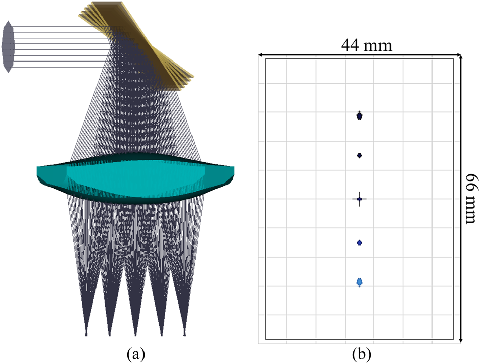
Figure 4. (a) 3D representation of the ray tracing of the designed aspherical telecentric f-θ lens and (b) footprint of the focused rays.
The mirror shown in Fig. 4(a) is tilted at angles of $\pm 20^\circ$ , $\pm 10^\circ$
 , and at $0^\circ$
 , deflecting the beam at twice its tilting angle onto the f-θ lens. The footprint diagram shown in Fig. 4(b) shows the chief ray's incident position for the simulated angles to be $\mp 19.37/$
 mm, $\mp 9.97$
 mm, and 0 mm, respectively.
Besides being diffraction-limited, telecentricity and flat image plane criteria in the new design are evaluated. It is taken into consideration that the beam diameter at all angles is kept constant in different ranges from the radar. The effective and back focal length are EFL = 58.01 mm and BFL = 50 mm, respectively. For performance evaluation and optimization the Rayleigh criteria in optics are taken into account here.
Figure 5 shows the spot diagram on the optical focal plane at five different off- and on-axis scan angles and for all the wavelengths, for a geometrical optics evaluation of the system. The incident ray distributions show signs of other aberrations for the off-axis field points in addition to the spherical aberration on all points.

Figure 5. On- and off-axis spot diagram in the image plane for five scan angles $\pm 20^\circ$ , $\pm 10^\circ$
 , and $0^\circ$
 , without and with Airy disk for comparison.
To compare the aberrations magnitude to limiting effect of diffraction on the lens’ performance, we compare the geometrical spot radius to the Airy radius, the radius of the optical system's response to a point source after diffraction. The maximum and root-mean-square spot radii are R max = 1.032 mm and R rms = 310 μm, respectively, where the Airy radius is R Airy = 5.66 mm. As a result, the geometrical aberrations are negligible and well-suppressed compared to the diffraction.
Of the different numerical methods for modeling optical aberrations, we look at two of them, e.g. the Seidel coefficients and Zernike polynomials. Figure 6 shows the contribution of each lens surface to the aberration coefficients and the accumulated effect of them on the optical image plane. The remaining aberrations are well negligible to the smallest wavelength of 1.7 mm at 174 GHz.
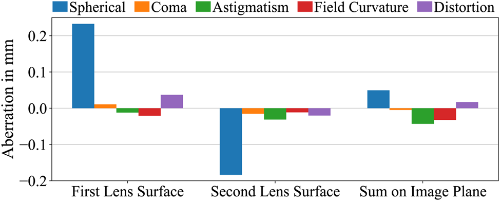
Figure 6. Seidel coefficients on each lens surface and on the image plane.
Zernike polynomials model wavefront error compared to an ideal wavefront in the presence of optical aberrations [Reference Bass, DeCusatis, Enoch, Lakshminarayanan, Li, Macdonald, Mahajan and Van Stryland17]. In a well-designed system W pv < λ/4, where W pv is the peak-to-valley wavefront error in wavelengths, or more strictly W rms < λ/14, with W rms as RMS wavefront error in wavelengths. For the designed f-θ lens the wavefront error at the highest off-axis point gives W pv = 0.019 ≪ λ/4 and W rms = 0.0054 ≪ λ/14, confirming the system to be aberration-free. Lastly, we look at the Strehl ratio, the ratio between peak value of the aberrated image of a point source and the maximum diffraction intensity. When S > 0.8 an optical system is considered to have a good performance. Strehl ratio is calculated from the Zernike polynomials for our lens to be S = 0.999. All the investigated parameters ensure a diffraction-free optical system.
The lateral resolution of the optical system can be found by looking at the cut-off spatial frequency of modulation of the complex optical transfer function (MTF). According to Fig. 7(a), presenting the accumulative MTF functions for all the four for the positive scan angles, the cut-off frequency is ν max ≈ 0.208 cycles/mm, yielding a theoretical lateral resolution of R lateral = 4.8 mm. Moreover, the simulated point spread function (PSF) on the image plane for all wavelengths and over different scan points, Fig. 7(b), shows that the focused beam profile is preserved along the scan line. Here for the sake of simplicity, it is assumed that the signal power is equally distributed over the opening angle for all the rays. It is seen in the PSFs that the signals distribution is kept over the scan range.

Figure 7. (a) MTF and (b) PSF cross-section in the logarithmic scale in tangential (T) and sagittal (S) planes. The simulations are done on the on-axis point with $0^\circ$ deflection, and two off-axis points with $10^\circ$
 and $20^\circ$
 deflection of the radiation.
Finally, we evaluate the system's performance with physical optics, in which the wavefront propagation throughout the optical system is observed, whereas in ray optics the system model is based on rays. We take the signal to be of Gaussian nature to be focused after reflection and refraction through the optical path. Figure 8 shows the Gaussian beam propagated and detected in the image plane for different scan angles, for the minimum and maximum frequencies of 68 and 174 GHz.

Figure 8. Focused Gaussian beam on image plane for $\pm 20^\circ$ , $\pm 10^\circ$
 , and $0^\circ$
 scan angles.
A dynamic range of 10 dB for each row is selected for a high contrast concentrating mainly on the Gaussian beam's mainlobe. In Gaussian optics the beam size is defined as the distance from the axial point where the power drops to 1/e 2 = 0.135 of its maximum value on the axis. This translates into −8.686 dB. This is the reason behind showing a dynamic range of 10 dB here.
We see a relatively well-preserved wavefront and beam waist in the image plane for all the angles. The slight deviation from an ideal case is however due to the smaller aperture of the mirror mounted on the galvoscanner compared to the Gaussian beam size of the radiation. This could be further improved by fixing the aperture matching to avoid apodization of the radiation as much as possible.
System architecture
The preliminary setup for the mobile terahertz FMCW telecentric f-θ scanning system is shown in Fig. 9.

Figure 9. Handheld terahertz FMCW scanning platform.
The required space in the system when using the MMIC radar is decreased significantly in comparison to the bigger dimensions the split-block FMCW unit would need. The mirror has an aperture of 45.5 × 32 mm2 and including the galvanometer mount an overall height of ≈130 mm. Its amplifier board is controlled via an field-programmable gate array-based platform. The mirror can rotate in between $\pm 23,\; \, 377^\circ$ at a maximum speed of $\approx \! 1700^\circ /{\rm s}$
 . Optimized for our setup, it moves $\pm 15^\circ$
 at $\approx \! 50^\circ /{\rm s}$
 . The 3D printed lens is shown in Fig. 10. The printed layers have a thickness of 120 μ m and since this stepped structure of the lens surface is very small compared to the used wavelength, we do not see a relevant influence on the radiation.

Figure 10. Front and back of the 3D printed lens made of PA.
A preliminary inspection of PA for terahertz and sub-terahertz applications showed us that the absorption of PA at frequencies above 450 GHz is significant and therefore, is not suitable for systems with higher operation frequencies.
System evaluation and results
As depicted in Fig. 2, we call the axis perpendicular to the sensor's translational movement, along which the beam is being steered, the scan-axis, and the one on which the sensor unit moves, the motion-axis. To eliminate effects of possible misalignment on the optical path, signal apodization, lens surface roughness, and systematic noise we perform a calibration on the received signal at all the scan points [Reference Schreiner, Sauer-Greff, Urbansky, von Freymann and Friederich3], so that we can achieve homogeneous B- and C-scans. This calibration technique, dividing the sample's signal to a reference signal, normalizes the amplitude of the signal, and the phase center of the IF signal is moved to the reference position as well. Furthermore internal reflections from the optical setup are compensated within the measurement signal by this calibration procedure.
In order to compare the performance of the radars, we first look at the range-gated signal of a metal reflector in the focal plane, and the signal in its absence for noise measurement. Figure 11 shows the amplitude envelope's distribution with frequency for each radar. The effects of the system noise and signal sensitivity drop at the lower and higher parts of the signal's frequency are compensated for with the three-term calibration mentioned in [Reference Schreiner, Sauer-Greff, Urbansky, von Freymann and Friederich3].

Figure 11. Reflected signal from the focal plane in the presence of a metal reflector and in its absence with (a) 80 GHz and (b) 150 GHz radars.
The first evaluation made on the scanner is its performance consistency along the scan- and range-axis. To evaluate the telecentricity performance of the f-θ objective in combination with the MMIC FMCW radar, a test measurement with a metal reflector in the back focal plane is performed. The metal plate is then moved 10 mm toward and farther away from the sensor unit. Figures 12(a) and 12(c) show that the f-θ lens keeps the A-scan profile on the on- and off-axis points in the focal plane consistent to a very good degree, even for angles larger than the optimized value of $\pm 20^\circ$ .
.

Figure 12. A-Scans of a reflector in the image plane at seven positions on the scan line measured with (a) 80 GHz and (c) 150 GHz radars. B-Scans of a reflector in the image plane along scan-axis, and in ± 10 mm of the focal plane measured with (b) 80 GHz and (d) 150 GHz radars.
Moreover, the optical path difference (OPD) to the reflecting plane is equal for all the tilted positions, suggesting a flat focal plane where the scan-line lies. At the edges of the scan axis, however, distortions become dominant and negatively affects the performance, which is shown better in Figs 12(b) and 12(d).
To verify the system's overall performance we performed a 3D imaging on a sample. The flat-bottom hole step-wedged sample made of PE, shown in Fig. 13, has holes of different diameters on each step and its thickness varies from 11 to 15 mm with 1 mm step size. The sample is illuminated from its flat side to look for those hidden features on its back side.

Figure 13. Custom-made stepped-wedge sample of PE material: (a) back view and (b) side view. The dimensions of features and patterns are in mm. The area distinguished within the dashed rectangle roughly shows the scanned area. The steps change from 15 to 11 mm in 1 mm steps. The diameters of the holes increase in each column linearly in steps of 4, 2, and 1 mm, whereas in each row they are halved.
The scanned area is roughly shown in Fig. 13(a). B-scans along the scan-axis and motion-axis are shown in Fig. 14 at different locations. The discontinuities and steps are visible in the cross-sections of the 3D volumetric data of the sample. The flat surface that is the reflection closer to the radar module. We observe that the smaller holes are better resolved in B-scans obtained with the 150 GHz radar. For example in the B-scan on the line y = 88 mm, where three holes of 20, 10, and 5 mm diameter lie, the structure is much better resolved both in transverse and range, with the 150 GHz radar.

Figure 14. B-Scans of the step-wedge sample along the scan- and motion-axes at different positions measured with (a) 80 GHz and (b) 150 GHz radars. The measured step thicknesses, in mm, along the line x = 0 are written in white on the B-scan image. The values match the optical thicknesses according to an index of refraction of approximately 1.54 for PE.
By looking at the C-scans at different depths in Fig. 15, the defects and steps are visible from the top-view as well. Internal hidden defects down to 1 mm are detected with the telecentric f-θ sensor system. Here, telecentricity has kept the location of features constant in different depths of the C-scan.

Figure 15. C-Scans of the step-wedge sample along the scan- and motion-axes acquired using (a) 80 GHz and (b) 150 GHz radars.
By finding the reflection positions from each boundary interface, R 1 and R 2, a 3D model of each surface of the sample is obtained, shown in Fig. 16.

Figure 16. 3D representation of the reflection positions in the volume from the sample's interfaces measured with (a) 80 GHz and (b) 150 GHz MMIC radar units. R 1 represents the reflection range from the first surface facing the radar module, and R 2 determines the reflection ranges from the stepped side of the sample.
Due to the higher bandwidth of the 150 GHz radar, the peaks are better separated, therefore, the steps and holes structures are defined more clear. Also with its radiation at shorter wavelengths compared to the 80 GHz radar, smaller features and holes are better resolved. The optical distance between the two reflections shown in Fig. 17, is equal to the thickness of the sample at each point times material's index of refraction. The change in the sample's thickness due to the stepped structure and holes is distinguished sharper with the 150 GHz module, due to its smaller spot size.

Figure 17. OPD between the two interfaces of the step-wedge sample calculated with the data from (a) 80 GHz and (b) 150 GHz radars.
Here, we see a very well integration of both radars with different carrier frequencies and bands with a single f-θ lens. This provides us with the flexibility to select the proper FMCW radar module based on the sample under test's optical and physical properties, such as refractive index, absorption, thickness, etc. In [Reference Friederich, May, Baccouche, Matheis, Bauer, Jonuscheit, Moor, Denman, Bramble and Savage18], for example, the trade-off of better signal penetration in the W-band versus better resolution in the D-band are exemplified with thick glass fiber reinforced composite structures.
Conclusion
A novel hand-guided mobile terahertz 3D imaging system with a new aspherical telecentric f-θ lens is integrated into a mobile FMCW terahertz imaging platform. In order to allow for a broader scan range, a new f-θ lens with a larger aperture has been designed. To match the aperture of the lens to that of the scanning mirror, the new lens has a rectangular aperture. The lens fabrication is made possible with the SLS 3D printing, where the used material is PA. Two ultra-wideband SiGe-MMIC FMCW radars operating at 80 and 150 GHz are used as transceivers to prove the adaptability of the system to different sub-terahertz frequency bands. We showed here, that the new opto-mechanical scanning system operates well in a wide frequency range of more than 100 GHz, thanks to PA's nearly constant refractive index throughout this frequency range. With the sensor movement along a line, the scanning system acquires a B-scan of the sample on its so-called scan-axis, which is perpendicular to the motion-axis. The lateral resolution of the f-θ lens is kept constant on each point of the scanned line, by preserving the focused beam's size and shape. Depending on the application and the test objects, the platform can easily be adapted to suitable sensors with the appropriate operation frequencies, bandwidths, measurements rates, etc. for any specific imaging scenario.
In future works, we will improve the system to have a faster imaging rate with a proper housing for in-field applications. In order to decrease and eliminate possible chromatic aberrations we intend to inspect the change of refractive index of the lens material throughout an even larger frequency range. Furthermore, it is intended to implement machine learning techniques in our imaging scheme to support automatic detection of anomalies [Reference Bauer, Hussung, Matheis, Reichert, Weichenberger, Beck, Matuschczyk, Jonuscheit and Friederich19, Reference Sharma, Hussung, Keil, Friederich, Fromenteze, Khalily, Deka, Fusco and Yurduseven20].
Financial support
This work was partly funded by the Federal Ministry of Education and Research (grant numbers 16KIS1404 K, 16KIS1405, 16KIS1406); and the Fraunhofer Internal Programmes (grant number SME840104).
Competing interests
The authors report no conflict of interest.
 Shiva Mohammadzadeh was born in Tehran, Iran, in 1989. She received her B.Sc. in electrical engineering – telecommunications, from the University of Tehran in 2012, and her M.Sc. in photonics from Friederich-Schiller University of Jena in Germany in 2016. She joined the group electronic terahertz measurement techniques (ETM) at Fraunhofer Institute for Physical Measurement Techniques IPM in 2015. Since 2017 the group is part of Fraunhofer Institute for Industrial Mathematics ITWM, where she is currently pursuing her Ph.D.. Her field of research includes radar imaging, optical design, electronic and optoelectronics radars, and signal processing.
 Raphael Hussung received Bachelor of Science (B.Sc.) and Master of Science (M.Sc.) in electrical engineering and computer engineering from TU Kaiserslautern, Kaiserslautern, Germany, in 2018 and 2020, respectively. During that time, he worked part time with Pollux Electromechanical Systems GmbH, Kirchheimbolanden, Germany, a supplier of conditioning systems for the automotive industry, where he was tasked with hard- and software development. He joined Fraunhofer Institute for Industrial Mathematics, Kaiserslautern, as a Research Associate, in July 2020. His research interests include millimeter wave and terahertz imaging with multistatic sensor arrays for non-destructive testing applications.
 Andreas Keil was born in Kiel, Germany, in 1975. He graduated in physics from Christian Albrechts University, Kiel, Germany, in 2003, and received his Ph.D. in 2010 from the National University of Singapore, Singapore, in quantum information. From 2009 to 2013, he was involved in the research and development of terahertz imaging systems with SynView GmbH, Bad Homburg, Germany. Since 2013, he has been with Becker Photonik GmbH, Porta Westfalica, Germany, where he continued this line of work, and since 2018 with Fraunhofer ITWM as well. His main research interests include terahertz imaging, image processing algorithms, and high-performance computation on general purpose graphics processing units.
 Sven Leuchs received Bachelor of Science (B.Sc.) in measurement and sensor technologies and Master of Science (M.Sc.) in applied physics from Hochschule Koblenz in 2013 and 2017, respectively. During that time he worked part time as an engineer at the Fraunhofer Institute for High-Frequency Physics and Radar Techniques in Wachtberg in the field of material analysis and development of radar sensors. From 2018 he is the deputy group leader of the Industrialized High-Frequency Technology group in the Department for Integrated Circuit and Sensor Systems (ISS).
 Christian Krebs is group leader for industrial high-frequency technology and deputy department head of the Integrated Circuits and Sensor Systems Department at Fraunhofer FHR. In 2008, he successfully completed his studies in medical technology at the Koblenz University of Applied Sciences with a diploma and supplemented his academic education with business studies, obtaining an MBA in 2022. Since 2010, he has been working at Fraunhofer FHR in the area of material analysis and sensor development, where he and his group are significantly advancing the research in hardware development of highly compact high-frequency sensor systems, multi-channel MIMO systems, and additive manufacturing methods for lenses and integration of power amplifiers.
 Dirk Nüßler received Dipl-Ing. in electrical engineering from the University in Siegen in 1994. In 1995 he joined the Institute for High Frequency Physics and Radar Technique in Wachtberg. He investigated phased array systems and was involved in the development of planar antenna concepts, millimeter wave radar sensors, and Rotman lenses for 100 and 220 GHz. From 2000 to 2005 he joined the workgroup mmW radiometer and was engaged in projects for passive portal and security scanners. In 2005 he started to build a new group for industrial measurement systems. From 2007 to 2016 he was the head of the workgroup “Industrial Measurement Technology,” and since 2009 he is the speaker of the business unit “Production” and since 2017 head of the department for “Integrated Circuits and Sensors.” In 2017, he completed his Ph.D. at the Technical University of Hamburg-Harburg. Since 2020, he has been deputy institute director of Fraunhofer FHR. In the last 25 years he was responsible for more than 30 research projects. He is the author and co-author of more than 90 scientific papers.
 Jörg Seewig studied electrical engineering at the University of Hanover. From 1995 to 1999 he was a scientific assistant in the field of production measurement technology at the Institute for Measurement and Control Technology, University of Hanover. After receiving his Ph.D. (Dr.-Ing.) in 2000 he co-founded an engineering office with focus on software development for production measurement technology. Since 2008, he is full professor and the chairman of the Institute of Measurement and Sensor Technology at the Technical University of Kaiserslautern within the Department of Mechanical and Process Engineering. Furthermore, he is the German delegate in the ISO/TC 213, WG 15 “Filtration” and WG 16 “Surface Texture” and chairman of the mirror committee in DIN. He is the author of various international and national standards in the field “Geometric Product Specification.” Beyond that, he is a partner in Opti-Cal GmbH, since 2018.
 Georg von Freymann graduated in physics from the Universitét Karlsruhe (TH), Karlsruhe, Germany, in 1998 and received his Dr. rer.-nat. in physics from the same institution in 2001. In 2002 he was a PostDoc at the Institute of Nanotechnology at the Forschungszentrum Karlsruhe, Germany. From 2003 to 2004, he was a PostDoc with the University of Toronto, Canada. From 2005 to 2010 he headed an independent DFG Emmy-Noether research group at the Institute of Nanotechnology at the Karlsruhe Institute of Technology (KIT). Since 2010, he is a full professor for experimental physics at the Technische Universitét Kaiserslautern, Germany. Since 2013, he also heads the department Materials Characterization and Testing at the Fraunhofer Institute for Industrial Mathematics ITWM. He is the author of more than 110 articles, and is also involved in more than 15 inventions. He is the co-founder of two companies. His research interests include 3D laser-lithography, nano-photonics, optical quantum simulators, terahertz technology, and spin wave optics.
 Fabian Friederich graduated in optoelectronics at Aalen University Sciences, Germany, in 2007, and received Ph.D. in physics from the Goethe University Frankfurt am Main, Germany, for his work in terahertz imaging with the Ultrafast Spectroscopy and Terahertz Physics Group in 2012. During his studies, he was also associated with the Centre for Micro-Photonics, Swinburne University of Technology, Melbourne, Australia, and with the Laser Zentrum Hannover in Germany. In 2011, he joined the Institute of Technical Physics, German Aerospace Center (DLR), Stuttgart, Germany to establish laser-based concepts for monitoring space debris. In 2013, he was granted a Fraunhofer Attract Funding to form a new research group in the field of millimeter-wave and terahertz measurement techniques at the Fraunhofer Institute for Physical Measurement Techniques IPM. Since 2017, his group has been with the Fraunhofer Institute for Industrial Mathematics ITWM, Kaiserslautern.


 Open access