


Introduction
A key design target for all modern microwave systems is the minimization of their power consumption that means focusing on improving the efficiency of the transmitter, in particular of the power amplifier (PA). However, its achievement is made difficult by the other requirements of these systems, in particular the need to operate at different power levels. This is very relevant when using signals with some form of amplitude modulation, and advanced PA architectures like the Doherty power amplifier [Reference Grebennikov and Bulja1, Reference Camarchia, Pirola, Quaglia, Jee, Cho and Kim2] or outphasing [Reference Barton3] are normally used to address this issues. Envelope tracking has proven to be a powerful technique in maintaining efficiency for high peak-to-average power ratio (PAPR) signals; however, these systems are often highly complex and impose demanding requirements on the DC power supply [Reference Bala, Kazakevich and Yang4]. Furthermore, changing the drain voltage without making corresponding changes to the device loading causes sub-optimal efficiency and additional circuitry is required to modulate the load impedance [Reference Bhardwaj, Moallemi and Kitchen5]. Existing alternatives to ET are able to maintain a constant optimum load by simultaneously reducing input and output bias [Reference Deng, Gudem, Larson, Kimball and Asbeck6, Reference Sahu and Rincon-Mora7] but are generally limited to bipolar technologies.
A slower adaptation of the average or maximum power can also happen in systems, both telecom (traffic adaptation), or in radar and targeting systems to adjust range and accuracy. For these cases, techniques such as slow envelope tracking is likely to be very effective as the requirement for a very fast drain voltage supply is relaxed [Reference He, Ge and Chang8, Reference Asbeck and Popovic9]. On the other hand, most PAs require lowering the input drive when reducing the drain bias voltage to avoid over-driving the transistors into compression, as the load is normally fixed by a passive matching network.
In this work, we propose a new way of maintaining optimum transistor operation by splitting the gate DC bias of a multi-finger transistor so that portions of the active device can be switched OFF when reducing the drain bias, which leads to effective and efficient output power control without need of controlling the input power. This way, the PA can be used almost as an independent block where its output can be controlled simply by changing DC voltages. A PA prototype was designed and measured in K-band to prove the concept. An initial explanation of the split-gate PA and small signal measurements of the PA prototype were presented in [Reference Powell, Quaglia, Powell and Cripps10] at the European Microwave Integrated Circuits Conference 2024. This paper extends that work by providing a thorough explanation of the principles, and by presenting the load–pull characterization of a test-cell to further demonstrate the concepts and understand the limitations of the technique in an experimental way. It also reports the large signal measurements of the PA prototype, fully validating, for the first time, the effectiveness of the technique.
Principle of operation
This paper employs the WIN Semiconductors’ NP12-01 GaN-on-SiC technology targeting mm-wave power applications through 50 GHz. This 0.12 μ m gate process is manufactured on 50 μ m SiC substrates. It uses a source-coupled field plate design to provide the high breakdown voltage required for reliable operation at the drain bias of 28 V, showing a typical saturated output power of 4 W/mm and drain efficiency over 50% at 29 GHz. The NP12-01 platform supports multiple microwave monolithic integrated circuit (MMIC) functions, including optimized switch transistor layouts, two interconnect metal layers, high-reliability metal-insulator-metal (MIM) capacitors, precision TaN resistors, and through-wafer vias for low inductance grounding.
Figure 1 illustrates the archetypal split-gate design, in which the field effect device has two gate pins which are biased to  $V_\mathrm{GG1}$ and $V_\mathrm{GG2}$, the drain is biased to $V_{\mathrm{DD}}$. An RF input must be equally divided between all of the gate sub-busses while keeping DC independence; this can be achieved using a parallel arrangement of DC blocking capacitors and independent bias feed networks. The input RF signal is fed through dual input DC blocking capacitors, while a single DC blocking capacitor is used at the output.
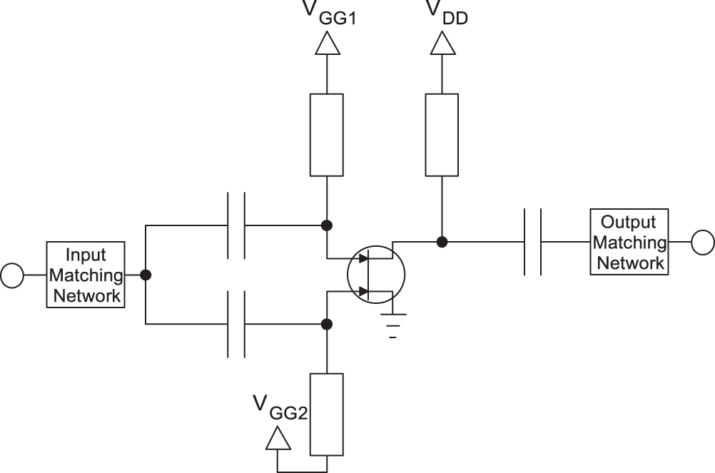
Figure 1. Conceptual circuit diagram of the split-gate.
To improve compactness and lower the chance of asymmetries in the layout due to components’ tolerances, the input matching is placed before the input DC block to avoid duplicating matching elements for each sub-bus.
A trade-off is presented to designers as layout complexity and area increases with the number of DC gate sub-buses. The number of fingers per sub-bus can also be made asymmetrical to provide greater switching action. To simplify the initial implementation, the transistor was split into two, two-finger gate buses of 100 μm length which equates to a single device of 400 μm periphery.
Keeping one sub-bus biased in class AB in all conditions, the other sub-buses can be switched alternately between class-AB and deep class C biases. The deep class C bias should be chosen such that the expected RF input signal cannot produce any RF current at the output, i.e. the gates are fully OFF.
This arrangement is equivalent to reducing the active periphery of the device and therefore its current and subsequently output power.
Other than a system advantage of not having to control the input power, there is also the potential to mitigate efficiency reduction at reduced output power, as by switching OFF part of the transistor also the quiescent current is reduced. What could be perceived as a disadvantage of this technique is that the gain of the device has been reduced as gain is defined by the ratio of output power to input power, but this is an intrinsic consequence of this mode of operation.
The full potential of this technique is achieved when combined with drain bias control. One can examine the DCIV characteristics and the ideal Class B loadline of the device under the “normal” (full ON) operation as in Figure 2(Top).
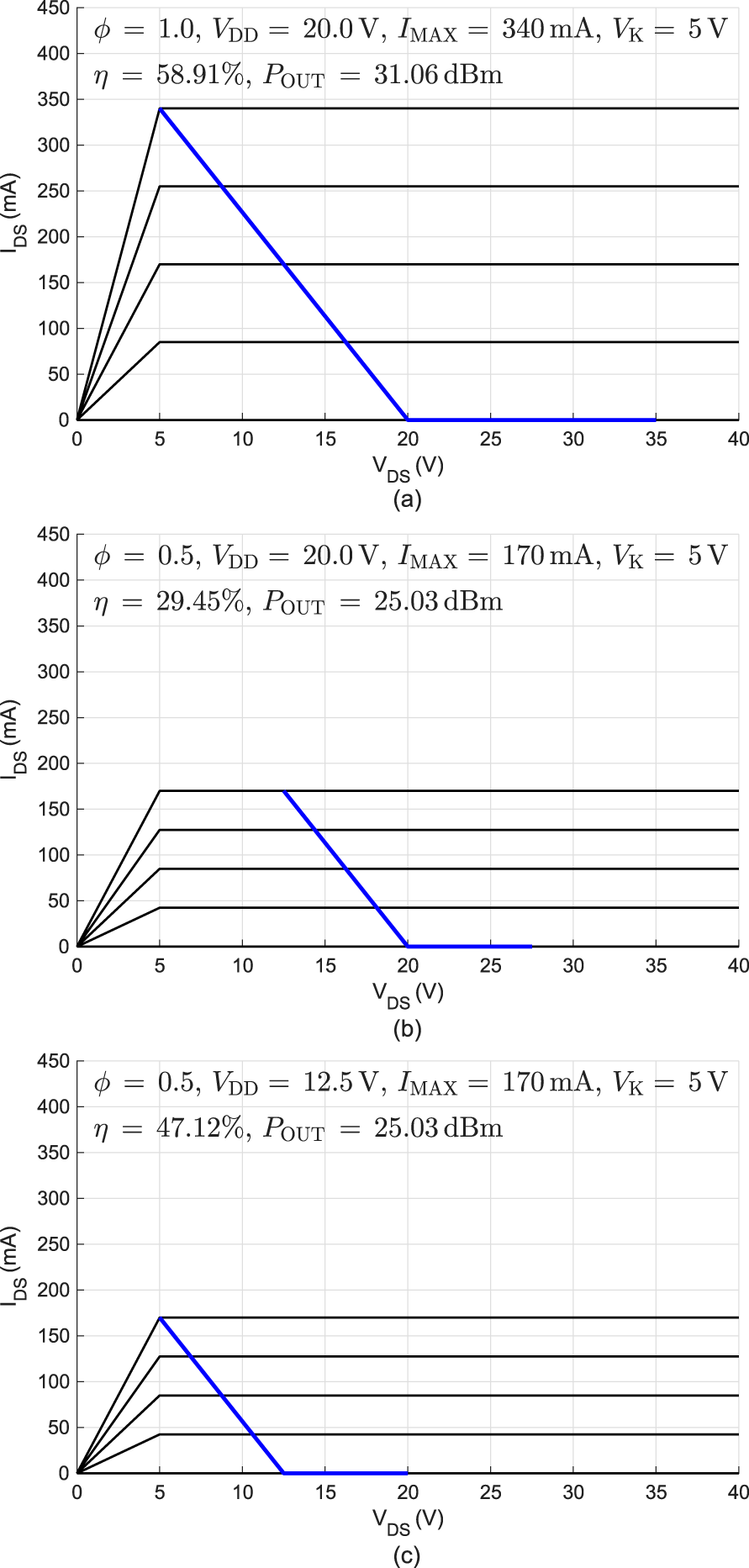
Figure 2. Ideal direct-current current-voltage (DCIV) characteristic and ideal Class B loadline (with fixed fundamental load of ∼85.7 Ω). (Top) 350 mA available drain current  $V_{\mathrm{DD}}$=20 V; (Center) 175 mA available drain current $V_{\mathrm{DD}}$=20 V; (Bottom) 175 mA available drain current $V_{\mathrm{DD}}$=12.5 V.
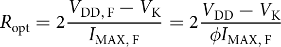
The optimum load of a Class B device can be calculated in equation 1 [Reference Cripps11].
 \begin{equation}
R_\mathrm{opt} = 2\frac{V_{\mathrm{DD}}-V_\mathrm{K}}{I_\mathrm{MAX}} \\
\end{equation}
\begin{equation}
R_\mathrm{opt} = 2\frac{V_{\mathrm{DD}}-V_\mathrm{K}}{I_\mathrm{MAX}} \\
\end{equation} For the optimum load to be restored,  $R_\mathrm{opt}$ must be the same in the full power (denoted with subscript $\mathrm{F}$) and reduced power conditions as in equation 2.
 \begin{equation}
R_\mathrm{opt} =
2\frac{V_\mathrm{DD,\,F}-V_\mathrm{K}}{I_\mathrm{MAX,\,F}} =
2\frac{V_{\mathrm{DD}}-V_\mathrm{K}}{I_\mathrm{MAX}}
\end{equation}
\begin{equation}
R_\mathrm{opt} =
2\frac{V_\mathrm{DD,\,F}-V_\mathrm{K}}{I_\mathrm{MAX,\,F}} =
2\frac{V_{\mathrm{DD}}-V_\mathrm{K}}{I_\mathrm{MAX}}
\end{equation} Let the proportion of active gate fingers be denoted as ϕ and hence (assuming an approximately linear transfer function), the maximum available drain current is  $\phi I_\mathrm{MAX,\,F}$ which can be substituted in equation 2 find the adjusted bias voltage as in equation 5.
 \begin{align*}
R_\mathrm{opt} =
2\frac{V_\mathrm{DD,\,F}-V_\mathrm{K}}{I_\mathrm{MAX,\,F}} &=
2\frac{V_{\mathrm{DD}}-V_\mathrm{K}}{\phi I_\mathrm{MAX,\,F}}
\end{align*}
\begin{align*}
R_\mathrm{opt} =
2\frac{V_\mathrm{DD,\,F}-V_\mathrm{K}}{I_\mathrm{MAX,\,F}} &=
2\frac{V_{\mathrm{DD}}-V_\mathrm{K}}{\phi I_\mathrm{MAX,\,F}}
\end{align*}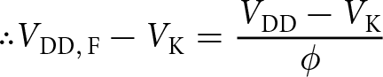 \begin{align*}
\therefore
V_\mathrm{DD,\,F}-V_\mathrm{K} &=
\frac{V_{\mathrm{DD}}-V_\mathrm{K}}{\phi}
\end{align*}
\begin{align*}
\therefore
V_\mathrm{DD,\,F}-V_\mathrm{K} &=
\frac{V_{\mathrm{DD}}-V_\mathrm{K}}{\phi}
\end{align*} \begin{align}
\therefore
V_{\mathrm{DD}} &= \phi (V_\mathrm{DD,\,F}-V_\mathrm{K}) + V_\mathrm{K}
\end{align}
\begin{align}
\therefore
V_{\mathrm{DD}} &= \phi (V_\mathrm{DD,\,F}-V_\mathrm{K}) + V_\mathrm{K}
\end{align}It should be noted that the non-ideal properties of GaN devices such as dispersion [Reference Hirshy, Casbon and Tasker12] and knee walkout [Reference Ubochi, Ahmeda and Kalna13] cause the optimum drain bias reduction to differ from its ideal value. The true optimum reduced gate bias can be found experimentally by conducting a series of power measurements at different drain biases.
Output power reduction
The well-known maximum output power of a Class B device is given in equation 6.
 \begin{equation}
P_\mathrm{OUT,MAX} =
\frac{1}{4}
(V_{\mathrm{DD}}-V_\mathrm{K})
I_\mathrm{MAX}
\end{equation}
\begin{equation}
P_\mathrm{OUT,MAX} =
\frac{1}{4}
(V_{\mathrm{DD}}-V_\mathrm{K})
I_\mathrm{MAX}
\end{equation}Applying equation 5 to equation 6, the reduced output power can be written as in equation 7.
 \begin{equation}
P_\mathrm{OUT,MAX,}{\phi} =
\frac{1}{4}
\left(\phi (V_\mathrm{DD,\,F}-V_\mathrm{K}) \right)
\phi I_\mathrm{MAX,\,F}
\end{equation}
\begin{equation}
P_\mathrm{OUT,MAX,}{\phi} =
\frac{1}{4}
\left(\phi (V_\mathrm{DD,\,F}-V_\mathrm{K}) \right)
\phi I_\mathrm{MAX,\,F}
\end{equation}The full-power condition can be written as in equation 8
 \begin{equation}
P_\mathrm{OUT,MAX,\,F} =
\frac{1}{4}
(V_\mathrm{DD,\,F}-V_\mathrm{K})
I_\mathrm{MAX,\,F}
\end{equation}
\begin{equation}
P_\mathrm{OUT,MAX,\,F} =
\frac{1}{4}
(V_\mathrm{DD,\,F}-V_\mathrm{K})
I_\mathrm{MAX,\,F}
\end{equation}The reduction in output power is therefore the ratio of eqs. 7 and 8 as in equation 9.
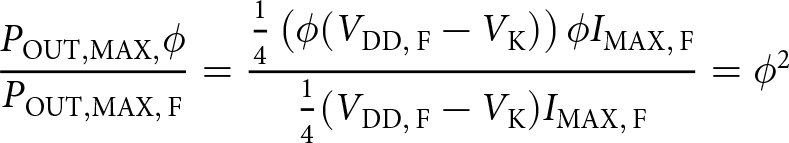 \begin{equation}
\frac{P_\mathrm{OUT,MAX,}{\phi}}{P_\mathrm{OUT,MAX,\,F}}
=
\frac{
\frac{1}{4}
\left(\phi (V_\mathrm{DD,\,F}-V_\mathrm{K}) \right)
\phi I_\mathrm{MAX,\,F}
}{
\frac{1}{4}
(V_\mathrm{DD,\,F}-V_\mathrm{K})
I_\mathrm{MAX,\,F}
} =
\phi^2
\end{equation}
\begin{equation}
\frac{P_\mathrm{OUT,MAX,}{\phi}}{P_\mathrm{OUT,MAX,\,F}}
=
\frac{
\frac{1}{4}
\left(\phi (V_\mathrm{DD,\,F}-V_\mathrm{K}) \right)
\phi I_\mathrm{MAX,\,F}
}{
\frac{1}{4}
(V_\mathrm{DD,\,F}-V_\mathrm{K})
I_\mathrm{MAX,\,F}
} =
\phi^2
\end{equation}Equation 9 indicates that the knee voltage does not impact the power reduction and that the power drops by the square of the fraction of active gate fingers.
The ideal class-B conditions are calculated in Figure 2 has two gate sub-buses hence the power reduction is  $\phi^2 = (0.5)^2=-6.02\,\mathrm{dB}$. Figure 2 shows a power reduction of $31.18\,\mathrm{dBm}-25.16\,\mathrm{dBm}=6.02\,\mathrm{dB}$ as expected for a symmetrical split gate.
Drain efficiency reduction
A similar argument can be made for the drain efficiency as in Section power_reduce using the well-known efficiency expression for Class B devices in equation 10.
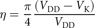 \begin{equation}
\eta
=
\frac{\pi}{4}
\frac{
(V_{\mathrm{DD}}-V_\mathrm{K})
} {
V_{\mathrm{DD}}
}
\end{equation}
\begin{equation}
\eta
=
\frac{\pi}{4}
\frac{
(V_{\mathrm{DD}}-V_\mathrm{K})
} {
V_{\mathrm{DD}}
}
\end{equation}The efficiency reduction can be evaluated as in equation 11.
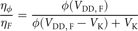 \begin{equation}
\frac{
\eta_\phi
} {
\eta_F
} =
\frac{
\phi (V_\mathrm{DD,\,F})
} {
\phi (V_\mathrm{DD,\,F}-V_\mathrm{K}) + V_\mathrm{K}
}
\end{equation}
\begin{equation}
\frac{
\eta_\phi
} {
\eta_F
} =
\frac{
\phi (V_\mathrm{DD,\,F})
} {
\phi (V_\mathrm{DD,\,F}-V_\mathrm{K}) + V_\mathrm{K}
}
\end{equation}Equation 11 shows that the knee voltage prevents complete efficiency restoration which presents a practical limitation on the selection of ϕ.
The split-gate therefore allows RF systems to dynamically transition between operation in high and low output power states without substantial loss of efficiency. Switching between these two states only requires DC voltage switching which is not resource intensive compared to other techniques.
Split-gate PA design
To demonstrate the split-gate concept, the simplest case of a 2:2 device was designed based on a standard 4×100 μm high-electron-mobility transistor (HEMT) device as in Figure 3.
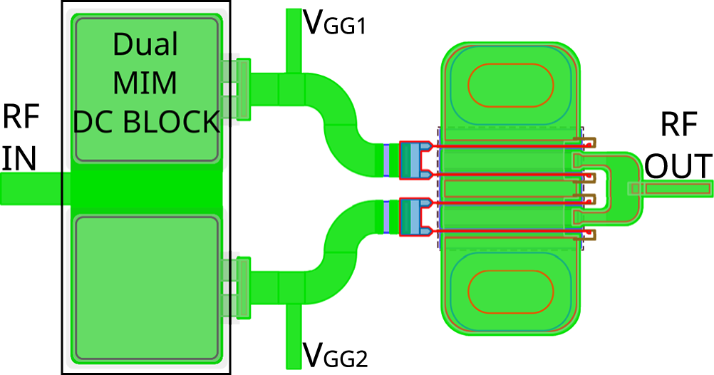
Figure 3. Layout of the split-gate device in Keysight ADS.
A double MIM capacitor was constructed to provide the DC blocks which consisted of a continuous bottom metal layer and two smaller areas of dielectric and top metals which were connected to with air bridges in the conventional way. Thin-film resistors were used to provide in-band stabilization, placed in series with each gate connection.
The full PA was completed by adding input and output matching, output matching (including DC block) and out-of-band stability networks as in Figure 4.
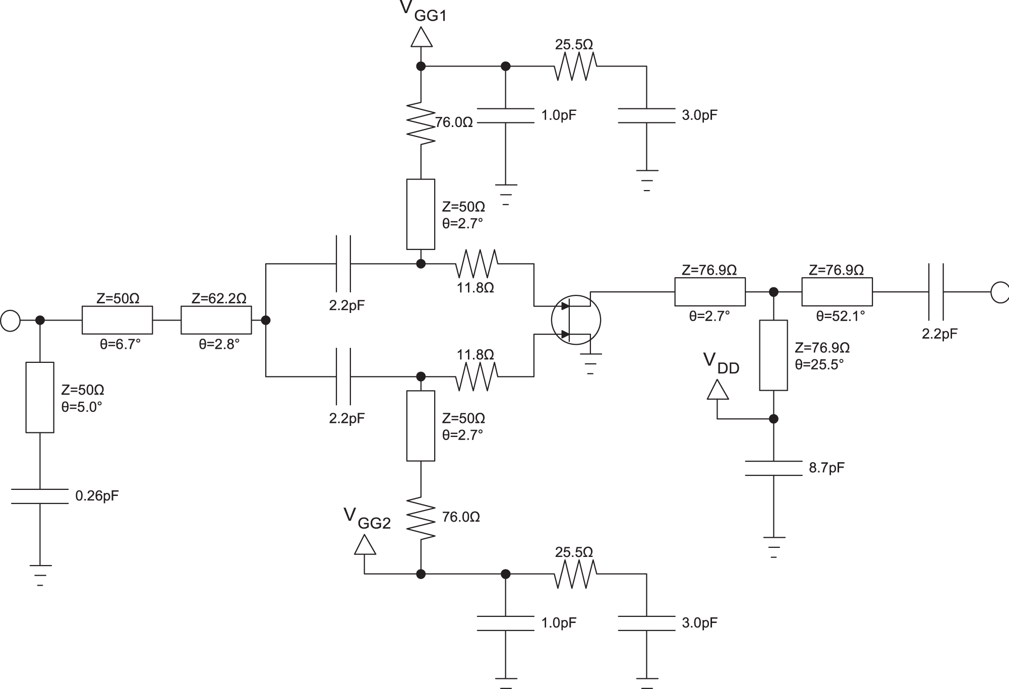
Figure 4. Simplified schematic of the split-gate PA.
The most representative method of simulating the split-gate is to use appropriately sized coplanar waveguide (CPW) device models and external source vias. Unfortunately, the available version of the NP12 PDK did not provide CPW models; therefore, simulations were performed by running two microstrip 2×100 μm models in parallel; load–pull measurements were conducted to characterize the device rather than relying on the 2×100 μ m model which certainly differs from the split-gate device operating in low-power mode.
The NP12 HEMT pinches off at  $V_\mathrm{GG}$ = −2.0 V and was operated in class-AB at 100 mA/mm when fully ON, which means 40 mA for the whole device, and 20 mA when turning OFF half the device.
Fixed matching networks are designed for the ON condition then the biases are changed to match the low-power condition and the simulation is repeated.
A photograph of the fabricated PA is given in Figure 5. The lower gate bias feed has been routed around the RF input pads to facilitate mounting by feeding the DC bias from the top side only.

Figure 5. Photograph of the manufactured split-gate PA die (size  $2\times1.3$ mm2).
Characterization of the split-gate device
The split-gate PA does not allow for measurements at the device plain; therefore, an identical device without matching network was designed and fabricated as in Figure 6 and referred to as split-gate device rather than split-gate PA.
Figure 6. Photograph of the manufactured split-gate device die (size  $1.2\times1.3$ mm2).
DCIV measurements, shown in Figure 7, were conducted on the device using a Keysight B1500A to test the basic functionality. The gate biases were delivered by external wires and the drain bias was delivered using a 150 μm wafer probe.
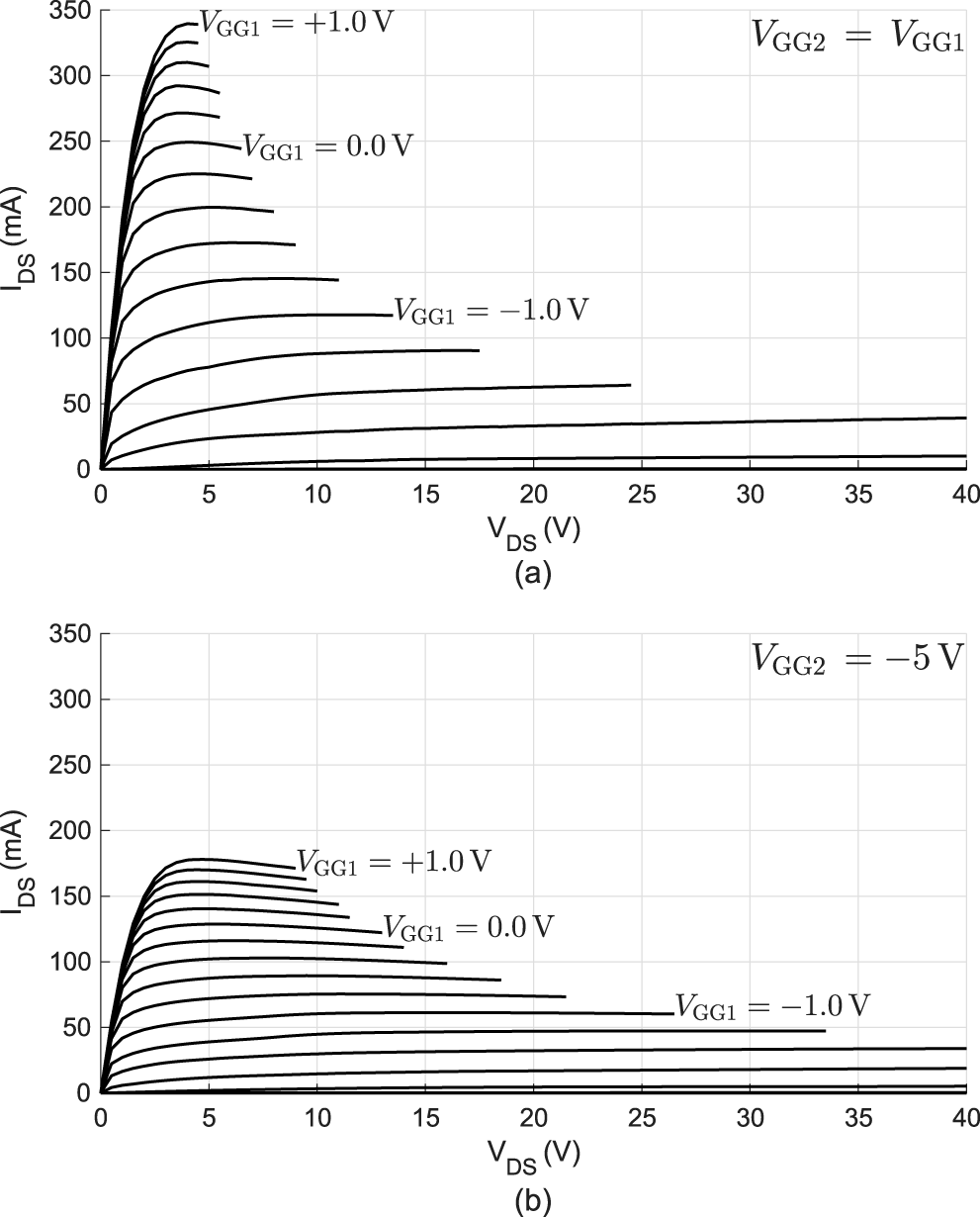
Figure 7. DCIV measurements with all gates active (Top) and half of the gates active (Bottom) from  $V_\mathrm{GG1}\,=\,-3.6\,\mathrm{V}$ to $+1.0\,\mathrm{V}$.
The gate wires were connected together to emulate the high-power condition in Figure 7(Top) and one of the gate wires was connected to a fixed  $-5\,\mathrm{V}$ supply in Figure 7(Bottom) to emulate the low-power condition.
Figure 7 shows that the split-gate current halves as expected confirming the DC functionality of the split-gate.
Load–pull measurements were conducted at 17 GHz to verify the consistency between optimum loads in high- and low-power modes, which were  $22 + \mathrm{j}56 \,\Omega$ and $18 + \mathrm{j}47 \,\Omega$, respectively, as in Figure 9; the movement of $4 + \mathrm{j}9 \,\Omega$ allows the designer to choose a compromise between these impedances. The frequency of the load–pull does not match that of the design as it was selected for convenience as a better driver PA was available for 17 GHz to drive the unmatched device during load–pull. However, the frequencies are close enough so that we could consider the test relevant.
The large-signal measurement system used to characterize the split-gate (see Figure 8) is a source-load–pull, based on a vector network analyzer (67 GHz PNA-X from Keysight). The “Delta” tuners from Focus Microwave are directly connected to the probes, minimizing insertion loss and enabling the measurements at high reflection coefficients ( $|{\Gamma}|$ values up to 0.85). For this measurement, a fundamental-only load–pull was conducted, with harmonics and source impedances terminated at the system impedance ( $50\,\Omega$) by the tuner.
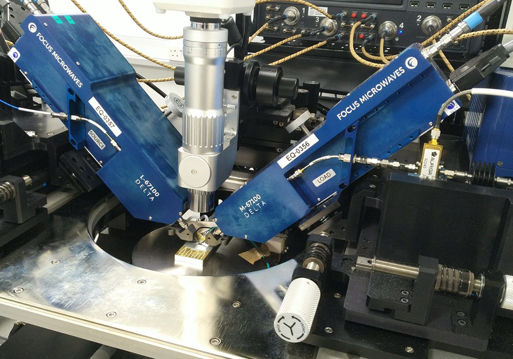
Figure 8. Photograph of the split-gate in the load–pull system.
Observing Figure 9, it is clear that the optimum loads under low- and high-power conditions have approximately the same impedance. The residual difference in optimum loads can be attributed to the properties of GaN devices such knee walkout [Reference Ubochi, Ahmeda and Kalna13], dispersion [Reference Hirshy, Casbon and Tasker12] and the drain varactor effect [Reference Beleniotis, Schnieder, Krause, Haque and Rudolph14].
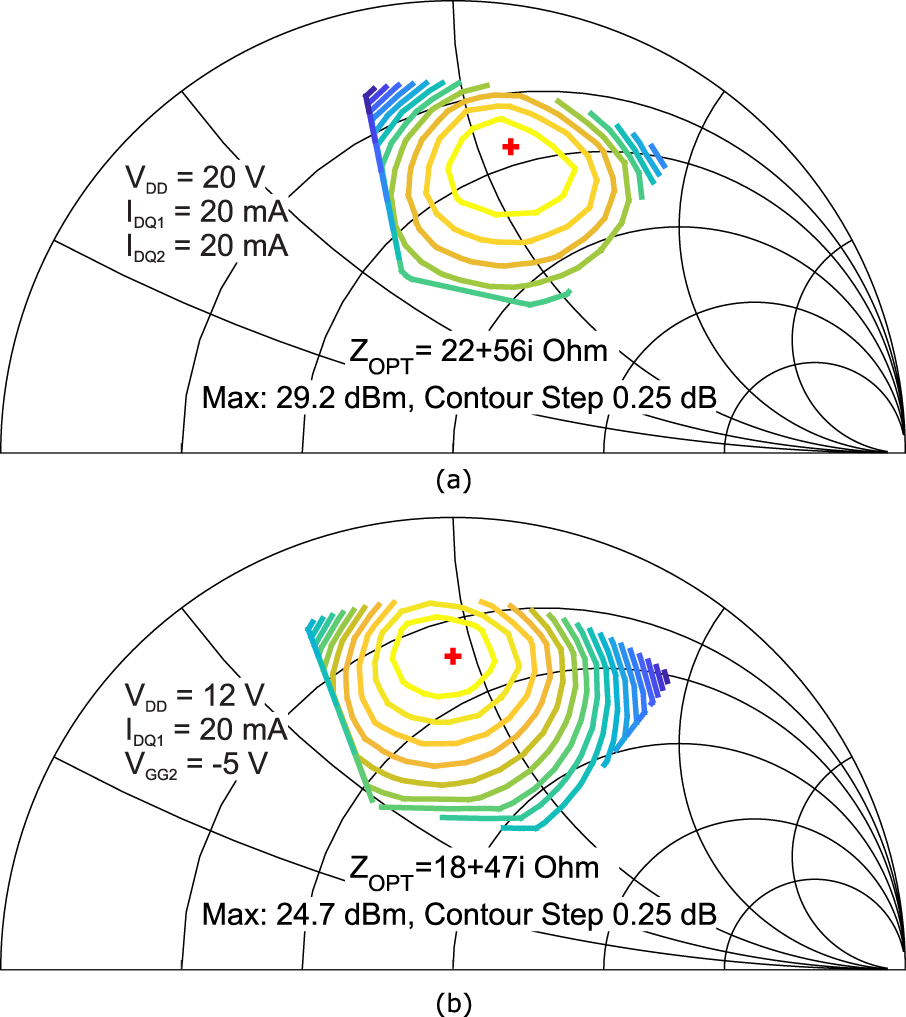
Figure 9. Power contours of split-gate device under 20 V drain bias with all gates active (Top) and 12 V with half of the gates active (Bottom).
Figure 10 shows the drain efficiency contours, indicating that the efficiency would not substantially change if the device were loaded at the power optimum for the high power mode as per a fixed matching network.
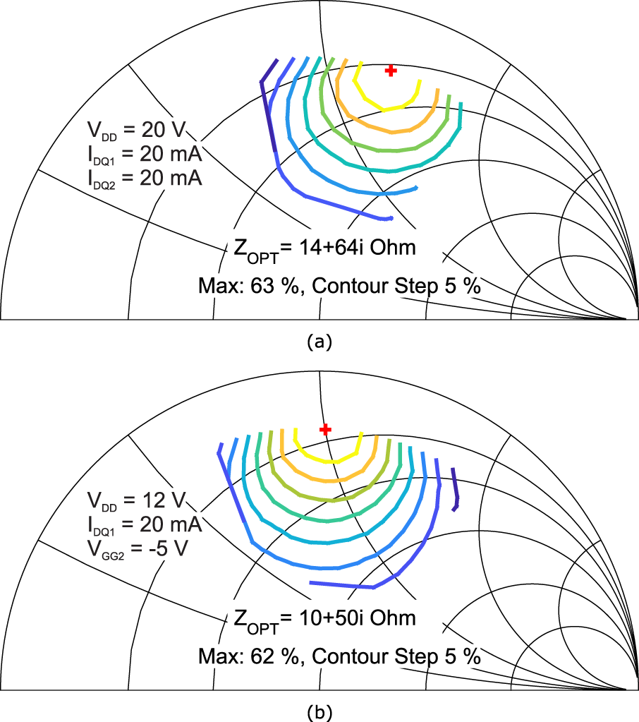
Figure 10. Drain efficiency contours under 20 V drain bias with all gates active (Top) and 12 V with half of the gates active (Bottom).
Split-gate PA characterization
Small-signal measurements
Small signal measurements were conducted using drain bias voltages of 12 and 20 V with various gate biases. The input and output matching are reported in Figure 11. The measurement show some frequency shift, of 500–700 MHz toward lower frequencies. Imperfections in the matching contribute to the gain being lower than expected which can be seen in Figure 12, but the measurements and simulations appear to be close in frequency. The maximum frequency of the amplifier is reduced from 24.6 GHz in simulation to 23.5 GHz in measurement.
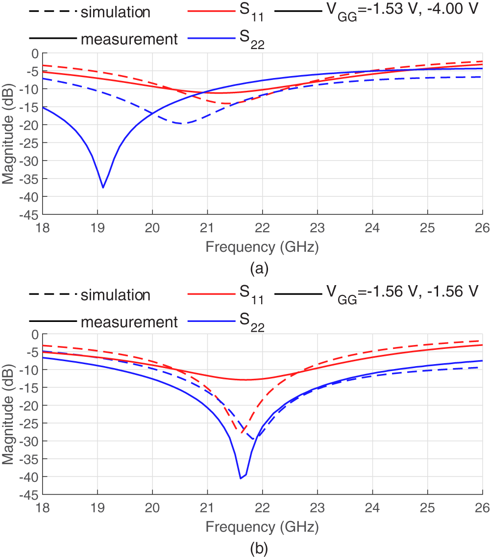
Figure 11. Measured reflective s-parameters of split-gate under (a) 12 V and (b) 20 V drain biases.
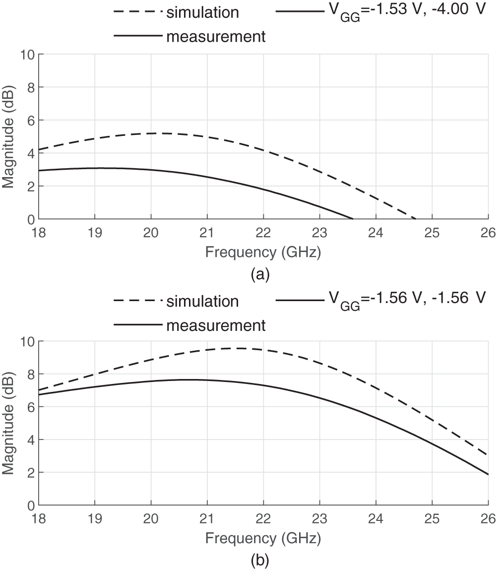
Figure 12. Measured transmission s-parameters of split-gate under (a) 12 V and (b) 20 V drain biases.
Depending on the technology, the change in gate and drain bias can have a significant effect on the input and output capacitance leading to a change in the frequency response. Inevitably a designer must choose some compromise between optimum performance over the domain of variables, i.e. gain and power tunability, maximum power and gain, and bandwidth.
Power measurements
The power measurements were conducted using a ZVA67 by Rohde & Schwarz. The system was calibrated to the probe tips. The large signal measurements are shown at the frequency of 22 GHz.
By controlling the gate voltage only, the maximum output power can be reduced from 28.4 to  $24.7\,\mathrm{dBm}$, while reducing the drain voltage causes a further reduction to $23.2\,\mathrm{dBm}$ as in Figure 13.

Figure 13. Measured output power vs input power for various bias conditions.
The efficiency restoration can be seen in Figure 14, where gate control alone causes a notable drop in efficiency (down to 22%), which is restored when the drain voltage is also dropped (back to  $\simeq$ 30%).
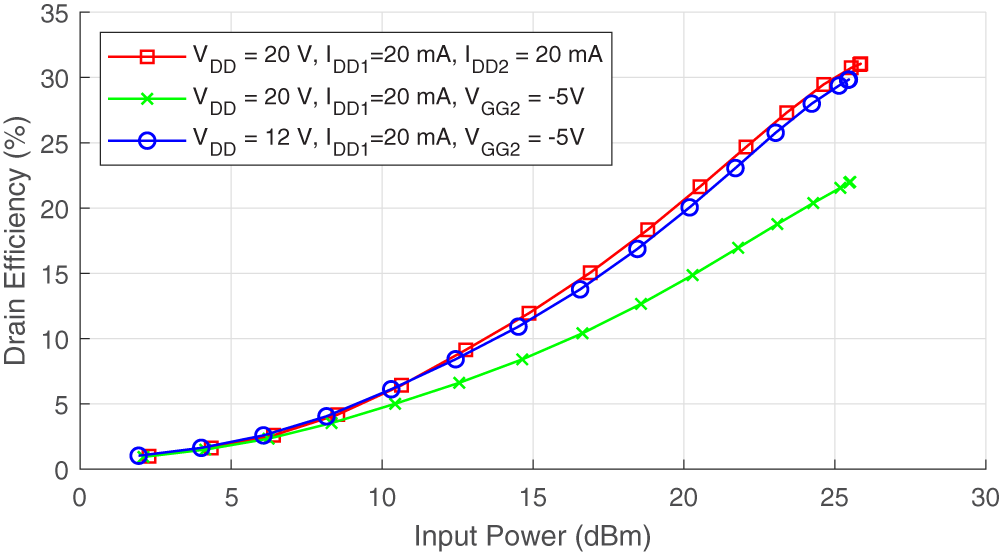
Figure 14. Measured drain efficiency vs input power for various bias conditions.
Figure 15 shows the measured power gain which shows the expected reduction of around 4.8–4.9 dB consistently across the power sweep. The compression also appears more pronounced when the number of gates was reduced but the drain bias voltage was unchanged, as it would be expected due to non-optimal loading.
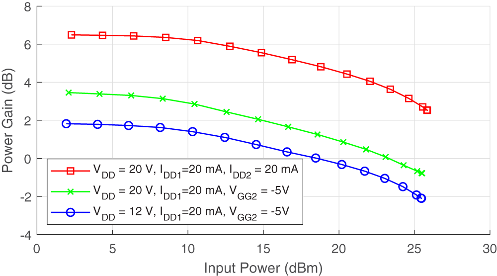
Figure 15. Measured power gain vs input power for various bias conditions.
Practical implementations of the split-gate can use constant input power; however, it is illustrative to examine device performance with respect to output power hence drain efficiency and gain are given again in Figures 16 and 17, respectively.
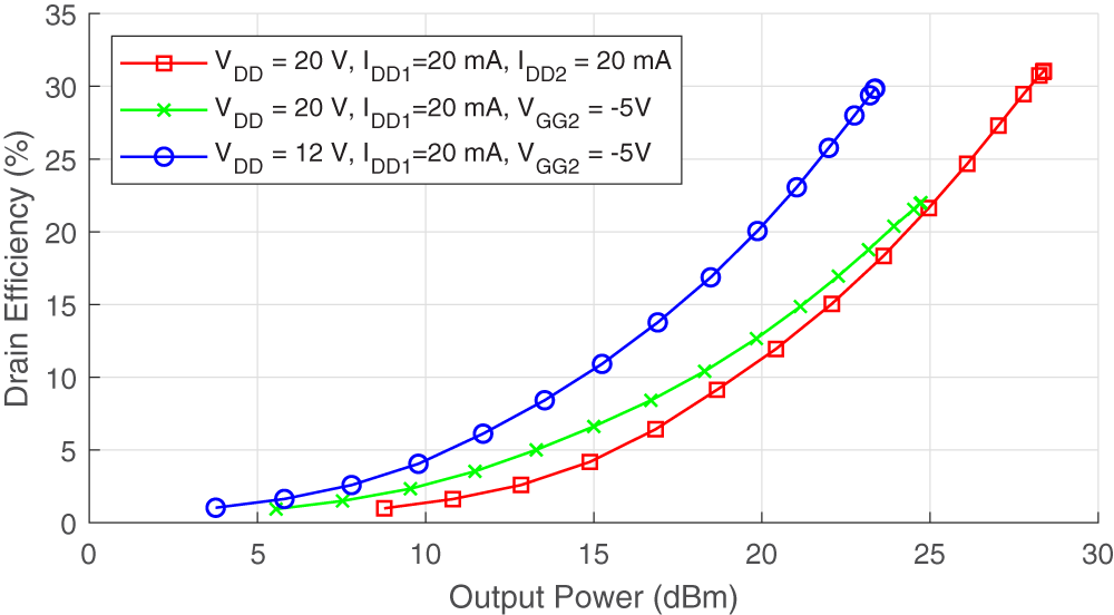
Figure 16. Measured drain efficiency vs output power for various bias conditions.
Power measurements were not presented in [Reference Powell, Quaglia, Powell and Cripps10] because the split-gate PA exhibited parametric oscillation in the hundreds of MHz range which was resolved using an off-chip RC network.
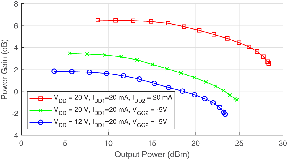
Figure 17. Measured gain vs output power for various bias conditions.
Conclusion
This paper has proposed and demonstrated a conveniently controllable method of modulating device performance in terms of output power and gain while maintaining good efficiency. The theoretical concept has been verified with power and load–pull measurements in a full PA and unmatched device, respectively.
The technique modifies the multi-finger transistor and, with minimal external circuitry, provides a method of virtually reducing the active periphery of a device in real-time. By simultaneously switching the gate and drain bias condition, which can be in principle provided by switching a single DC voltage, the device operates optimally when matched with a fixed load and driven by a fixed average input drive.
The split-gate technique has the potential to be expanded to greater control ranges and enables configuration on the device level rather than the circuit level which could lead to reconfigurability in highly compact MMIC designs. Operating as a variable driver stage, for example, may be extremely useful as discrete power level switching can be achieved with minimal area cost and a traditional fixed interstage matching network can be used to connect to the high-power stage.
Compared to more complex techniques which provide a continuous range over which the system can be optimized, the split-gate provides an alternative which can be optimized for discrete conditions.
Acknowledgements
The authors would like to thank Leonardo for their support of this project and WIN Semiconductors Corp. for fabricating the MMICs.
Competing interests
The authors declare none.

Roberto Quaglia was born in Casale Monferrato, Italy, in 1984. He received the Ph.D. degree in electronic devices from Politecnico di Turin, Turin, Italy, in 2012. He is currently a Senior Lecturer with the School of Engineering, Cardiff University, Cardiff, U.K. His research interests include concern the design, modeling, and predistortion of high-efficiency MMIC power amplifiers. Dr. Quaglia received the European Union Marie Skodowska Curie Fellowship in 2015, the 2009 Young Graduated Research Fellowship presented by the GAAS Association, and the 2024 IEEE Microwave Magazine Best Paper Award. He is the Deputy Chair of the IEEE MTT-TC 12.

Ehsan M. Azad received the bachelor’s degree in petroleum engineering from the University of Gachsaran, Gachsaran, Iran, in 2012, the Doctor of Philosophy degree in electronics from Cardiff and Vale College, Cardiff, U.K., in 2018, and the M.Sc. degree in wireless and microwave communication engineering and the Ph.D. degree in efficiency improvement of base station PAs from the Centre for High Frequency Engineering (CHFE), Cardiff University, Cardiff, in 2019 and 2023, respectively. Since October 2022, he has been with Compound Semiconductor Applications (CSA) Catapult, Newport, U.K., contributing to collaborative projects focused on the development of millimeter-wave PAs. His research interests include various areas, including high-efficiency PAs, with a particular emphasis on Doherty PAs, nonlinear device characterization and modeling, PA linearization techniques, and advanced packaging solutions.

Jeff Powell received the B.Sc. and Ph.D. degrees from the University of Birmingham, Birmingham, U.K., in 1992 and 1995, respectively. Following graduation he continued working at the University of Birmingham, where he investigated properties of ferroelectric and superconducting materials at microwave frequencies. From 2001 to 2010, he was a Principal Engineer with Qineti Q, where he performed many MMIC circuit, hybrid, and module designs for many applications from 2 to 110 GHz using a wide range of commercial and research-based circuit and packaging technologies. In 2010, he formed Skyarna Ltd, Halesowan, West Midlands, U.K., design consultancy that specializes in the design of leading edge circuits; including wideband high-efficiency amplifiers and active circuits to 300 GHz. He has contributed to more than 50 journal and conference publications and also 2 patent applications.

Steve Cripps obtained his master’s and Ph.D. degrees from Cambridge University in the 1970s. After working for several years with the pioneering gallium arsenide (GaAs) group at Plessey Research, he emigrated to the U.S., where he worked for 15 years in various engineering and management positions at Watkins Johnson, Loral, and Celeritek. In 1996 Dr. Cripps returned to the UK, working as an independent consultant before taking on an academic post at Cardiff University, where he is currently a distinguished research professor. Dr. Cripps has authored several best-selling books on RFPA design and is a regular contributor to the IEEE Microwave Magazine with his popular “Microwave Bytes” column. Dr. Cripps is an IEEE Fellow was the 2008 recipient of the IEEE Microwave Application Award.

Aquila Gardiner Powell was born in Leeds, England in 1998. He received the M.Eng. degree in electrical and electronic engineering from the University of Leeds in 2021 and received the M.Sc. degree in compound semiconductor engineering in 2022 from Cardiff University. He is currently working on the Ph.D. with the Centre for High Frequency Engineering at Cardiff University.


 Open access