


Introduction
The fifth-generation cellular networks (5G) enforce stringent requirements on the spectral purity of wireless signals. As such, the transmit signal must typically have a minimum adjacent-channel-power-ratio (ACPR) of −45 dBc [1]. Therefore, 5G transmitters (TX) target nominal ACPR levels of −50 dBc. To achieve such a level with an energy-efficient power amplifier (PA), cellular base station transmitters employ a correction loop consisting of a directional coupler, filter, attenuator, down-converting observation receiver, and a digital pre-distorter unit (Figure 1(a)).
To allow accurate determination of the TX nonlinearities at these large ACPR levels, the down-converting path in such a TX setup must offer at least 60 dBc spurious-free dynamic range (SFDR) to the ADCs, with 3× or 5× the bandwidth of the modulated TX signal (to include the IM3 and IM5 products). To achieve this, practical TX observation loops take a fraction of the TX output signal using a directional coupler. Filtering is applied before the mixer to avoid unintended down-conversion of the harmonic content in the TX signal to the baseband by the harmonics of the mixer LO. Next, high attenuation occurs before the mixer to relax the mixer linearity requirements. The mixer is usually implemented in the current-domain to limit the voltage swings on its intermediate nodes increasing linearity. However, doing so requires linear-IF amplification after the mixer core to drive the capacitive input of the ADC (C in ∼ 0.15 pF) with sufficient voltage swing (e.g., up to 0.2 V). These later requirements combined with 60 dBc SFDR translate to an OIP3 of the observation receiver of 7 dBv or 20 dBm when referred to a 50 Ω load. The linear-IF amplification (e.g., a trans-impedance-amplifier (TIA) following the mixer core) becomes more challenging and power-hungry with increasing modulation bandwidths. More specifically, in sub-6 GHz 5G systems, the transmitter modulation bandwidth can reach 400 MHz, which yields 200 MHz in-phase and quadrature-phase signal representations. However, since the observation receiver also needs to include the IM3 and IM5 products, its actual bandwidth must approach 1 GHz, making the linearity, bandwidth, and power consumption of the observation receiver more and more a concern.
In this work, by introducing a new passive voltage-domain mixer topology capable of providing very high OIP3 and large IF bandwidth and harmonic rejection (HR), we aim to drastically simplify the topology of an observation receiver and avoid the need for power-hungry wideband linear-IF amplification. Moreover, the need for a directional coupler, filter, and attenuator can also be omitted when adequately addressed in the down-converting mixer design. Additionally, when aiming for co-integrating of the proposed mixer with a digital transmitter [Reference Beikmirza2, Reference Bootsman3], the clock generation can be shared (Figure 1(b)). This observation receiver configuration makes classical mixer performance parameters like IIP3 and conversion loss rather arbitrary since they entirely depend on the applied attenuation in the correction loop. Furthermore, since the correction loop aims to model the PA transfer function rather than monitor the TX signal itself, the noisecontributions of the observation receiver are averaged out over time, relaxing the mixer noise figure requirement. Moreover, since filtering in Figure 1(b) is omitted, HR needs to be included in the mixer. Finally, since base station transmitters typically use an isolator in their output, a simple capacitive voltage divider with  $C_\mathrm{2}$ $\gg$
$\gg$  $C_\mathrm{1}$, as shown in Figure 1(b), can be used to simplify the hardware configuration and allow co-integration with the transmitter.
Figure 1. Block diagram of a transmitter with an observation receiver containing the down-converting mixer and a digital pre-distorter (DPD) unit for an (a) analog intensive transmitter and (b) envisioned digital intensive transmitter.
HR in mixers is typically achieved by using multiple sub-mixers in parallel with phase-shifted LO clocks and scaled currents for their switching cores [Reference Weldon4]. This approach allows the mimicking of an N-sampled sinewave LO [Reference El-Aassar5]. These current-domain mixers mostly employ TIAs in their RF and/or IF path, which is one of the causes that their in-band linearity is typically limited to <10 dBm in terms of IIP3 [Reference Pini6–Reference Wang and Guo10]. To date, HR voltage-domain mixers in sub-6 GHz bands have been demonstrated with an OIP3 up to 13 dBm [Reference Kibaroglu12]. Here, OIP3 is the fairer metric to compare, given the conversion loss. In these voltage-domain mixers, the limiting factor for the linearity is the variation of the on-resistance (Ron) of the mixer switches, due to their dependence on the gate-to-source (VGS) voltages, which fluctuate with the RF input signal [Reference El-Aassar5, Reference Kibaroglu12]. In addition, both current and voltage-domain-type mixers using TIAs are restricted by IF bandwidth limitations [Reference Pini6–Reference Wang and Guo10].
To overcome the above challenges, we propose a new voltage-domain passive HR mixer topology for observation receiver applications in which the gate-to-source voltages (VGS) of mixer switches’ always remain constant to achieve high OIP3. Furthermore, by properly designing and scaling the mixer branches while using eight LO phases with a 25% duty cycle, the input impedance of the proposed mixer switching core can be kept constant throughout all LO phases, further boosting its linearity. Finally, the proposed mixer core provides low IF output impedance, allowing the direct wideband handling of capacitive loading by subsequent “I” and “Q” ADCs without any intermediate gain stage and, thus, lower power consumption.
Proposed voltage-domain mixer
Mixer concept
The concept of the proposed voltage-domain mixer can be understood best by considering the simplified schematic of Figure 2(a), representing a single mixer branch with, for now, a virtual ground connected to the node IFout. Only one of the resistor branches is active (contributing current to IFout) at any of the eight LO phases (Figure 2(a)). In this simplified topology, resistors  $R_\mathrm{1}$, $R_\mathrm{2}$, and $R_\mathrm{3}$ are sized such that the current flowing from IFout to the virtual ground, resulting from an activated branch with resistors $R_\mathrm{1}$ and $R_\mathrm{2}$, is a factor $1 + \sqrt{2}$ lower than that of an activated branch with resistors $R_\mathrm{1}$ and $R_\mathrm{3}$, thereby implementing the scaling for HR of the LO waveform (see Figure 2(b)). The proposed configuration benefits from all switches having a well-defined VGS referenced to ground. Therefore, avoiding undesired $R_\mathrm{on}$ modulation due to the RF input or IF output signals, yielding a strongly improved linearity.
Figure 2. (a) Simplified topology and related LO phases; (b) effective harmonic-reject LO waveform; (c) full proposed voltage-domain mixer topology (I-only); (d) eight-phase 25% duty cycle LO waveforms; (e) extended  $I/Q$ mixer topology.
The mixer in Figure 2(a) avoids both RF and LO feed-through to the IF port, as it effectively constitutes a double-balanced mixer (the right-hand side of the schematic in Figure 2(a) uses 180∘ rotated phases for both the RF and LO clock signals compared to the left-hand side). However, IFout is a current summation node; therefore, any common-mode error appearing on the RF or LO ports will directly couple to the IF. To remedy that, the mixer topology is duplicated while flipping the polarity of the RF inputs to arrive at the final proposed mixer topology, shown in Figure 2(c). The resulting differential outputs IFIp and IFIn are now free of both differential as well as common-mode RF and LO input signals. Additionally, they provide a convenient differential signal to drive the subsequent ADC stages. Furthermore, since the use of different duty cycles to drive the switches (as in Figure 2(a)) is problematic in practical circuit implementations, it is beneficial to maintain the same 25% duty cycle across all clocking phases, yielding better phase synchronization between the different clock-paths and, thus, better linearity and HR. This requires splitting each of the two switches controlled by ΦA and ΦB in the simplified topology of Figure 2(a), into three separate switches controlled by 25% duty cycle LO signals Φ1,3,6 and Φ2,5,7 respectively (see Figure 2(d)).
To obtain useful representations of the IF output signals, the virtual ground in the simplified topology needs to be replaced. The most trivial way to do so is to introduce TIAs at these positions. However, practical TIAs will introduce linearity, bandwidth, and power-budget constraints. Since in our observation receiver the mixer conversion gain is not a concern, and all RF and LO signals are already canceled at the IF port, we can remove the virtual ground and use the network terminals IFIp and IFIn directly as the output nodes (Figure 2(c)). With this change, the signals are now all in the voltage-domain. Doing so, resistors  $R_\mathrm{1}$, $R_\mathrm{2}$, and $R_\mathrm{3}$ need to be re-sized to include the IF port impedance in order to maintain the proper HR ratios of Figure 2(b). The effect of the IF port impedance will be further analyzed in “Theory and derivations” section.
The extension to a differential quadrature down-conversion mixer is achieved by duplicating the mixer core topology once more and phase-shifting the LO by 90∘ (Figure 2(e)). The loading of the input nodes RF+ and RF− by the total I/Q mixer now remains perfectly constant throughout all phases of the LO cycle (thus vs. time), again contributing to the linearity of the proposed mixer.
Clock generation
Figure 3 shows a block diagram of the implemented on-chip clock generation chain. A single-ended 50% duty cycle LO clock at frequency 4 ${\times}f_\mathrm{LO}$ is fed to the chip. An on-chip balun designed as a double-tuned transformer is implemented to produce differential LO signals. A phase-aligner and two consecutive divide-by-2 stages are implemented to generate eight-phase 50% duty cycle LO clocks at $f_\mathrm{LO}$. The clock dividers are implemented using D-Latches in a C2MOS (clocked CMOS) topology [Reference Rabaey13]. AND/OR gates devised solely from symmetric NAND gates are then implemented to create eight-phase 25% duty cycle LO waveforms at $f_\mathrm{LO}$. Consequent phase-aligning stages are implemented for better phase synchronization. Buffers are implemented as needed throughout the clocking chain and are not explicitly shown in this block diagram.
Figure 3. (a) Block diagram of the implemented on-chip clock generation chain; (b) from left to right: (i) input 14 GHz clock, (ii) intermediate 7 GHz clock phases after first divider, (iii) intermediate 3.5 GHz clock phases after second divider, (iv) final 3.5 GHz clock phases after 25% duty cycle generation.
Theory and derivations
Input impedance
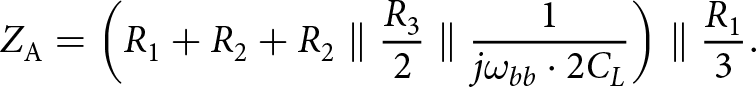
The extension of the proposed mixer topology to an I/Q mixer, as shown in Figure 2(e), has the extra advantage of keeping the input impedance of the total I/Q mixer constant across time. This can be deduced by considering the input impedance of the I and Q mixers during each of the eight LO clock phases. Figure 4 showcases both the I and Q mixers including the IF port’s capacitive load during the first (or fourth) LO clock phase ( $\Phi_\mathrm{A}$ in Figure 2(a)) as an example, from the four branches in the I mixer connecting the RF inputs (RF+ and RF−) to the in-phase IF output (IFIp), only one branch is conducting. Similarly, only one branch of the four branches in the I mixer connecting the RF inputs (RF+ and RF−) to the out-phase IF output (IFIn) is conducting. This holds for every other LO clock phase (see Figure 2(a)), where the one conducting branch in the I mixer swaps between a branch that includes $R_\mathrm{2}$ (as in Figure 4) or a branch that includes $R_\mathrm{3}$. Thus, the input impedance of the I mixer (and similarly the Q mixer) is always switching between two levels that are determined by whether a branch including $R_\mathrm{2}$ or a branch including $R_\mathrm{3}$ is conducting in each of the eight LO clock phases for the I and Q mixer, alongside the related shunt resistances and capacitive load at the IF port. These two impedance levels are coined $Z_\mathrm{A}$ and $Z_\mathrm{B}$. During a single clock phase, when the I mixer has a branch conducting that includes R 2, the Q mixer will have a branch conducting that includes R 3 (as can be seen in Figure 4) and vice versa.
Figure 4. Circuit diagram including IF port capacitive load during first LO clock phase for the (a) I mixer and (b) Q mixer.
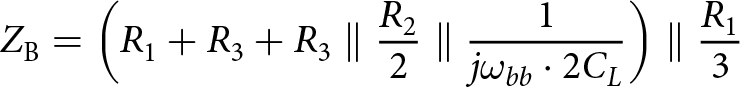
This impedance behavior is visualized in Figure 5 across one full LO cycle. For the I mixer, the single-ended input impedance seen by the RF inputs (RF+ or RF−) across one LO cycle is shown in Figure 5(a) and 5(b), respectively. This shows that the input impedance of the I mixer alone will not be constant and will vary with a period half of that of the LO, providing even-order harmonic content that would limit the mixer’s linearity. For the Q mixer, the single-ended input impedance seen by the RF inputs (RF+ or RF−) across one LO cycle is shown in Figure 5(c) and 5(d), respectively. The total input impedance of the proposed I/Q mixer is, therefore, the parallel combination of the input impedance of the I and Q mixers and is shown in Figure 5(e) and 5(f). This combined input impedance is constant across time and thus boosts the mixer’s linearity. This result only holds in an I/Q mixer with eight LO clock phases. Thus, an I/Q mixer with more LO clock phases (i.e., more samples per LO cycle following the proposed concept) will not have a constant input impedance across time.
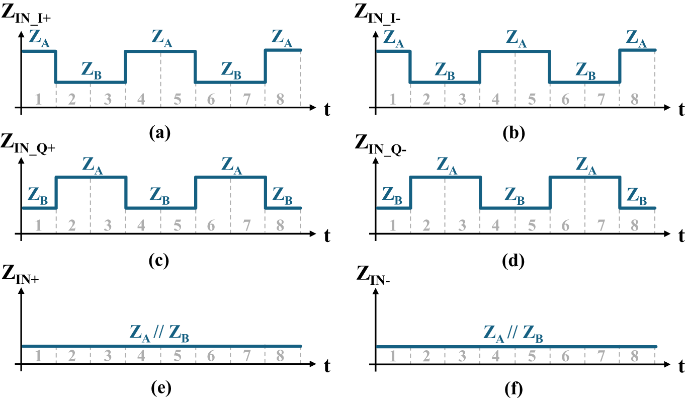
Figure 5. (a) I mixer RF+ single-ended input impedance; (b) I mixer RF− single-ended input impedance; (c) Q mixer RF+ single-ended input impedance; (d) Q mixer RF− single-ended input impedance; (e) I/Q mixer RF+ single-ended input impedance; (d) I/Q mixer RF− single-ended input impedance.
To derive the I/Q mixer’s total input impedance, we need to determine the two impedance levels  $Z_\mathrm{A}$ and $Z_\mathrm{B}$. The impedance $Z_\mathrm{A}$ is the impedance seen by RF+ during the first, fourth, fifth, and eighth phases of the LO, which by design is a single conducting branch with $R_\mathrm{2}$ and three off branches and can be written as:
 \begin{equation}
Z_\mathrm{A} = \left( R_{1} + R_{2} + R_{2} \parallel \frac{R_{3}}{2} \parallel \frac{1}{j\omega_{bb} \cdot 2C_{L}} \right) \parallel \frac{R_{1}}{3}.
\end{equation}
\begin{equation}
Z_\mathrm{A} = \left( R_{1} + R_{2} + R_{2} \parallel \frac{R_{3}}{2} \parallel \frac{1}{j\omega_{bb} \cdot 2C_{L}} \right) \parallel \frac{R_{1}}{3}.
\end{equation} Similarly, the impedance  $Z_\mathrm{B}$ can be derived as the impedance seen by RF+ during the second, third, sixth, and seventh phases of the LO, which by design is a single conducting branch with $R_\mathrm{3}$ and three off branches and can be written as:
 \begin{equation}
Z_\mathrm{B} = \left( R_{1} + R_{3} + R_{3} \parallel \frac{R_{2}}{2} \parallel \frac{1}{j\omega_{bb}\cdot 2C_{L}} \right) \parallel \frac{R_{1}}{3}
\end{equation}
\begin{equation}
Z_\mathrm{B} = \left( R_{1} + R_{3} + R_{3} \parallel \frac{R_{2}}{2} \parallel \frac{1}{j\omega_{bb}\cdot 2C_{L}} \right) \parallel \frac{R_{1}}{3}
\end{equation} where the frequency term  $\omega_{bb} = \, \mid\omega_{\mathrm{rf}} - \omega_\mathrm{lo}\mid$ translates the baseband impedance to the LO frequency due to the mixing action of the switches.
The total constant RF single-ended input impedance of the overall I/Q mixer is the parallel combination of  $Z_\mathrm{A}$ and $Z_\mathrm{B}$ (as visualized in Figure 5(e) and 5(f)). Substituting $Z_\mathrm{A}$ and $Z_\mathrm{B}$ with their derived expressions from (1) and (2), respectively, we can write the total constant single-ended RF input impedance of the overall I/Q mixer seen by RF+ or RF− with respect to ground as:
 \begin{align}
{Z_\mathrm{in}} &= \left( {{R_1} + {R_2} + {R_2}\parallel\frac{{R_3}}{2}} \parallel \frac{1}{j\omega_{bb}\cdot 2C_{L}} \right) \nonumber\\
&\quad \times \parallel \left( {{R_1} + {R_3} + {R_3}\parallel\frac{{R_2}}{2}} \parallel \frac{1}{j\omega_{bb}\cdot 2C_{L}} \right)\parallel \frac{{{R_1}}}{6}.
\end{align}
\begin{align}
{Z_\mathrm{in}} &= \left( {{R_1} + {R_2} + {R_2}\parallel\frac{{R_3}}{2}} \parallel \frac{1}{j\omega_{bb}\cdot 2C_{L}} \right) \nonumber\\
&\quad \times \parallel \left( {{R_1} + {R_3} + {R_3}\parallel\frac{{R_2}}{2}} \parallel \frac{1}{j\omega_{bb}\cdot 2C_{L}} \right)\parallel \frac{{{R_1}}}{6}.
\end{align} Figure 6 plots the mixer’s single-ended input impedance versus input RF frequency using the resistor values provided in Figure 2 and  $C_\mathrm{L} = 150\,\text{fF}$. The calculated mixer’s single-ended input impedance from (3) matches well with the simulated results using ideal switches, where the small deviation between the two curves is due to the steady-state approximation taken in (1) and (2), which was used to simplify the derivation, especially since the input impedance in (3) is dominated by the $\frac{{{R_1}}}{6}$ term from the six “off” branches, significantly reducing the effect of the error due to this approximation. Furthermore, in an observation receiver application, the goal is to have a high enough mixer’s input impedance to avoid significantly loading the PA, thus, an exact derivation is not necessary. The simulated mixer’s input impedance decreases when using real switches due to the extra on-resistance and the off-capacitance, it decreases slightly more at higher RF frequencies mainly due to the off-capacitance.
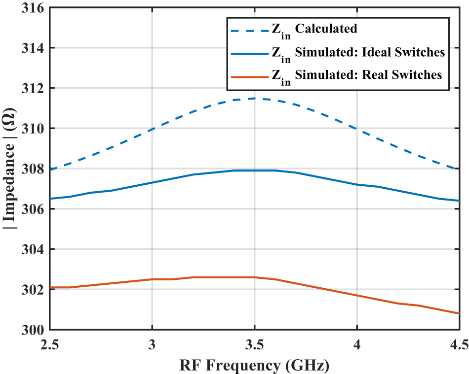
Figure 6. Mixer’s single-ended input impedance.
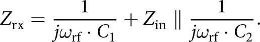
Referring back to the digital intensive transmitter envisioned in Figure 1, the total single-ended input impedance seen looking into the observation receiver path can be written as:
 \begin{equation}
Z_\mathrm{rx} = \frac{1}{j\omega_\mathrm{rf}\cdot C_{1}} + Z_\mathrm{in} \parallel \frac{1}{j\omega_\mathrm{rf}\cdot C_{2}}.
\end{equation}
\begin{equation}
Z_\mathrm{rx} = \frac{1}{j\omega_\mathrm{rf}\cdot C_{1}} + Z_\mathrm{in} \parallel \frac{1}{j\omega_\mathrm{rf}\cdot C_{2}}.
\end{equation} Maximizing this input impedance can be achieved by minimizing  $C_\mathrm{1}$. Assuming $C_\mathrm{1}$ = 10 fF and taking $Z_\mathrm{in} \approx 302\,\Omega$ from Figure 6, it can be directly calculated that $C_\mathrm{2} = 195\,\text{fF}$ is needed to achieve sufficient attenuation from 28 Vp to 1.1 Vp. For a PA with 28 Vp and 50 W peak output power (as in Figure 1), a load impedance of $\approx 8\,\Omega$ is needed. Substituting by the aforementioned values in (3), $Z_\mathrm{rx}$ changes the impedance seen by the PA to $7.9996 \Omega - j\,0.014 \Omega$. A change so minuscule that it should not affect the efficiency of the PA. Furthermore, the matching network can be tuned slightly to account for this shift in the impedance seen by the PA. Finally, with a 1.1 Vp singled-ended input signal to the mixer and $Z_\mathrm{in} \approx 302\,{\Omega}$, the total input RF power drawn by the mixer from both the RF+ and RF− terminals is equal to 4 mW, a value too minuscule (compared to the total PA peak output power) to cause any significant degradation of the transmitter’s system efficiency.
Output impedance
In the observation receiver line-up shown in Figure 1(b), the down-conversion mixer is followed by an ADC, which presents a capacitive load to the down-conversion mixer outputs. Thus, the IF output impedance of the down-conversion mixer needs to be low enough to allow a large IF bandwidth.
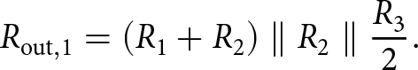
The instantaneous output impedance of either the I or Q mixer varies with time between two values depending on which of the two unique branches is conducting in each of the eight phases of the LO (similar to how the input impedance of either the I or Q mixer varied with time in Figure 5). To derive the mixer’s output impedance, we need to determine these two alternating values of the output impedance. The single-ended output impedance looking into one of the output nodes in Figure 2(c) when a branch that includes  $R_\mathrm{2}$ is conducting and all the other branches are not can be written as:
 \begin{equation}
R_\mathrm{out,1} = \left( R_{1} + R_{2} \right) \parallel R_{2} \parallel \frac{R_{3}}{2}.
\end{equation}
\begin{equation}
R_\mathrm{out,1} = \left( R_{1} + R_{2} \right) \parallel R_{2} \parallel \frac{R_{3}}{2}.
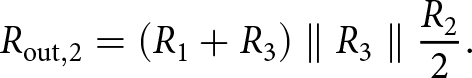
\end{equation} Similarly, the single-ended output impedance looking into one of the output nodes in Figure 2(c) when a branch that includes  $R_\mathrm{3}$ is conducting and all the other branches are not can be written as:
 \begin{equation}
R_\mathrm{out,2} = \left( R_{1} + R_{3} \right) \parallel R_{3} \parallel \frac{R_{2}}{2}.
\end{equation}
\begin{equation}
R_\mathrm{out,2} = \left( R_{1} + R_{3} \right) \parallel R_{3} \parallel \frac{R_{2}}{2}.
\end{equation} The instantaneous output impedance of the mixer is alternating between the two impedance values (5) and (6) with the same frequency as that shown in Figure 5, namely 2 ${\times}f_\mathrm{LO}$. In the intended down-conversion observation receiver application, the IF output is at a much smaller baseband frequency than the LO. As such, we can approximate the mixer’s baseband output impedance as the average between two impedance values in (5) and (6). This averaged output impedance determines the mixer’s baseband output impedance and, therefore, determines the mixer’s baseband bandwidth. The total differential baseband output impedance of either the I or Q mixer is:
 \begin{equation}
R_{{{out}}} \approx \left(\left(R_\mathrm{1} + R_\mathrm{2}\right)\parallel R{\textrm{2}}\parallel\frac{R_{{3}}}{2}\right) + \left(\left(R_\mathrm{1} + R_\mathrm{3}\right)\parallel R_{{3}}\parallel\frac{R_{\textrm{2}}}{2}\right).
\end{equation}
\begin{equation}
R_{{{out}}} \approx \left(\left(R_\mathrm{1} + R_\mathrm{2}\right)\parallel R{\textrm{2}}\parallel\frac{R_{{3}}}{2}\right) + \left(\left(R_\mathrm{1} + R_\mathrm{3}\right)\parallel R_{{3}}\parallel\frac{R_{\textrm{2}}}{2}\right).
\end{equation}The IF bandwidth can then be simply defined as:
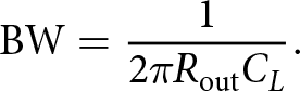 \begin{equation}
\mathrm{BW} = \frac{1}{2\pi R_\mathrm{out}C_{L}}.
\end{equation}
\begin{equation}
\mathrm{BW} = \frac{1}{2\pi R_\mathrm{out}C_{L}}.
\end{equation}Conversion loss
The IF output of the mixer is the result of the multiplication of the RF input with the fundamental component of the LO waveform. Assuming a single-tone RF input with an amplitude of one, the conversion loss of the total mixer is then directly equal to the magnitude of the fundamental component of the effective LO waveform shown in Figure 2(b). To determine that magnitude, we can decompose the effective LO waveform into four separate waveforms shown in Figure 7(a), where the duty cycle of each waveform is exactly 12.5%. The amplitude of the four waveforms is set by the two resistive scaling ratios  $TF_\mathrm{1}$ and $TF_\mathrm{2}$ and depends on the eight phases of the effective LO waveform. For simplicity, the IF port capacitive loading will only be included in the succeeding subsections. $TF_\mathrm{1}$ represents the voltage transfer function from the RF inputs to one of the IF outputs in Figure 4 when a branch including $R_\mathrm{2}$ is conducting and can be written as:
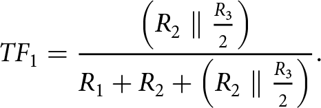 \begin{equation}
{TF_1} = \frac{{\left( {{R_2}\parallel {\textstyle{{{R_3}} \over 2}}} \right)}}{{{R_1} + {R_2} + \left( {{R_2}\parallel {\textstyle{{{R_3}} \over 2}}} \right)}}.
\end{equation}
\begin{equation}
{TF_1} = \frac{{\left( {{R_2}\parallel {\textstyle{{{R_3}} \over 2}}} \right)}}{{{R_1} + {R_2} + \left( {{R_2}\parallel {\textstyle{{{R_3}} \over 2}}} \right)}}.
\end{equation} Similarly,  $TF_\mathrm{2}$ represents the voltage transfer function from the RF inputs to one of the IF outputs in Figure 4 if a branch including $R_\mathrm{3}$ is conducting and can be written as:
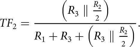 \begin{equation}
{TF_2} = \frac{{\left( {{R_3}\parallel {\textstyle{{{R_2}} \over 2}}} \right)}}{{{R_1} + {R_3} + \left( {{R_3}\parallel {\textstyle{{{R_2}} \over 2}}} \right)}}.
\end{equation}
\begin{equation}
{TF_2} = \frac{{\left( {{R_3}\parallel {\textstyle{{{R_2}} \over 2}}} \right)}}{{{R_1} + {R_3} + \left( {{R_3}\parallel {\textstyle{{{R_2}} \over 2}}} \right)}}.
\end{equation}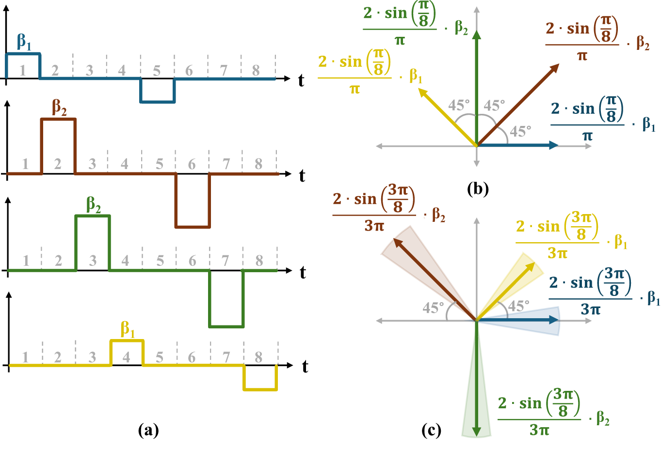
Figure 7. (a) Decomposed LO waveforms; (b) vector representation of the fundamental component of the decomposed LO waveforms; (c) vector representation of the third harmonic of the decomposed LO waveforms with phase error.
All of the decomposed LO waveforms in Figure 7(a) are of 12.5% duty cycle, thus, applying Fourier transform would yield a fundamental coefficient of  $2 \cdot {\sin\left(\frac{\pi}{8}\right)}/{\pi}$. Consequently, the vector representation of the fundamental components of the four decomposed LO waveforms is shown in Figure 7(b). Finally, to derive the fundamental component of the effective LO, we preform a vector summation of the fundamental components of the decomposed waveforms. Thus, the magnitude of the conversion loss can be written as:
 \begin{equation}
{A_L} = \frac{{{\alpha _1}\cdot\left( {{R_2}\parallel {\textstyle{{{R_3}} \over 2}}} \right)}}{{{R_1} + {R_2} + \left( {{R_2}\parallel {\textstyle{{{R_3}} \over 2}}} \right)}} + \frac{{{\alpha _2}\cdot\left( {{R_3}\parallel {\textstyle{{{R_2}} \over 2}}} \right)}}{{{R_1} + {R_3} + \left( {{R_3}\parallel {\textstyle{{{R_2}} \over 2}}} \right)}}
\end{equation}
\begin{equation}
{A_L} = \frac{{{\alpha _1}\cdot\left( {{R_2}\parallel {\textstyle{{{R_3}} \over 2}}} \right)}}{{{R_1} + {R_2} + \left( {{R_2}\parallel {\textstyle{{{R_3}} \over 2}}} \right)}} + \frac{{{\alpha _2}\cdot\left( {{R_3}\parallel {\textstyle{{{R_2}} \over 2}}} \right)}}{{{R_1} + {R_3} + \left( {{R_3}\parallel {\textstyle{{{R_2}} \over 2}}} \right)}}
\end{equation} where α 1 and α 2 are equal to 0.1865 and  ${\sqrt 2 }/{\pi}$, respectively.
The blue curves in Figure 8 show the result calculated from (11) perfectly matching the mixer’s simulated conversion loss without the capacitive load and with ideal switches. The mixer displays no frequency dependence yet due to not including the capacitive load.
Figure 8. Mixer’s conversion loss.
Switch parasitics
To ease the precise clocking of the entire mixer core, all the switches used in the mixer are identical and are sized as shown in Figure 2(c), with dummy switches added to equalize the capacitive load seen by each clock line. The switches need to be sized big enough such that their on-resistances ( $R_{\mathrm{on}}$) acts as an effective “short” to ground for the off branches when the switch is turned on but should also not be over-sized as a bigger switch adds a higher off-capacitance ( $C_{\mathrm{off}}$) which would affect the branches HR performance. In TSMC 40 nm technology, the selected switch with $W_{\mathrm{g}} =$ 13.8 µm and $L_{\mathrm{g}} =$ 100 nm has an on-resistance of 50 Ω and an off-capacitance of 5 fF. The reasoning for not using minimum gate length in the switches is to reduce channel length modulation with drain voltage variation which would introduce a secondary source of nonlinearity. This is highlighted in Figure 9, where the OIP3 improves by increasing the switches’ channel length (while keeping $W_{\mathrm{g}}$/ $L_{\mathrm{g}}$ constant to maintain the same $R_{\mathrm{on}}$) until the effect of the larger off-capacitance added by the larger switches start to dominate.
Figure 9. Mixer’s OIP3 vs. switches’ channel length (constant  $W_{\mathrm{g}}$/ $L_{\mathrm{g}}$).
So far, the parasitic on-resistance and off-capacitance of the switches have been neglected in the above derivations of the mixer, since their effect is mostly secondary. The on-resistance of the switch should be small compared to the values of  $R_\mathrm{1}$, $R_\mathrm{2}$, and $R_\mathrm{3}$. However, as previously stated, the parasitic off-capacitance can have some impact on the previously equated mixer performance parameters.
For the output impedance, we are only interested in the effective baseband impedance so the parasitic off-capacitance can be neglected. For the input impedance, the parasitic off-capacitance can play a role as we’re interested in the RF impedance; however, from (3), we can see that the input impedance is mainly dominated by  $R_\mathrm{1}$ from the six branches that are “off”, thus the effect of the parasitic off-capacitance is also negligible for the input impedance.
The conversion loss will be the most affected by the parasitic off-capacitance as it affects the transfer functions of the two mixer branches at the fundamental carrier frequency ( $f_\mathrm{LO}$). Furthermore, the effect of the IF port loading capacitor $C_\mathrm{L}$ must also be included.
To determine the branch transfer function while including the effect of the capacitances, it is convenient to use two transfer functions. The first transfer function ( $TF_\mathrm{A}$) is the transfer from one of the RF input ports to one of the intermediate mixing nodes $IF_\mathrm{p{\_} A:D}$ and $IF_\mathrm{n{\_} A:D}$ as defined in Figure 2(c). The second transfer function ( $TF_\mathrm{B}$) is the transfer from one of the intermediate mixing nodes $IF_\mathrm{p{\_} A:D}$ and $IF_\mathrm{n{\_} A:D}$ to one of the IF output summation nodes $IF_\mathrm{p}$ and $IF_\mathrm{n}$ as defined in Figure 2(c). It is important to note that the mixing has already occurred at the intermediate mixing nodes $IF_\mathrm{p{\_} A:D}$ and $IF_\mathrm{n{\_} A:D}$, meaning the scaled IF components are already created. Thus, only the baseband frequency is of interest in $TF_\mathrm{B}$. $TF_\mathrm{A}$ including the effect of the capacitances can thus be written as:
 \begin{equation}
{TF_\mathrm{A1}} = \frac{\left({{{R_2} + {R_2}\parallel {\frac{R_3}{2}} \parallel \frac{1}{j\omega_\mathrm{rf}\cdot C_L}} }\right) \parallel \left(\frac{1}{j\omega_\mathrm{rf}\cdot3C_{\mathrm{off}}}\right)}{{{R_1} + \left({{{R_2} + {R_2}\parallel {\frac{R_3}{2}} \parallel \frac{1}{j\omega_\mathrm{rf}\cdot C_L}} }\right) \parallel \left(\frac{1}{j\omega_\mathrm{rf}\cdot3C_{\mathrm{off}}}\right)}}
\end{equation}
\begin{equation}
{TF_\mathrm{A1}} = \frac{\left({{{R_2} + {R_2}\parallel {\frac{R_3}{2}} \parallel \frac{1}{j\omega_\mathrm{rf}\cdot C_L}} }\right) \parallel \left(\frac{1}{j\omega_\mathrm{rf}\cdot3C_{\mathrm{off}}}\right)}{{{R_1} + \left({{{R_2} + {R_2}\parallel {\frac{R_3}{2}} \parallel \frac{1}{j\omega_\mathrm{rf}\cdot C_L}} }\right) \parallel \left(\frac{1}{j\omega_\mathrm{rf}\cdot3C_{\mathrm{off}}}\right)}}
\end{equation} \begin{equation}
{TF_\mathrm{A2}} = \frac{\left({{{R_3} + {R_3}\parallel {\frac{R_2}{2}} \parallel \frac{1}{j\omega_\mathrm{rf}\cdot C_L}} }\right) \parallel \left(\frac{1}{j\omega_\mathrm{rf}\cdot C_{\mathrm{off}}}\right)}{{{R_1} + \left({{{R_3} + {R_3}\parallel {\frac{R_2}{2}} \parallel \frac{1}{j\omega_\mathrm{rf}\cdot C_L}} }\right) \parallel \left(\frac{1}{j\omega_\mathrm{rf}\cdot C_{\mathrm{off}}}\right)}}
\end{equation}
\begin{equation}
{TF_\mathrm{A2}} = \frac{\left({{{R_3} + {R_3}\parallel {\frac{R_2}{2}} \parallel \frac{1}{j\omega_\mathrm{rf}\cdot C_L}} }\right) \parallel \left(\frac{1}{j\omega_\mathrm{rf}\cdot C_{\mathrm{off}}}\right)}{{{R_1} + \left({{{R_3} + {R_3}\parallel {\frac{R_2}{2}} \parallel \frac{1}{j\omega_\mathrm{rf}\cdot C_L}} }\right) \parallel \left(\frac{1}{j\omega_\mathrm{rf}\cdot C_{\mathrm{off}}}\right)}}
\end{equation} where  $TF_{\mathrm{A1}}$ and $TF_{\mathrm{A2}}$ denote $TF_{\mathrm{A}}$ in a conducting branch including $R_\mathrm{2}$ and $R_\mathrm{3}$ respectively.
Similarly,  $TF_{\mathrm{B1}}$ can be written as:
 \begin{equation}
{TF_\mathrm{B1}} = \frac{{\left( {{R_2}\parallel {\textstyle{{{R_3}} \over 2}} \parallel {\frac{1}{j\omega_{bb}\cdot C_L}}} \right) \parallel{\frac{1}{j\omega_{bb}\cdot 3C_{\mathrm{off}}}} }}{{{R_2} + \left( {{R_2}\parallel {\textstyle{{{R_3}} \over 2}}} \parallel {\frac{1}{j\omega_{bb}\cdot C_L}} \right)} \parallel{\frac{1}{j\omega_{bb}\cdot 3C_{\mathrm{off}}}} }
\end{equation}
\begin{equation}
{TF_\mathrm{B1}} = \frac{{\left( {{R_2}\parallel {\textstyle{{{R_3}} \over 2}} \parallel {\frac{1}{j\omega_{bb}\cdot C_L}}} \right) \parallel{\frac{1}{j\omega_{bb}\cdot 3C_{\mathrm{off}}}} }}{{{R_2} + \left( {{R_2}\parallel {\textstyle{{{R_3}} \over 2}}} \parallel {\frac{1}{j\omega_{bb}\cdot C_L}} \right)} \parallel{\frac{1}{j\omega_{bb}\cdot 3C_{\mathrm{off}}}} }
\end{equation} \begin{equation}
{TF_\mathrm{B2}} = \frac{{\left( {{R_3}\parallel {\textstyle{{{R_2}} \over 2}} \parallel {\frac{1}{j\omega_{bb}\cdot C_L}}} \right) \parallel{\frac{1}{j\omega_{bb}\cdot C_{\mathrm{off}}}} }}{{{R_3} + \left( {{R_3}\parallel {\textstyle{{{R_2}} \over 2}}} \parallel {\frac{1}{j\omega_{bb}\cdot C_L}} \right)} \parallel{\frac{1}{j\omega_{bb}\cdot C_{\mathrm{off}}}} }
\end{equation}
\begin{equation}
{TF_\mathrm{B2}} = \frac{{\left( {{R_3}\parallel {\textstyle{{{R_2}} \over 2}} \parallel {\frac{1}{j\omega_{bb}\cdot C_L}}} \right) \parallel{\frac{1}{j\omega_{bb}\cdot C_{\mathrm{off}}}} }}{{{R_3} + \left( {{R_3}\parallel {\textstyle{{{R_2}} \over 2}}} \parallel {\frac{1}{j\omega_{bb}\cdot C_L}} \right)} \parallel{\frac{1}{j\omega_{bb}\cdot C_{\mathrm{off}}}} }
\end{equation} where  $TF_{\mathrm{B1}}$ and $TF_{\mathrm{B2}}$ denote $TF_{\mathrm{B}}$ in a conducting branch including $R_\mathrm{2}$ and $R_\mathrm{3}$ respectively.
Finally, the total conversion loss including the effect of the capacitances can be written as:
 \begin{equation}
A_L = \alpha_1 \cdot TF_\mathrm{A1} \cdot TF_\mathrm{B1} + \alpha_2 \cdot TF_\mathrm{A2} \cdot TF_\mathrm{B2}
\end{equation}
\begin{equation}
A_L = \alpha_1 \cdot TF_\mathrm{A1} \cdot TF_\mathrm{B1} + \alpha_2 \cdot TF_\mathrm{A2} \cdot TF_\mathrm{B2}
\end{equation} where α 1 and α 2 are equal to 0.1865 and  ${\sqrt 2 }/{\pi}$, respectively, as previously determined in (11).
The red and yellow curves in Figure 8 plot the mixer’s conversion loss versus input RF frequency; both calculated from (16) and simulated using ideal and real switches. The mixer’s capacitive load is now included and the ideal switches now also include a 5 fF off-capacitance. The small deviation between the calculated result and the simulated one with ideal switches is due to the steady-state approximation taken in (12)–(15). The deviation between the simulations with ideal switches (including off-capacitance) and real switches is due to the switches’ on-impedance as well as finite switching times.
Harmonic rejection
The previously derived equation for the conversion loss implicitly uses a steady-state approximation. While this approximation does not produce significant error for the fundamental component (and thus for the conversion loss), it does yield a significant error in the third harmonic (and thus for the HR). Consequently, the phases of the down-converted tones provided by the mixer branches are no longer dependent only on their clock phases (as in Figure 7(b)) but also on the phase error of the branches due to the capacitances. These phase errors do not affect the down-conversion of the fundamental component significantly but do degrade the HR. This is visualized in Figure 7(c) where the shaded regions represent the phase error in the mixer branches, the total vector summation of the third harmonic components no longer perfectly cancels. Furthermore, the relative phase in the previous steady-state based equations become inaccurate as the mixer is inherently a switching circuit, which never reaches steady-state conduction for its intermediate nodes. Thus, these steady-state equations cannot be used to determine the HR when ( $C_{\mathrm{off}}$) and ( $C_{\mathrm{L}}$) are included.
Instead, the transience of the intermediate mixing nodes needs to be taken into account. Figure 10(a) shows the path between the RF input and the IF output of a mixer quad during the first (or fourth) LO phase as an example. The differential equation describing the output IF voltage as a function of time ( $v_{\mathrm{out}}\left(t\right)$) assuming a single tone sinusoid input with frequency ω and phase φ is:
 \begin{equation}
a\cdot v_\mathrm{out}\left( t \right) + b\cdot v_\mathrm{out}'\left( t \right) + c\cdot v_\mathrm{out}''\left( t \right) = \sin{\left( \omega t + \varphi \right)}
\end{equation}
\begin{equation}
a\cdot v_\mathrm{out}\left( t \right) + b\cdot v_\mathrm{out}'\left( t \right) + c\cdot v_\mathrm{out}''\left( t \right) = \sin{\left( \omega t + \varphi \right)}
\end{equation} where a, b, and c are functions of  $R_{\mathrm{1}}$, $R_{\mathrm{2}}$, $R_{\mathrm{3}}$, $C_{\mathrm{L}}$, and $C_{\mathrm{off}}$ which are defined in Appendix A.
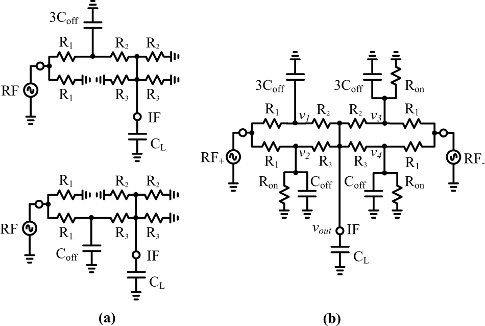
Figure 10. (a) Equivalent mixer quad assuming ideal  $R_{\mathrm{on}}$ when a branch with either R 2 (top) or R 3 (bottom) is conducting; (b) equivalent mixer quad assuming real $R_{\mathrm{on}}$ when a branch with R 2 is conducting.
Consequently, the solution of such a second-order differential equation can be written as:
 \begin{equation}
v_\mathrm{out}\left(t\right) = \rho \left(t\right) + c_{1}\cdot e^{-\beta_{1}t} + c_{2}\cdot e^{-\beta_{2}t}
\end{equation}
\begin{equation}
v_\mathrm{out}\left(t\right) = \rho \left(t\right) + c_{1}\cdot e^{-\beta_{1}t} + c_{2}\cdot e^{-\beta_{2}t}
\end{equation} with  $c_{\mathrm{1}}$, $c_{\mathrm{2}}$, $\beta_{\mathrm{1}}$, $\beta_{\mathrm{2}}$, and $\rho \left(t\right)$ given in Appendix A.
Using (18), the output IF voltage can be determined for each LO clock phase, where the initial conditions of the differential equation are determined from the preceding LO clock phase.
The above equation provides a much more accurate result for the phase responses of the two scaling branches for the third (and higher) harmonic. The only approximation left is the neglect of the on-resistance of the mixing switches. To address this, Figure 10(b) shows the signal path between the RF input and the IF output of the mixer quad during the first LO phase as an example, while including the on-resistance of the mixing switches. As can be seen, for a single scaling branch in a single LO clock phase, the off-capacitance of each of the four switches now plays a role. Furthermore, both differential RF inputs need to be considered. The resulting differential equation describing the output IF voltage as a function of time now becomes a fifth-order differential equation, which is too cumbersome to solve analytically. Instead, applying Kirchhoff’s current law (KCL) at both the intermediate mixing nodes (v 1, v 2, v 3, and v 4) as well as the IF output voltage node ( $v_\mathrm{out}$), we can write a system of five first-order differential equations (defined in Appendix B) that can be solved numerically. Similar to (18), the system is solved for a single LO clock phase where the initial conditions are determined from the preceding LO clock phase. This system was solved numerically using fourth-order Runge–Kutta (RK4) and provides the most accurate phase for the third and higher harmonics.
Design charts
Informed design decisions for the proposed mixer can be made based on the derivations in the previous subsections. It can be deduced from (3) that the input impedance is mostly dominated by the value of  $R_{\mathrm{1}}$. Thus, $R_{\mathrm{1}}$ should be chosen large enough to limit the RF input power. Secondly, the length of the switch should be chosen large enough such that the $C_{\mathrm{off}}$ dependence on its drain voltage is minimized. The width of the switch should be large enough such that $R_{\mathrm{on}}$ is much smaller than values of $R_{\mathrm{1}}$ and $R_{\mathrm{2}}$. Thirdly, with an initial switch size resulting in a certain $R_{\mathrm{on}}$ and $C_{\mathrm{off}}$, the values of $R_{\mathrm{2}}$ and $R_{\mathrm{3}}$ need to be chosen such that they satisfy both the IF bandwidth and HR requirements together. This selection can be eased by considering Figure 11, in which the IF bandwidth, HR, and conversion loss contours are plotted using the approximating resistive equations defined in (11). It visualizes that there is a trade-off between the IF bandwidth (requiring a small output impedance as defined in (7), i.e., small values of $R_{\mathrm{2}}$ and $R_{\mathrm{3}}$) and the conversion loss. Furthermore, in this resistive approximation, there are no phase errors, thus perfect HR is guaranteed as long as the magnitude scaling ratio between the two branches (see (9) and (10)) is equal to $1 + \sqrt{2}$, as illustrated by the solid black line in Figure 11 plotting the contour at which this ratio is equal to $1 + \sqrt{2}$.
Figure 11. Mixer design contours for IF bandwidth, third harmonic rejection ratio, and conversion loss vs. R 2 and R 3 for a chosen R 1 value.
While the approximate resistive equation defined in (11) is a good way to illustrate the HR concept, it is inaccurate since the phase errors of the two scaling paths were not included. As such, Figure 12 provides the design contours again, but now with the HR plotted by numerically solving the system of five first-order differential equations described in the previous subsection (and defined in Appendix B). We see that the trade-off between the IF bandwidth and the conversion loss still exists, but we also see that the HR ratio is no longer only dependent on the magnitude ratio between the two scaling paths but also starts to depend on the phase error introduced by these two scaling paths. The solid black line in Figure 12 gives the trajectory where the ratio between the down-converted component at the IF output node ( $IF_\mathrm{p}$ and $IF_\mathrm{n}$ as defined in Figure 2(c)) after mixing with the LO third harmonic from each of the two scaling paths equals one. In case of no phase error, the HR should thus peak along this trajectory where the ratio is equal to one. In Figure 12, we see that the HR does indeed peak along this trajectory; however, it peaks more for higher values of $R_{\mathrm{2}}$ and $R_{\mathrm{3}}$ indicating a lower phase error for these values.
Figure 12. Mixer design contours for IF bandwidth, third harmonic rejection ratio, and conversion loss vs. R 2 and R 3 for chosen R 1,  $R_{\mathrm{on}}$, and $C_{\mathrm{off}}$ values.
It should be noted that in all the equations derived, the values of  $C_{\mathrm{off}}$ and $R_{\mathrm{on}}$ were approximated as constant, determined as the average value inside each LO clock phase, where in reality they depend on the drain voltage, thus affecting the phase error of the scaling paths and the HR. Furthermore, any errors in phase or duty cycle of the LO clocks will also affect the HR. Consequently in a practical design, starting with the selected values of R 2 and R 3 from the design contours, simulations need to be run with the full switch model and the implemented clock generator. Any phase errors introduced in the clock generation circuitry can be beneficial if it cancels out the phase errors introduced by the two scaling paths, thus boosting HR. The final chosen values of R 1, R 2, and R 3 as shown in Figure 2(c) were fine-tuned by simulating the post-layout extracted mixer and clock generation chain combined.
Mixer implementation and measurements
The mixer, including the eight phase LO generation (Figure 2(d)), was implemented using thin-oxide transistors in TSMC 40 nm-CMOS technology. The mixer core occupies an area of 27 × 27 µm. Including the LO generation circuitry, the total mixer area is 133 × 57 µm (Figure 13(a)). All subsequent measurements are performed at a carrier frequency of 3.5 GHz targeting mMIMO base station applications. The mixer’s power consumption, including clock generation, is 40.7 mW from a 1.1 V supply.
Figure 13. (a) Fabricated chip micrograph of the voltage-mode mixer; (b) measurement setup and port impedances.
Conversion loss, linearity, and HR measurements were performed using the setup shown in Figure 13(b). The output losses due to cable connections and board traces were de-embedded. The measurement setup includes three single-tone signal generators where one source is used to generate the LO signal and the other two are used in combination with a power combiner to generate a two-tone RF input signal to the mixer. An off-chip balun is used after the power combiner to convert the generated single-ended two-tone signal into a differential one. The outputs are measured differentially with a high input impedance oscilloscope or single-ended with a source analyzer, the remaining outputs are terminated either with an open-circuit or 50 Ω impedances, respectively, depending on the instrument being used.
Since the final mixer application targets an on-chip IF ADC differential loading condition of 0.15 pF, the capacitive loading of the output pads (including the long output wires) was modified by adding more metal fillings to reach as closely as possible 0.3 pF. Consequently, the conversion loss must be measured with an instrument that has a high input impedance to not significantly load the mixer’s output. The conversion loss was, therefore, measured at a low IF frequency (1 MHz) using a Keysight oscilloscope (MSOS804A) with an input impedance of 1 MΩ $\parallel$14 pF connected at the I-mixer’s outputs, the outputs of the Q-mixer were connected to an open-circuit termination in this measurement as shown in Figure 13(b). This measurement yielded a conversion loss of 22.5 dB, which matches well with simulations in Figure 8, indicating the fabricated resistor ratios are accurate. Thus, confirming the targeted IF bandwidth of 800 MHz for the original intended differential capacitive loading of 0.15 pF, since the bandwidth (8) only depends on the same resistor ratios. The measured IF bandwidth is shown in Figure 15(a). The deviation from simulation is due to the non-perfect RF input balun’s response as well as input-output (IO) and electrostatic discharge (ESD) circuitry. The targeted IF output voltage swing of 0.2 Vpp for a maximum RF-input swing of 2.68 Vpp was also confirmed.
Using a source analyzer (R&S FSUP50) with 50 Ω IF port loading, the measured OIP3 proved to be 20 dBm across the mixer’s IF bandwidth (Figure 14(a)); a comparable performance was also achieved versus RF tone-spacing (Figure 14(b)). This is lower than the simulated linearity of the intrinsic mixer core (OIP3 > 24 dBm), this deviation could be explained by the impact of the IO-interconnect parasitics (bond wires and the nonlinearity due to the ESD protection circuits).
Figure 14. Linearity at fc = 3.5 GHz: (a) OIP3 vs. IF frequency with tone spacing = 20 MHz; (b) OIP3 vs. tone spacing with IF center frequency = 350 MHz.
The third harmonic rejection ratio (HRR3) was measured to be around 30 dB over the mixer’s IF bandwidth (Figure 15(b)). This somewhat reduced HRR3 was associated with an imbalance introduced by the on-chip balun connection. When including the balun imbalance and nonlinearity caused by the ESD protection within our simulations, they align well with the measurements.
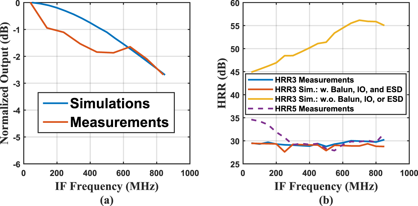
Figure 15. (a) IF bandwidth; (b) harmonic rejection ratio (HRR) at fc = 3.5 GHz.
Conclusions
A novel highly linear wideband harmonic-reject voltage-domain mixer topology is proposed and implemented in CMOS 40 nm. By circumventing the nonlinearity introduced by the variation of the mixer’s switches’ on-impedance and the need of power-hungry wideband linear-IF amplification, excellent linearity performance is achieved, making it an interesting candidate for the implementation of highly linear, wideband, low-power base station observation receiver applications. The realized mixer (despite its ESD and interconnect parasitics) offers excellent performance in terms of OIP3 (20 dBm) and IF bandwidth (800 MHz) while offering HR and quadrature down-conversion functionality, placing it favorably among previously reported state-of-the-art mixers when considering observation receiver applications, as can be concluded from Table 1.
Table 1. Performance comparison with wideband highly linear mixers
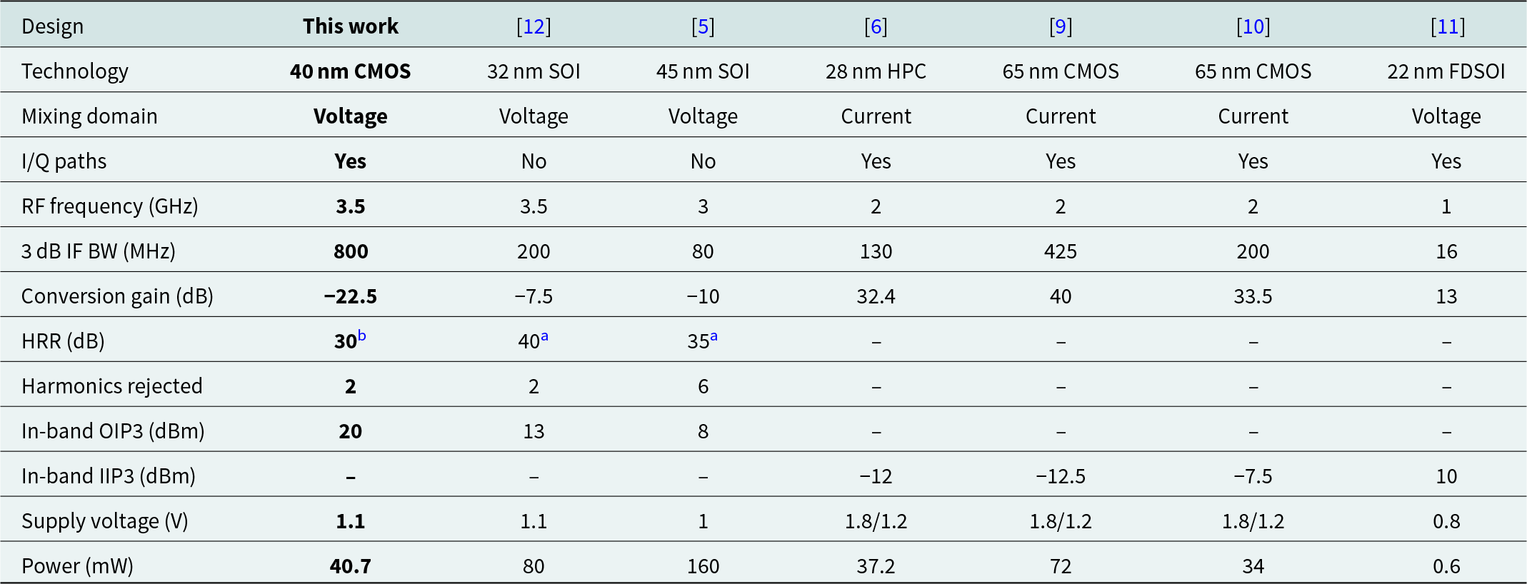
a Measured with GSSG probes.
b Measured with bond wires.
Acknowledgements
We would like to thank the Dutch Research Council (NWO), Ampleon Netherlands B. V., Nokia Bell Laboratories, and MediaTek for supporting this work. In addition, we would like to thank the people of Euro Practice (IMEC Leuven) for the provided IC design flow support.
Competing interests
The author(s) declare none.
Appendix A
Assume  $C_{\mathrm{2}}$ is the off-capacitance of the switch in a branch including $R_{\mathrm{2}}$, and $C_{\mathrm{3}}$ is the off-capacitance of the switch in a branch including $R_{\mathrm{3}}$. Thus, $C_{\mathrm{2}}$ and $C_{\mathrm{3}}$ can be written as:
 \begin{equation*}
\begin{aligned}
C_{2} &= 3\cdot C_{\mathrm{off}} \\
C_{3} &= C_{\mathrm{off}}.
\end{aligned}
\end{equation*}
\begin{equation*}
\begin{aligned}
C_{2} &= 3\cdot C_{\mathrm{off}} \\
C_{3} &= C_{\mathrm{off}}.
\end{aligned}
\end{equation*}The coefficients of the second-order differential equation (17) describing the mixer’s IF output voltage as a function of time when  $R_\mathrm{on}$ is neglected are presented below:
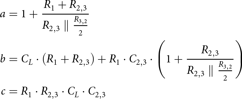 \begin{equation*}
\begin{aligned}
a &= 1 + \frac{R_{1} + R_{2,3}}{R_{2,3} \parallel \frac{R_{3,2}}{2}} \\
b &= C_{L} \cdot \left(R_{1}+R_{2,3}\right) + R_{1}\cdot C_{2,3}\cdot \left(1 + \frac{R_{2,3}}{R_{2,3} \parallel \frac{R_{3,2}}{2}} \right) \\
c &= R_{1}\cdot R_{2,3}\cdot C_{L}\cdot C_{2,3}
\end{aligned}
\end{equation*}
\begin{equation*}
\begin{aligned}
a &= 1 + \frac{R_{1} + R_{2,3}}{R_{2,3} \parallel \frac{R_{3,2}}{2}} \\
b &= C_{L} \cdot \left(R_{1}+R_{2,3}\right) + R_{1}\cdot C_{2,3}\cdot \left(1 + \frac{R_{2,3}}{R_{2,3} \parallel \frac{R_{3,2}}{2}} \right) \\
c &= R_{1}\cdot R_{2,3}\cdot C_{L}\cdot C_{2,3}
\end{aligned}
\end{equation*}where  $R_{2,3}$ and $C_{2,3}$ are equal to R 2 and C 2 when a branch with R 2 is conducting and are equal to R 3 and C 3 when a branch with R 3 is conducting. Similarly, $R_{3,2}$ and $C_{3,2}$ are equal to R 3 and C 3 when a branch with R 2 is conducting and are equal to R 2 and C 2 when a branch with R 3 is conducting.
The time-dependent term  $\rho\left(t\right)$ in the analytical solution (18) of this second-order differential equation is:
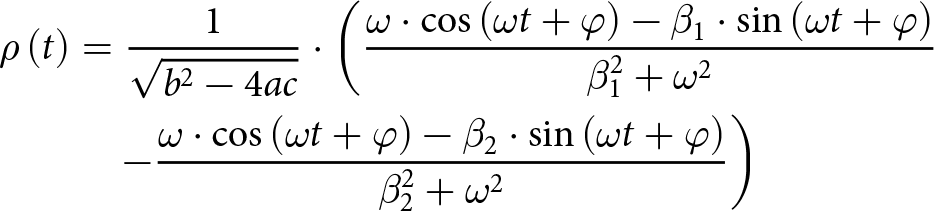 \begin{align*}
\rho \left( t \right) &= \frac{1}{\sqrt{b^2 - 4ac}} \cdot \left( \frac{\omega \cdot \cos{\left(\omega t + \varphi\right)} - \beta_{1}\cdot \sin{\left( \omega t + \varphi \right)}}{\beta_{1}^2 + \omega^2} \right. \nonumber\\
&\quad \left.- \frac{\omega \cdot \cos{\left(\omega t + \varphi\right)} - \beta_{2} \cdot \sin{\left( \omega t + \varphi \right)}}{\beta_{2}^2 + \omega^2} \right)
\end{align*}
\begin{align*}
\rho \left( t \right) &= \frac{1}{\sqrt{b^2 - 4ac}} \cdot \left( \frac{\omega \cdot \cos{\left(\omega t + \varphi\right)} - \beta_{1}\cdot \sin{\left( \omega t + \varphi \right)}}{\beta_{1}^2 + \omega^2} \right. \nonumber\\
&\quad \left.- \frac{\omega \cdot \cos{\left(\omega t + \varphi\right)} - \beta_{2} \cdot \sin{\left( \omega t + \varphi \right)}}{\beta_{2}^2 + \omega^2} \right)
\end{align*}where the coefficients β 1 and β 2 are defined as:
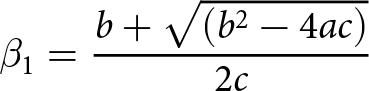 \begin{equation*}
\beta_{1} = \frac{b + \sqrt{\left(b^2-4ac\right)}}{2c}
\end{equation*}
\begin{equation*}
\beta_{1} = \frac{b + \sqrt{\left(b^2-4ac\right)}}{2c}
\end{equation*}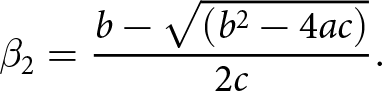 \begin{equation*}
\beta_{2} = \frac{b - \sqrt{\left(b^2-4ac\right)}}{2c}.
\end{equation*}
\begin{equation*}
\beta_{2} = \frac{b - \sqrt{\left(b^2-4ac\right)}}{2c}.
\end{equation*}Finally, the constants of the analytical solution (18) of this second-order differential equation are:
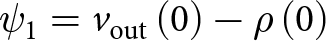 \begin{equation*}
\psi_{1} = v_\mathrm{out}\left(0\right) - \rho\left(0\right)
\end{equation*}
\begin{equation*}
\psi_{1} = v_\mathrm{out}\left(0\right) - \rho\left(0\right)
\end{equation*} \begin{equation*}
\psi_{2} = \rho'\left(0\right) - v_\mathrm{out}'\left(0\right)
\end{equation*}
\begin{equation*}
\psi_{2} = \rho'\left(0\right) - v_\mathrm{out}'\left(0\right)
\end{equation*} \begin{equation*}
c_{1} = \frac{\psi_{1}\cdot \beta_{2} - \psi_{2}}{\beta_{2} - \beta_{1}}
\end{equation*}
\begin{equation*}
c_{1} = \frac{\psi_{1}\cdot \beta_{2} - \psi_{2}}{\beta_{2} - \beta_{1}}
\end{equation*} \begin{equation*}
c_{2} = \frac{\psi_{1}\cdot \beta_{1} - \psi_{2}}{\beta_{1} - \beta_{2}}.
\end{equation*}
\begin{equation*}
c_{2} = \frac{\psi_{1}\cdot \beta_{1} - \psi_{2}}{\beta_{1} - \beta_{2}}.
\end{equation*}Appendix B
Assuming a differential single-tone sinusoid input with frequency ω and phase φ, by applying KCL at the four intermediate mixing nodes (v 1, v 2, v 3, and v 4) as well as the IF output voltage node ( $v_\mathrm{out}$) in Figure 10, one can arrive at the following system of five first-order differential equations:
 \begin{equation*}
v_\mathrm{out}'\left(t\right) = \frac{\frac{v_{1}\left(t\right)}{R_{2}} + \frac{v_{2}\left(t\right)}{R_{3}} + \frac{v_{3}\left(t\right)}{R_{2}} + \frac{v_{4}\left(t\right)}{R_{3}} - v_\mathrm{out}\left(t\right)\cdot\left(\frac{1}{R_{1}} + \frac{1}{R_{2}}\right)}{C_{L}}
\end{equation*}
\begin{equation*}
v_\mathrm{out}'\left(t\right) = \frac{\frac{v_{1}\left(t\right)}{R_{2}} + \frac{v_{2}\left(t\right)}{R_{3}} + \frac{v_{3}\left(t\right)}{R_{2}} + \frac{v_{4}\left(t\right)}{R_{3}} - v_\mathrm{out}\left(t\right)\cdot\left(\frac{1}{R_{1}} + \frac{1}{R_{2}}\right)}{C_{L}}
\end{equation*} \begin{equation*}
v_{1}'\left(t\right) = \frac{\frac{\sin{\left(\omega t + \phi\right)}}{R_{1}} + \frac{v_{out}\left( t\right)}{R_{2}} - v_{1}\left(t\right) \cdot \left( \frac{1}{R_{1}} + \frac{1}{R_{2}} \right) }{C_{2}}
\end{equation*}
\begin{equation*}
v_{1}'\left(t\right) = \frac{\frac{\sin{\left(\omega t + \phi\right)}}{R_{1}} + \frac{v_{out}\left( t\right)}{R_{2}} - v_{1}\left(t\right) \cdot \left( \frac{1}{R_{1}} + \frac{1}{R_{2}} \right) }{C_{2}}
\end{equation*}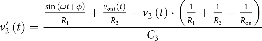 \begin{equation*}
v_{2}'\left(t\right) = \frac{\frac{\sin{\left(\omega t +\phi\right)}}{R_{1}} + \frac{v_{out}\left( t\right)}{R_{3}} - v_{2}\left(t\right) \cdot \left( \frac{1}{R_{1}} + \frac{1}{R_{3}} + \frac{1}{R_\mathrm{on}} \right) }{C_{3}}
\end{equation*}
\begin{equation*}
v_{2}'\left(t\right) = \frac{\frac{\sin{\left(\omega t +\phi\right)}}{R_{1}} + \frac{v_{out}\left( t\right)}{R_{3}} - v_{2}\left(t\right) \cdot \left( \frac{1}{R_{1}} + \frac{1}{R_{3}} + \frac{1}{R_\mathrm{on}} \right) }{C_{3}}
\end{equation*}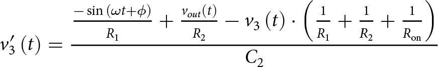 \begin{equation*}
v_{3}'\left(t\right) = \frac{\frac{-\sin{\left(\omega t + \phi\right)}}{R_{1}} + \frac{v_{out}\left( t\right)}{R_{2}} - v_{3}\left(t\right) \cdot \left( \frac{1}{R_{1}} + \frac{1}{R_{2}} + \frac{1}{R_\mathrm{on}} \right) }{C_{2}}
\end{equation*}
\begin{equation*}
v_{3}'\left(t\right) = \frac{\frac{-\sin{\left(\omega t + \phi\right)}}{R_{1}} + \frac{v_{out}\left( t\right)}{R_{2}} - v_{3}\left(t\right) \cdot \left( \frac{1}{R_{1}} + \frac{1}{R_{2}} + \frac{1}{R_\mathrm{on}} \right) }{C_{2}}
\end{equation*}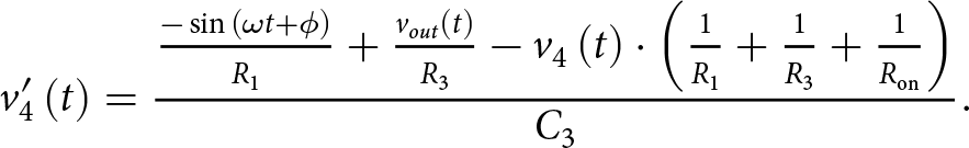 \begin{equation*}
v_{4}'\left(t\right) = \frac{\frac{-\sin{\left(\omega t + \phi\right)}}{R_{1}} + \frac{v_{out}\left( t\right)}{R_{3}} - v_{4}\left(t\right) \cdot \left( \frac{1}{R_{1}} + \frac{1}{R_{3}} + \frac{1}{R_\mathrm{on}} \right) }{C_{3}}.
\end{equation*}
\begin{equation*}
v_{4}'\left(t\right) = \frac{\frac{-\sin{\left(\omega t + \phi\right)}}{R_{1}} + \frac{v_{out}\left( t\right)}{R_{3}} - v_{4}\left(t\right) \cdot \left( \frac{1}{R_{1}} + \frac{1}{R_{3}} + \frac{1}{R_\mathrm{on}} \right) }{C_{3}}.
\end{equation*}This system of five first-order differential equations was defined for a mixer quad during one of the phases of the LO when RF+ is connected to an IF output through a conducting branch consisting of R 2, as shown in Figure 10. Similar equations can be written using KCL for the three remaining unique phases (namely, RF+ connected to the IF output through a branch consisting of R 3 and RF− connected to the IF output through a branch consisting of either R 2 or R 3). The IF output can thus be determined by numerically solving the respective system of differential equations in their respective LO clock phase, using initial conditions from the preceding LO clock phase.

Tariq Ibrahim received his M.Sc. degree (cum laude) from the Delft University of Technology, Delft, The Netherlands, in 2022, where he is currently pursuing his Ph.D. degree. His broad research interests span RF integrated circuits with a special focus on efficient linearization techniques for wideband digital transmitters (DTX).

Mohammadreza Beikmirza received his Ph.D. from the Delft University of Technology, Delft, The Netherlands, in 2023, where he continued his research as a postdoctoral fellow until 2024. He is currently with Nokia Bell Labs in Stuttgart, Germany.

Morteza S. Alavi is an associate professor at Delft University of Technology. His primary research interests include designing single-chip RF integrated circuits (RFICs) for wireless and cellular communication systems and CMOS wireline transceivers. He is a co-author of the book “Radio-Frequency Digital-to-Analog Converter,” published by Elsevier in 2016.]

Leo C. N. de Vreede received the Ph.D. degree (cum laude) from the Delft University of Technology, Delft, The Netherlands, in 1996. He is a Full Professor at the Delft University of Technology, where he is responsible for the Electronic Research Laboratory (ERL/ELCA). He has (co)authored more than 170 IEEE-refereed conference papers and journal articles. He holds several patents. His current interests include (digital-intensive) energy-efficient/wideband circuit/ system concepts for wireless applications. Dr. de Vreede was a (co)recipient of the IEEE Microwave Prize in 2008 and a Mentor of the Else Kooi Prize Awarded Ph.D. Work in 2010 and the Dow Energy Dissertation Prize Awarded Ph.D. Work in 2011. He was a recipient of the TUD Entrepreneurial Scientist Award in 2015.


 Open access