

Introduction
Millimeter-wave monolithic integrated circuits (MMIC) approach 1 terahertz (THz) operating frequencies [Reference Urteaga1, Reference Mei2], and there is a growing interest to use the 100 GHz–1 THz range for future communications and sensing solutions. In wireless communication, the data rate has been increasing exponentially over recent decades. A data rate of 100 Gbit/s has been forecast for 2020 [Reference Cherry3]. Ever more spectrum for wireless communication is needed, and it is readily available only at the sub-THz and THz range. For example, a 100 Gbit/s data link has been demonstrated at 237.5 GHz [Reference Koenig4].
THz imaging and sensing, for security and scientific (astronomy, earth science) applications utilize the THz regime above 300 GHz for radiometers and radars. The current commercial high-performance security radiometric systems use cryogenic bolometer arrays for sensors [Reference Luukanen and Pekola5], which provide low pixel price, but require complex and expensive cryogenic coolers, leading to high system overall price. MMIC-based radiometric or radar systems would enable room-temperature imagers, but they suffer from the lack of a cost-efficient integration method at THz frequencies.
The state-of-the-art method for MMIC integration is the split-block system, where a single component (e.g. LNA, detector) is housed within a brass block of roughly the size of (25 mm)3 [Reference Samoska6]. This leads to physically large systems. Further, the fabrication of such brass systems with demanded accuracy (3–5 µm) requires high-precision micromachining, with skyrocketing prices. This technology is not acceptable for mass production of THz systems. Wafer-level integration for sub-THz and THz systems has been suggested by several groups. These systems use micromachined waveguides on silicon to connect active MMICs together. A high-end process with six etch levels and its application to heterodyne arrays at 340 GHz with an external brass horn antenna is presented in [Reference Chattopadhyay7, Reference Jung-Kubiak8]. Further, a radiometric pixel with horn antennas included in silicon wafer-level packaging at 340 GHz is demonstrated in [Reference Radisic9].
Our vision for THz system integration (see Fig. 1) includes micromachined waveguides, but we aim to keep the process complexity at minimum to reduce the price of the integration, while still fostering the versatility of waveguide systems. For this goal, we use a low-cost microelectromechanical systems (MEMS)-micromachining process with only two etch depths and low temperature (below 160 °C or even room temperature) bonding processes allowing integration of MMIC.
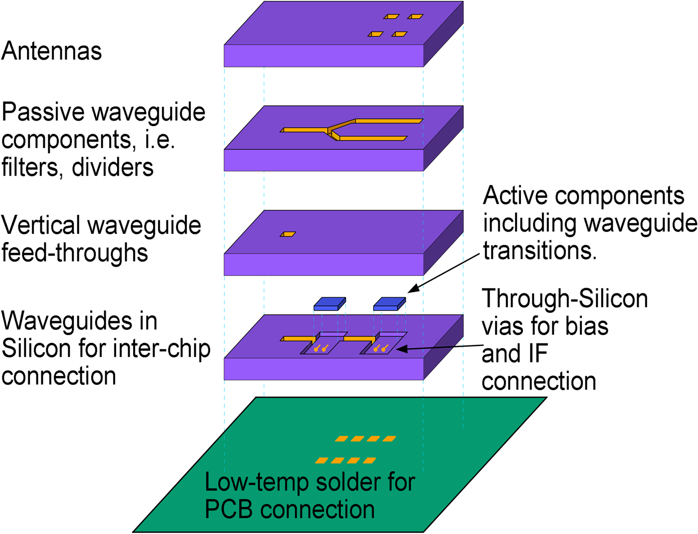
Fig. 1. Vision of 3D stackable wafer-level integration for THz system. Waveguides on silicon wafers connect active MMICs to each other for a compact system.
A key step in wafer-level integration processes is bonding, which is needed for stacking Si wafers. Low-temperature bonding process is required, because elevated temperatures causes mixing of Au and Si and raises surface roughness of metal in waveguides. Metal roughness is a critical parameter to obtain low losses in waveguides at the THz frequency range. Further, high bonding temperatures cannot be used after MMIC attachment, because it can melt the flip chip solder, and in extreme cases, the temperature can damage the active MMICs. Thus, new low-temperature bonding processes for wafer-level integration should be implemented in the process.
In this paper, we demonstrate key elements of a micromachining platform for integration of sub-THz and THz range subsystems, including waveguides, filters, and vertical vias, as well as transitions between the waveguide and the MMIC, all fabricated on the same wafers and process. Low-temperature Au/In and Au–Au laser bonding processes are utilized for stacking Si wafers in the integration platform. Successful implementation of such an integration platform would reduce the cost and size of high-performance multi-channel THz systems by orders of magnitude.
Design and fabrication methodology
The designed and fabricated components include straight WR-3 and WR-6 waveguides, WR-3 waveguides with bends, low-pass (LPF) and band-pass filters (BPF), through silicon waveguide vias and MMIC transition structure. The electromagnetic design of the structures has been carried out in Ansys HFSS version 15 and FEST3D 6.9.7 by Aurorasat.
Fabrication process
The fabrication process is based on deep reactive ion etching (DRIE) micromachining and wafer bonding technologies. The DRIE etch process is optimized for straightness of the waveguide walls and low roughness of gold layers. Three bonding technologies are evaluated for the platform: Au–Au and Au/In thermo-compression and Au–Au laser bonding.
Au–Au thermo-compression bonding
The waveguides are fabricated of two identical halves: half of the waveguide is processed in the lower silicon wafer, and the other half in the upper silicon wafer. Placing the waveguide with the E-plane along the wafer surface, the cut plane is in the middle of the H-plane side of the waveguide where there is no current component flowing through the cut-line. The waveguides are processed on silicon on insulator (SOI) wafers with 430 µm device layers. The SOI wafers are fabricated using direct bonding between double side polished (DSP) silicon wafers and thermally oxidized DSP wafers. The SOI wafers are manufactured at VTT, thinned down to correct thicknesses; chemical–mechanical planarization polished and finally thermally oxidized. Formed 862 µm thick SOI wafers are annealed at elevated temperatures. The 2 µm thick buried oxide layer is used as an etch stopper for DRIE etching. Processing includes two lithographically defined DRIE etch steps for two different structure depth heights (see Fig. 2(a)). The etch process steps are carefully optimized for straightness of the waveguide edges and level of each etch depth. After forming the waveguide structures, etched surfaces are thermally oxidized to remove polymer remnants and to smooth etched surfaces. This oxide is removed using HF wet etching. Processed wafers are finally gold plated with 1.6 µm thick sputtered Au layer, which results in a sidewall thickness of at least 0.6 µm.
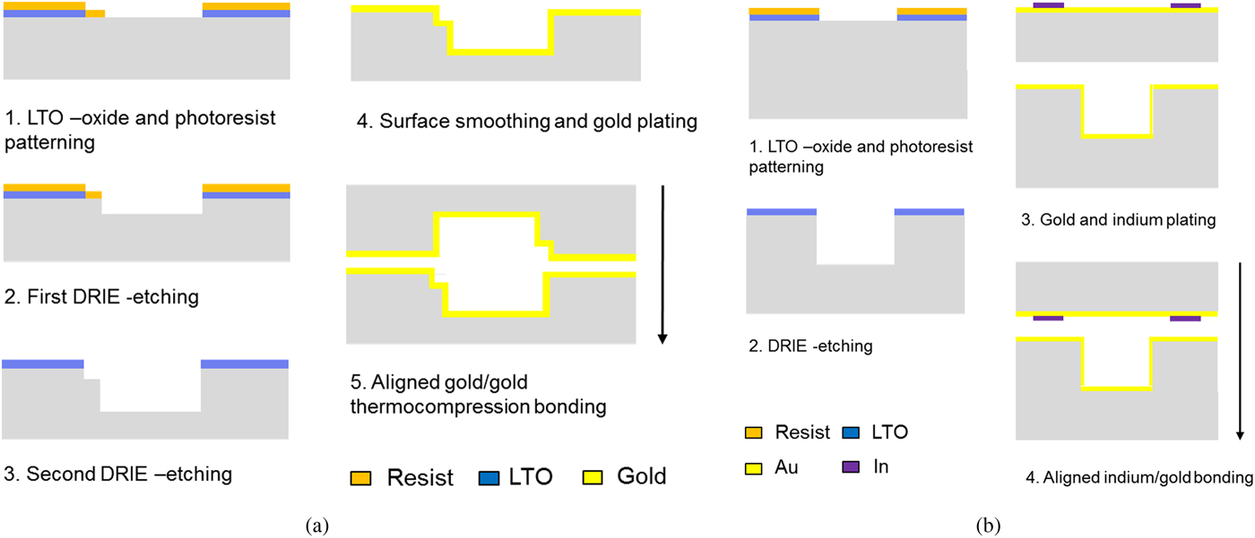
Fig. 2. (a) Simplified process flow using Au/Au thermo-compression bonding, (b) process flow for low-temperature Au/In bonding.
The gold-plated SOI wafer pairs containing half waveguide structures are bonded together using wafer-level optically aligned Au–Au thermo-compression bonding. The thermo-compression bonding is accomplished with bonding temperatures between 300–450 °C. Gold thermo-compression bonding is attractive because it provides a highly conductive bond between the wafers. Also, gold does not readily form an oxide like Cu–Cu or Al–Al thermo-compression bonding. Thus, under the standard Au–Au wafer bonding conditions, it is not necessary to use excess surface cleaning prior to bonding. The pair of aligned waveguide wafers were inserted into an EVG510 wafer bonder and subjected to 400 °C temperature for 30 min and bonding pressure applied to the wafer pairs of 40 kN. The use of a 1.6 µm thick gold layer, moderate temperatures, and pressures results in uniform, strong, and electrically conductive bond between the waveguide wafers. The bonded wafer pairs cannot be separated without using excessive force and breaking the underlying silicon substrate. Finally the 1724 µm thick wafers are cut into chips using narrow pre-etched cutting grooves on the dicing streets and combined with mechanical dicing from both wafer sides. Examples of fabricated structures are shown in Fig. 3.
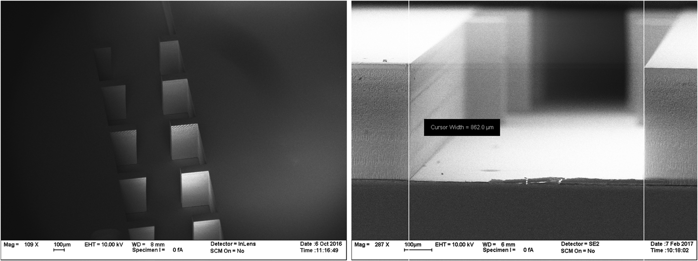
Fig. 3. SEM images of a band-pass filter.
Through-wafer waveguide vias to connect several layers of the components are also fabricated. These vias are realized as H-plane corner bends, as seen in the cross-section in Fig. 13. These vias are defined on the handle side of the SOI wafers using two-sided aligned contact lithography. The vias are then etched through the handle silicon layer using a single etch step.
With the same process we also demonstrated WR-6 waveguides and WR-3 BPFs in horizontal position between the wafers.
Low-temperature Au/In bonding
The waveguides are designed to be fabricated in two distinct silicon wafers. The waveguide structure is processed in the lower silicon wafer, and then capped with a flat upper silicon wafer (see Fig. 2(b)). We fabricated WR-3 waveguides and WR-3 BPFs on the lower wafers with the E-plane along the wafer surface. The waveguides were formed using a single depth DRIE etch step. The waveguides are processed on 882 µm thick SOI wafers with 430 µm thick structure layers and 450 µm handle layers. The SOI wafers containing the waveguide structures are capped with flat 400 µm thick DSP wafers. Two shallow etch steps are needed for wafer- and chip-level alignment marks and one deep DRIE etch for the waveguide formation. The DRIE etch process step is optimized for straightness of the waveguide edges. The 400 µm thick cap wafers are thermally oxidized and patterned. The SOI wafers and the DSP cap wafers are finally gold-plated.
The thin 1 µm indium layer used for low-temperature Au-In bonding between the cap and the SOI wafer is electrochemically deposited and patterned lithographically over the gold layer on the cap wafers (see Fig. 2(b)). The cap wafer is bonded to the SOI wafer using low-temperature Au–In bonding on wafer level. A eutectic alloy of Au–In is a two-component alloy that undergoes a direct solid-to-liquid phase transition at a specific composition and 157 °C eutectic temperature. The wafer pairs are heated over the eutectic temperature during the bonding process until the Au–In interface mixes to form a eutectic alloy via diffusion. Indium has excellent adhesive properties to most metals, also to gold. Adhesion at the Au–In interface is generally known to be as great as the bulk strength of indium. The aligned cap wafer is bonded on the SOI wafer using optically aligned bonding in an EVG510 wafer bonder subjected to 160 °C temperature for 10 min and applied bonding pressure of 20 kN to the wafer pairs. The process temperature is considerably lower than the temperature used in the Au–Au thermo-compression.
Chip-level laser bonding
In case of chip-level laser bonding, the gold-plated cap wafers manufactured for the laser bonding are fabricated without the In layer (see Fig. 2(b)). Au–Au bonding is demonstrated at room temperature utilizing a pulsed near-infrared (NIR) laser. The laser bonding was demonstrated after dicing, on chips with the dimensions of 10 × 10 mm. A Xiton Photonics IDOL-1.34-Q laser operating at 1342 nm, a pulse width of 5 ns, and a repetition rate of 50 kHz is used for bonding. The laser beam is focused onto a 50 nm titanium tungsten (TiW) adhesion layer below the 550 nm gold layer through the 400 µm silicon wafer. High resistivity silicon (>10 kΩcm) for the cap wafer is necessary to allow optical transmission in the NIR range. To increase laser coupling to the TiW, a silicon nitride (SiN) antireflective layer is deposited between the silicon and TiW layers. Each laser pulse acts independently to cause highly localized short-term heating of the compressed Au–Au interface to achieve bonding. Areas larger than the laser spot size are bonded by scanning the laser spot horizontally.
The laser beam is expanded at its output to a spot diameter of 3 mm. The laser beam is split for monitoring purposes with a broadband 50/50 beam splitter. Half of the beam is focused normal to the cap wafer surface through a 75 mm focal length achromatic objective. Focus is adjusted to minimize the spot size at the TiW layer.
The laser bonding process limits the maximum thickness of gold on the wafer where the laser is focused. In the case of an ideally focused beam, the volume that must be heated to bonding temperature increases in proportion to the cube of the layer thickness if this volume is approximated to be a sphere around the laser spot. This volume must intersect with the Au–Au interface plane for bonding to occur. Thicker gold layers require significantly higher pulse energy. A pulse exceeding the energy density limit of the SiN–TiW interface causes destructive ablation. At a given pulse energy, lowering the energy density at the SiN–TiW interface can only be achieved by increasing laser spot size. However, this increases the volume that must be heated to bonding temperature in the plane of the layers. It also decreases the bonding resolution for small devices. We have found a layer thickness of approximately 500 nm to function well with our optical system achieving a bonding linewidth of approximately 20 µm.
To check the quality of laser bonding, a bonded module was sheared and inspected. Images of surfaces of two halves of the module are shown in Fig. 4. In (a), dark regions are heated Au, and light regions are exposed SiN. In (b), dark regions are TiW transferred from the cap wafer, and light regions are smooth Au. The regions where Au and TiW have been delaminated from SiN on image (a) correspond to the regions of excess TiW on (b). Delamination at the SiN–TiW interface shows that the Au–Au bond strength exceeds that of SiN–TiW. Ultimate bond strength is limited by the quality of SiN–TiW bonding rather than by the quality of laser bonding.
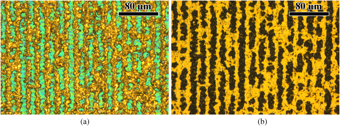
Fig. 4. Microscope images of cap (a) and bottom (b) Si halves after laser bonding. One image has been mirrored horizontally to illustrate pattern correspondence.
Measurement setup
The S-parameters of the fabricated waveguide dies were measured with an Agilent PNA-X vector signal analyzer with V03VNA2 millimeter-wave extenders from Oleson Microwave Labs for H-band. Different brass sample holders were fabricated for connecting the silicon samples to the waveguide interface of the measurement setup. The sample holder with side entry is realized as a split-block structure, where the silicon die is pinched between the two halves of the brass holder structure. The dies with the side entry are equal in size and the same holder can be utilized just by changing the silicon sample. One of the realized structures has waveguide openings on top and bottom of the silicon die and different brass holder structure was needed. In this case, the silicon die is placed on a frame and sandwiched between two thicker brass sheets with waveguide openings. Thru-reflect-line calibration was performed at the waveguide interface [Reference Engen and Hoer10]. The brass holders with silicon dies and its connection to the measurement system are shown in Fig. 5.
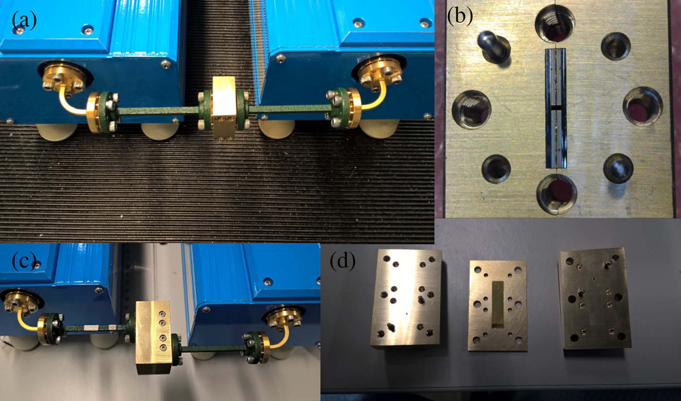
Fig. 5. Measurement setups for the fabricated silicon dies: (a) and (b) sample holder for dies with side entry; (c) and (d) sample holder for dies with top and bottom entry.
Results
Waveguides
The WR-3 (Fig. 6) waveguide has standard cross-sections of 0.43 mm × 0.86 mm and lengths of 10 mm. The waveguide was fabricated with Au/Au thermo-compression bonding. The frequency band of WR-3 is 220–325 GHz. The waveguide was fabricated with one etch depth of 430 µm. The WR-3 was placed vertically between the wafers as shown in Fig. 6. The measured (simulated) insertion loss for a 10 mm waveguide is 2.3 dB (0.2 dB) at 270 GHz.
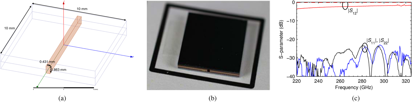
Fig. 6. Silicon micromachined WR-3 waveguide: (a) simulation model, (b) photograph of the bonded die, (c) simulated (dashed line) and measured (solid line) S-parameters.
The WR-3 waveguides with bends (Fig. 7) include straight waveguides and four bend waveguides with a bend radius of 1 mm resulting in a total length of 14.2 mm. A designed E-plane bend is fabricated with Au/Au thermo-compression bonding. The measured (simulated) insertion losses for a 10 mm die at 270 GHz were 3.4 dB (0.2 dB) for a curved bend. The waveguide length is 14.2 mm, which equals to a similar attenuation per length as in a straight waveguide.
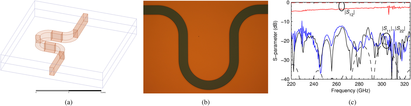
Fig. 7. WR-3 waveguide with bends: (a) simulation model, (b) micrograph of a manufactured structure, (c) simulated (dashed line) and measured (solid line) S-parameters.
A WR-6 waveguide was also designed and fabricated in the Au/Au thermo-compression bonding process (see Fig. 8). The waveguide has standard cross-sections of 0.83 mm × 1.65 mm and lengths of 10 mm. The waveguide was placed horizontally between the wafers, and it measures 862 × 1651 µm. The measured (simulated) insertion loss for a 10 mm waveguide is 1.0 dB (0.06 dB) at 140 GHz.
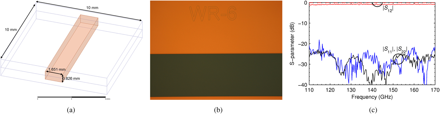
Fig. 8. Silicon micromachined WR-6 waveguide: (a) simulation model, (b) micrograph of a manufactured structure, (c) simulated (dashed line) and measured (solid line) S-parameters.
To test the applicability of low-temperature bonding processes for the integration platform, WR-3 waveguides are fabricated with Au/Au and Au/In thermo-compression bonding and Au–Au laser bonding. Fabricated waveguides are tested and results for a 10 mm long waveguide are given in Fig. 9.
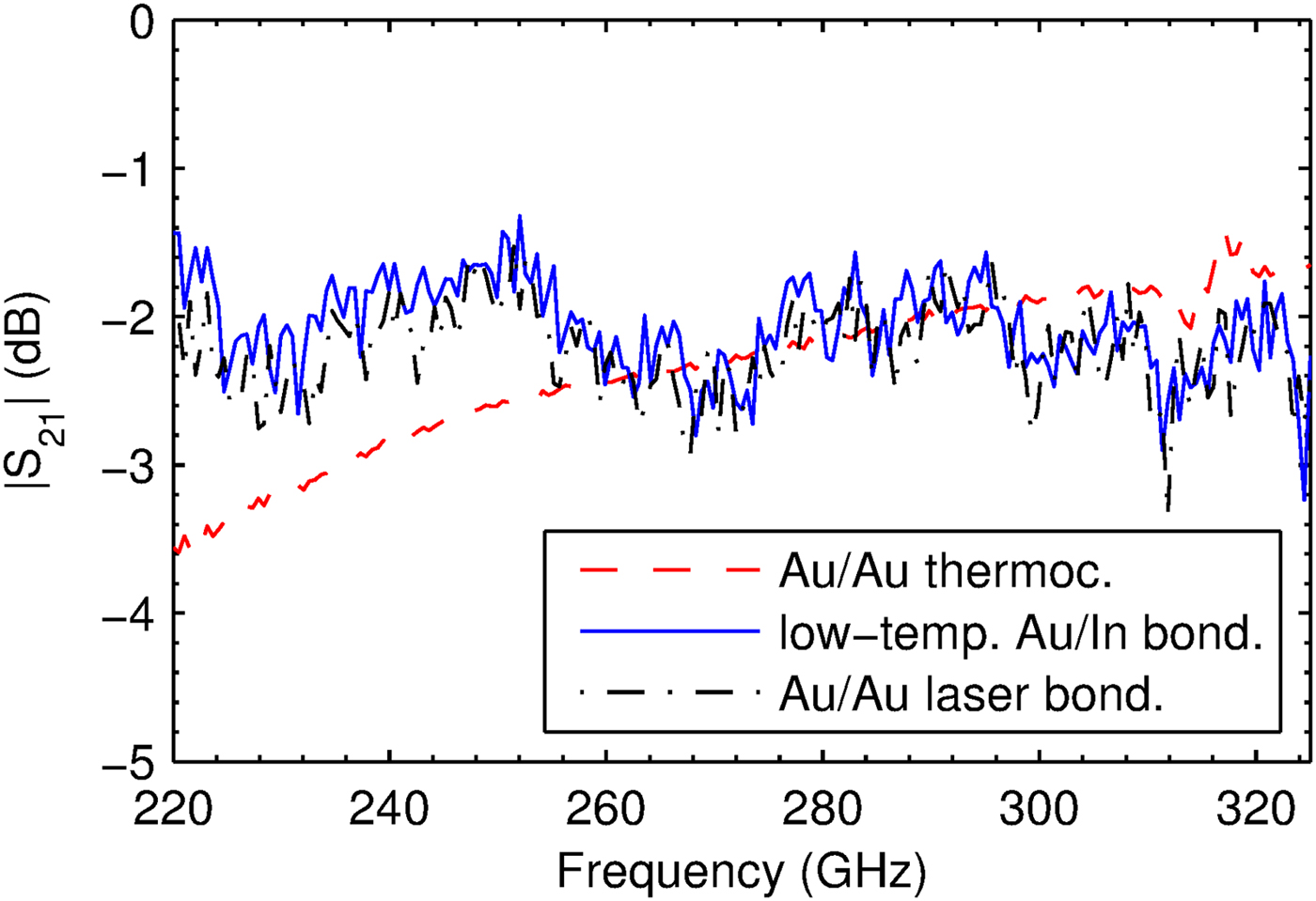
Fig. 9. Measured transmission coefficients of silicon micromachined WR-3 waveguides manufactured using Au/Au and Au/In thermo-compression bonding and laser bonding.
It can be seen that waveguides fabricated using low-temperature bonding technologies have performance similar with waveguides fabricated with Au/Au thermo-compression. Components fabricated with Au/Au thermo-compression bonding demonstrate higher losses in the frequency range 220–265 GHz. This effect will be discussed in section ‘Discussion’. Some ripples can be observed for samples fabricated with the usage of Au/In thermo-compression bonding and laser bonding. A possible reason is a 100 µm mismatch for these samples of their thicknesses and the area for them in the chip holder. Two sources for the ripple are possible. The first one is the misalignment of the Si waveguide and waveguide in the interface of the measurement setup. In addition, the silicon did not fill the fixture gap completely, so there could be a signal leakage through the air.
Filters
The filter designs are based on classical waveguide filter topologies similar to the ones shown in [Reference Leal-Sevillano11, Reference Leong12]. The filters were synthesized using FEST3D. The (Fig. 10) is designed for a highest transmission frequency of 280 GHz with return loss >20 dB. The LPF is realized with periodic and symmetric capacitive irises in the E-plane. The used iris thickness is 100 µm. The BPF (Fig. 11) has symmetric inductive irises in the H-plane. The passband is defined between 260 and 280 GHz with return loss >20 dB, which results in a filter order N = 5, i.e. five resonator cavities. Demonstrated filters are fabricated with Au/Au and Au/In thermo-compression bonding and Au–Au laser bonding. To achieve the structures in the same process run, the BPF is fabricated horizontally; etching only one of the wafers with the waveguide structure and capping it with a unetched wafer (see Fig. 11). The measured (simulated) insertion loss for the LPF at 270 GHz is 3.3 dB (0.3 dB), whereas the return losses are >15 dB (>20 dB). For the BPF, the insertion loss is 5.6 dB (0.5 dB) and the return loss is >13 dB (>20 dB) at 270 GHz.
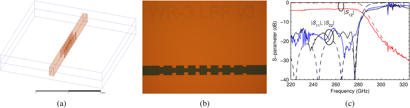
Fig. 10. WR-3 low-pass filter fabricated with Au/Au thermo-compression bonding: (a) simulation model, (b) micrograph of a manufactured structure, (c) simulated (dashed line) and measured (solid line) S-parameters.
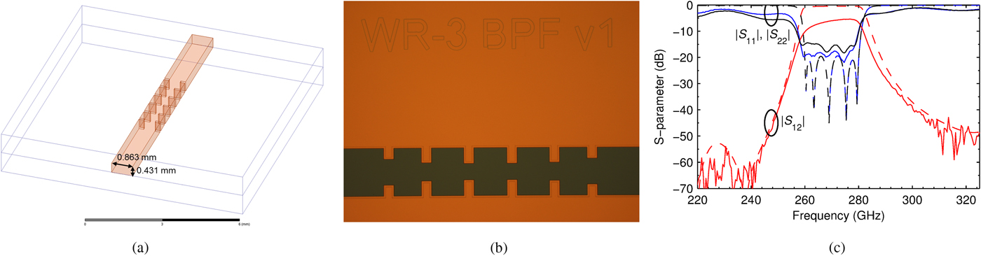
Fig. 11. WR-3 band-pass filter fabricated with Au/Au thermo-compression bonding: (a) simulation model, (b) micrograph of a manufactured structure, (c) simulated (dashed line) and measured (solid line) S-parameters.
Fig. 12 shows the characteristics of WR-3 BPF fabricated with Au/In thermo-compression bonding. The insertion loss is 2.6 dB (0.8 dB) and the return loss is >15 dB (>16 dB) at 290 GHz. The insertion loss is about 3 dB lower than for WR-3 BPF fabricated with Au/Au thermo-compression bonding shown in Fig. 11.
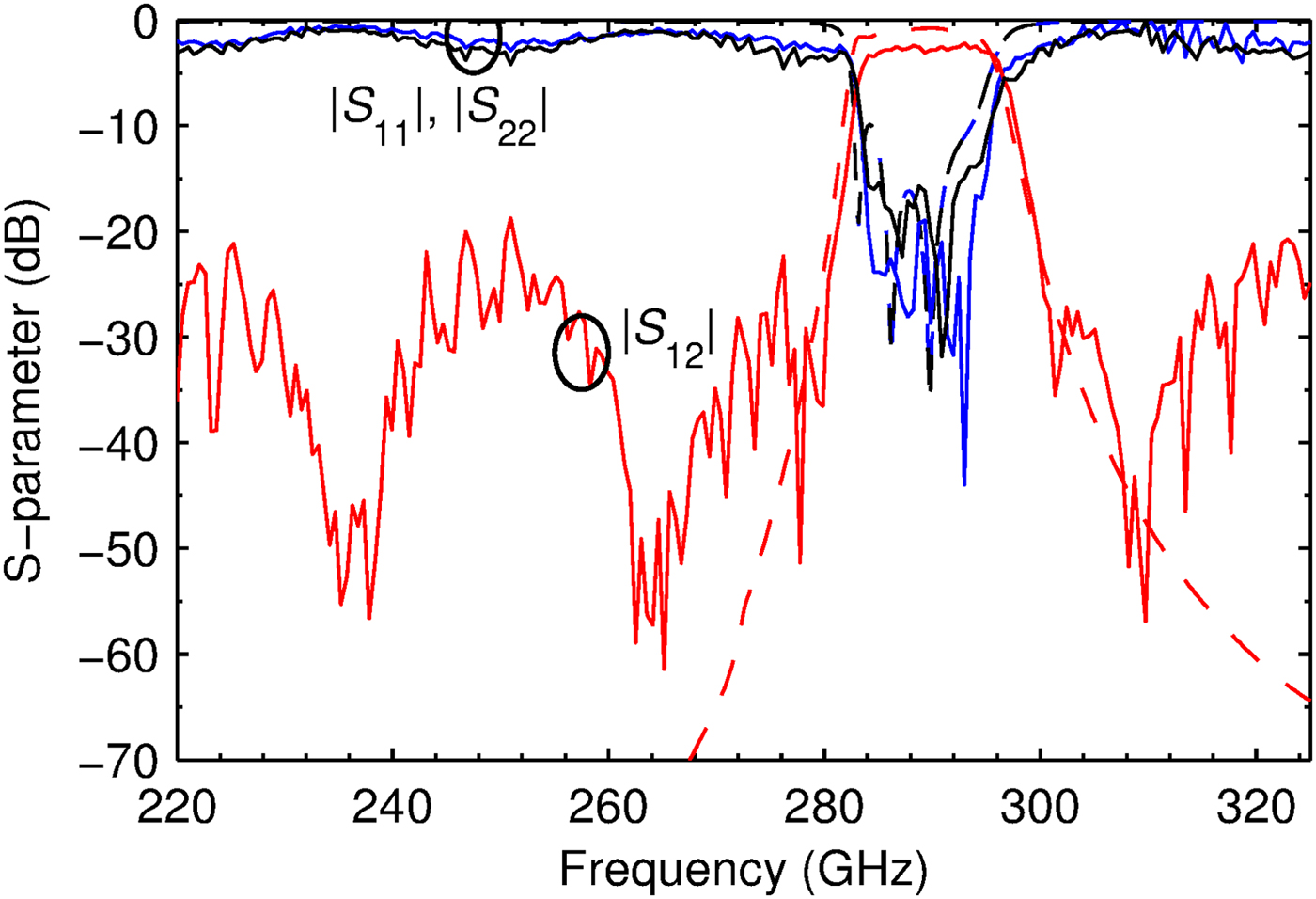
Fig. 12. WR-3 band-pass filter fabricated with Au/In thermo-compression bonding: simulated (dashed line) and measured (solid line) S-parameters.
As in the case of waveguides, we can see that components fabricated using different bonding technologies have similar performance. We can see a good match of measured and simulated results of structures with fabricated geometries. Filters fabricated with Au/Au thermo-compression demonstrate higher losses in the frequency range 220–265 GHz. This effect will be discussed in section ‘Discussion’.
Vias
For system integration presented in Fig. 1, key components include through-wafer vias to connect several layers of components. The through silicon waveguide vias are realized as H-plane corners, as seen in the cross-section in Fig. 13. The corners are mitered with a 300 µm × 300 µm cut-off for optimum impedance matching. The via structures are fabricated with Au/Au thermo-compression bonding process. The measured (simulated) insertion losses for a 15.7 mm long via are 2.6 dB (0.3 dB) at 270 GHz (Fig. 13). Due to the sample holder assembly, the measured losses also include the losses of the brass waveguides of the holder (see Fig. 5).
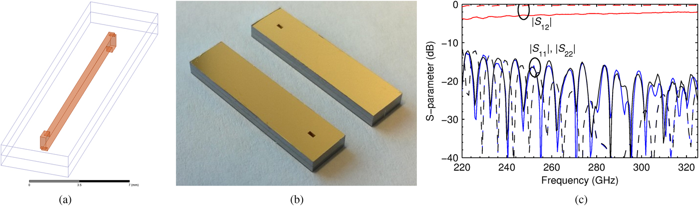
Fig. 13. WR-3 through-wafer via: (a) simulation model, (b) photograph of two manufactured structures, (c) simulated (dashed line) and measured (solid line) S-parameters.
MMIC connection
A critical feature is the ability to integrate MMICs to waveguides (Fig. 14). This is demonstrated by designing an MMIC with a microstrip line having radiative probes at both ends in a similar way like those presented in [Reference Samoska6]. The probes are designed to couple between the microstrip line and WR-3 waveguides as shown in Fig. 14. The probe is a radial stub with a length of 0.14 mm and an opening angle of 45°. The probe is aligned at the center in the E-plane, i.e. at the maximum electric field in the WR-3 waveguide, 0.26 mm (~λ 0/4) apart from the WR-3 end. The microstrip line is placed inside a channel with metallized walls. The channel width of 0.2 mm is used to prevent waveguide modes inside the channel. In addition, the microstrip line substrate thickness of only 50 µm is chosen to avoid quarter-wavelength resonances inside the substrate. It was observed in simulations that coupling between the probe and a waveguide is sensitive to the longitudinal position of the probe inside the waveguide. For example, with 50 µm misalignment, the insertion loss is increased from 0.7 to 2 dB. For accurate microstrip probe MMIC alignment, mechanical width steps were designed both in the MMIC chip and in the MMIC channel. A fabrication tolerance of 30 µm was left for the alignment structures. The microstrip line is fabricated in a separate process to High-Res silicon, which have been thinned down to 50 µm. The microstrip line with waveguide transition structures was placed between the waveguide halves prior to bonding. The measured (simulated) insertion losses for the WR-3-to-microstrip back-to-back transition at 270 GHz are 4.4 dB (1.3 dB).
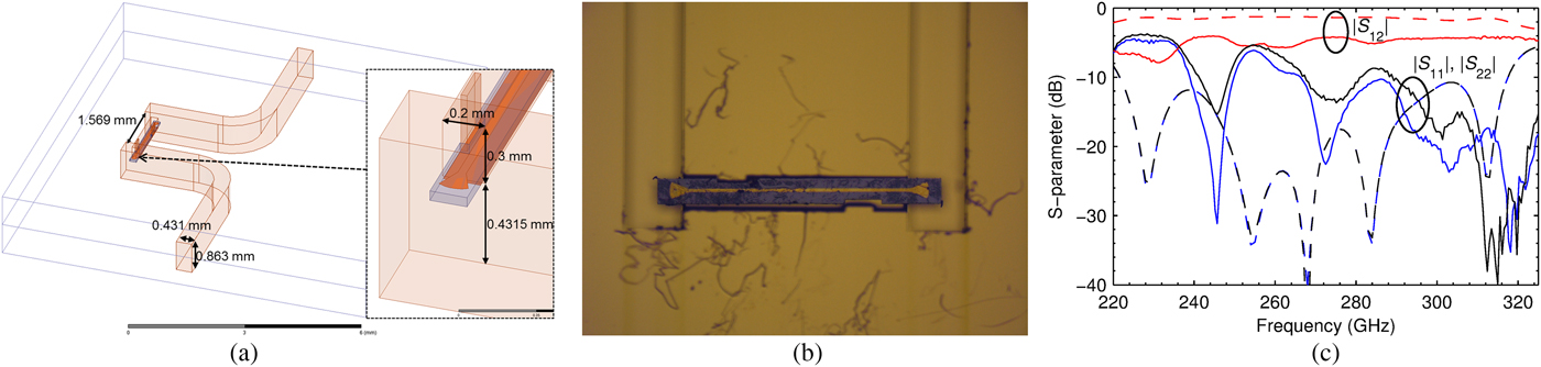
Fig. 14. WR-3-to-microstrip probe transition: (a) simulation model, (b) micrograph of a manufactured structure, (c) simulated (dashed line) and measured (solid line) S-parameters.
Discussion
Measurements of all fabricated structures exhibit expected frequency performance but higher loss than the simulations and particularly higher losses for lower frequencies.
The gold thickness has been measured to be 0.6 µm in the waveguide walls, which is well above the skin depth of 0.14 µm at 300 GHz. However, it was found that for components from the first manufacturing lot that the final oxidation step did not successfully fill the 2 µm gap in the metallization at the waveguide corner due to vapor hydrogen fluoride (VHF) over etching of silicon dioxide. It has been detected as a source of extra losses, especially for the lower frequency range in similar structures before, e.g. in [Reference Leal-Sevillano11], where a 7 µm gold layer is used to fully cover the waveguide corners. Figure 15(a) shows a SEM image of the WR-3 waveguide bottom corner, showing small gaps in the corners due to notching effect in the DRIE process, i.e. an undercut as seen in [Reference Kirby13].
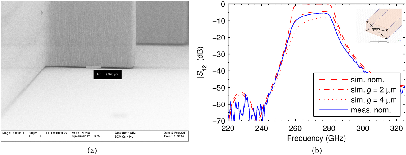
Fig. 15. SEM image showing the 2 µm gap in the metallization at the waveguide corner due to over etching. (b) Effect of small longitudinal gaps of width g in the WR-3 corners on the transmission coefficient.
Figure 15(b) shows simulations with a 2 or 4 µm gap in gold in the corners of the waveguide for the BPF. The simulated results with a 2 µm gap comply very well with the measured results.
The problem of the gap was fixed for the fabrication lot with Au/In thermo-compression and Au–Au laser bonding. The fixing was done by shortening the VHF etching time and adding a polysilicon deposition step followed by a dry oxidation of the waveguide walls in the manufacturing process. It can be seen in Figs 9 and 12 that losses of such components are no more high at low frequencies than observed for the components fabricated in the first lot. However, the level of losses is not improved considerably. The components have higher than simulated losses. The possible reason for the high loss is quality, particularly the roughness of metal in waveguides and/or losses at the interface of silicon chips and measurements flanges.
Conclusion
We demonstrate a wafer-level integration method based on micromachined waveguides on silicon. The key components are demonstrated, including waveguides, low frequency and BPFs, vias, and MMIC-waveguide transition at the frequency range 225–325 GHz. The developed process uses two DRIE etch depths for cost-efficiency. Low-temperature bonding, namely Au/In thermo-compression bonding, and laser bonding options integrated in the process allow easy integration of MMIC. The connection between the silicon die and brass waveguides requires complicated mechanics with high precision, and is expensive and leads to cumbersome systems. Thus, the final goal of the integrated systems should be a system where all the millimeter-wave components, including the antenna, are within the silicon die. The remaining intermediate frequency (IF) and bias interfaces can be handled with standard pads and solder processes.
 Vladimir Ermolov graduated with honors in 1981 and received the Ph.D. in 1986 from the Moscow Engineering Physics University (MEPhI). Since 1981, he has been a Senior Research Associate with the Laboratory of Dielectric Devices (MEPhI). He worked many times as a Visiting Researcher in the Department of Physics, Helsinki University and Fraunhofer Institute of Non-destructive testing, Germany. He has been a Principal Research Scientist with the Nokia research center from 1998 to 2011, where he worked as a Project Manager for many projects in the areas of MEMS, nanotechnology, radiotechnology, mass memory technology, and sensors. He was involved in the commercialization of several technologies. Since 2011, he has been with the VTT Technical Research Center of Finland as a Principal Research Scientist, where he has made project management and research in the areas of radiotechnology, MEMS, nanotechnology, and technology commercialization. He is the author and co-author of 54 referred journals and the holder and co-holder of 47 patents and patents pending.
 Antti Lamminen received the M.Sc. (Tech.) degree in Electrical Engineering from Aalto University, Espoo, Finland, in 2006. He has been a Research Trainee with the Antennas and RF Technologies Team, VTT Technical Research Centre of Finland, Espoo, Finland, since 2005, where he has also been a Research Scientist since 2006. His current research interests include beam-steerable millimeter-wave antennas and arrays, filters, and other passive components from microwave up to terahertz frequencies.
 Jaakko Saarilahti received his Ph.D. in Applied Physics from Helsinki University of Technology in 1995. He is working as a Senior Scientist at VTT in Microsystems and Nanoelectronics. His focus has been on thin film and silicon process technologies and MEMS. Dr. Saarilahti is a specialist in silicon surface micromachining technology. His current research activities are in design and process development of MEMS devices such as pressure sensors, ultrasonic transducers, gas detectors, microphones, magnetometers, and waveguides. Dr. Saarilahti has authored and co-authored over 60 international publications.
 Ben Wälchli is a M.Sc. Student at the Department of Physics, University of Helsinki and has been involved with the research and development of experimental optical systems since 2010. He has been a Research Trainee at VTT Technical Research Center of Finland since 2013 developing measurement methods for optical devices, including MOEMS and silicon photonic components. His current work involves development of methods for integration of microfabricated devices and silicon photonic components.
 Mikko Kantanen received the M.Sc., Lic.Sc., and D.Sc. degrees in Electrical Engineering from Aalto University (formerly Helsinki University of Technology), Espoo, Finland 2001, 2006, and 2017, respectively. Since 2001, he has worked in MilliLab, VTT Technical Research Centre of Finland Ltd., Espoo, Finland, currently as a Senior Scientist. His research interests include millimeter-wave integrated circuit design, millimeter-wave measurements, and millimeter-wave systems. Mr. Kantanen is a recipient of the 47th European Microwave Conference Microwave Prize and a co-recipient of the Asia-Pacific Microwave Conference 2006 Prize.
 Pekka Pursula received the M.Sc. degree (with distinction) and D.Sc. in Technical Physics from Aalto University (formerly Helsinki University of Technology), Helsinki, Finland, in 2002 and 2009, respectively. During 2002, he was with the Philips Medical Systems Finland developing the RF systems in magnetic resonance imaging (MRI). Since 2003, he has been with the VTT Technical Research Centre of Finland, where he is currently the Research Team Leader. His research interests include wireless sensor systems from UHF and millimeter-wave frequencies and radars. From 2011, he is also an Adjunct Professor of Electronics at Tampere University of Technology. In 2012, Dr. Pursula was a Visiting Researcher at IMTEK Department of Microsystems Engineering at the University of Freiburg, Germany. D.Sc. Pursula is the Vice Chair of IEEE MTT/AP/ED chapter in Finland since 2014. He received the Young Scientist Award at the URSI/IEEE XXIX Finnish Convention on Radio Science, Espoo, Finland, November 1–2, 2004. He has authored and co-authored over 40 peer-reviewed journal and conference articles, and he is a co-inventor of eight patent applications.


