

I. INTRODUCTION
Microwave photonics has been an area of research since last decade as it offers several advantages such as wider bandwidth, low loss, high data rate, low weight, immunity against electromagnetic interferences (EMIs), etc. [Reference Seed1, Reference Seed2]. Although this technology is used in cable network and sensors remoting, its application in radar is still being explored [Reference Capmany and Novak3, Reference Pappert and Krantz4]. Microwave photonics in radar has many applications starting from radio frequency (RF) front end, moving target indication filters to radar signal processing [Reference Pan, Zue and Zhang5]. However, distribution of RF, and digital signals in active electronically scanned array (AESA) radars using microwave photonic network has not been proposed yet.
Photonic application is also found in analog beam-forming network of phased array radars. True time-delay circuits were formed with the help of fiber Bragg grating to synthesize multiple squint-free beams with high instantaneous bandwidth over a wide range of microwave frequencies [Reference Minasian and Alameh6]. An extension of this technology for variable time delay with carrier reference circuit eliminates the need of frequency conversion [Reference Berceli, Herczfeld, Daryoush and Rosen7]. In contrast AESA radar uses digital beam forming network in which digital word is preloaded thus eliminating the need of multiple interconnect functions.
AESA radars are multifunction multibeam radars which scan in azimuth and elevation electronically and thus performs tracking, surveillance, and other functions. The principle of coherent pulse Doppler AESA radar is to preserve the phase of transmitted pulse and compare it with that of receive echo to arrive at target information [Reference Skolnik8]. The requirement of narrow receive pencil beam increases antenna aperture dimensions, leading to a sizeable number of transmit/receive (T/R) modules physically spread across the antenna aperture. Each T/R module requires a number of RF and data cables. The layout of antenna array in an AESA radar is a challenge in comparison to conventional reflector based radar antenna.
Conventional scheme for distribution of RF and digital signals are through coaxial and multicore cables. They are inherently lossy and mechanically complex considering weight and volume constraints of multichannel rotary joint. In contrast, optical systems are immune to EMI and electromagnetic compatibility (EMC) issues while providing large bandwidth with increased data rate [Reference Berceli and Herczfeld9, Reference Gg Yao10]. Antenna remoting is possible only because of optical rotary joint as optical cables are almost lossless over long distances [Reference Jager11]. Reliability, maintainability aspect, and RF leakage over a period of time are other drawbacks of conventional coaxial cables. On the other hand, optical system exhibit little field issues [Reference Vinetti, D’ Urso and Dispenza12]. However, the discussion in [Reference Vinetti, D’ Urso and Dispenza12] is focused around photonic sensor feedback system for AESA radar and does not include RF distribution using photonic network.
Optical system also offers advantage in terms of wavelength division multiplexing (WDM) where a large number of carriers can be transmitted over a single fiber [Reference Mukharjee13]. Use of RF over fiber technology is also presented for ultra accurate optical clock distribution network [Reference Hsu, Shaddock, Warrington and Gray14] and RF reference distribution for KEKB particle accelerator [Reference Naito, Ebihara, Suetake, Ezura and Tsukuba15]. However, its application in radar for RF distribution is still being explored.
Harmonic distortion is an important parameter while adopting photonic systems for AESA radar. Harmonics are generated because of multiple reasons. One of the reason is conversion of receive echo into two level of intermediate frequency (IF) before analog to digital conversion and signal processing. The other reason is frequency agility of radar. Yet another reason for harmonic distortion is nonlinear behavior of optical fiber and generation of intermodulation products in WDM. So, a detailed analysis of harmonic distortion is necessary to validate the proper operation of AESA radar.
All the T/R modules are individually calibrated in near field test range to define digital value of phase and amplitude weight function in AESA radar. While in case of an optically controlled analog beam former network same is done using chirped fiber grating with the help of variable optical delay lines [Reference Ortega, Cruz, Capmany, Andres and Pastor16]. However, this leads to increase in multiple interconnects. Commercial availability of ruggedised optical components has made technology available where fully photonic based radar is seen as evolution of next generation radars [Reference Ghelfi17]. Integrated microwave photonic systems are another roadmap for optically controlled antenna beams of radars with reconfigurability options [Reference Burla18]. The same integrated microwave photonics concept is extended to variable optical phase shifter to achieve wideband operation upto 18 GHz [Reference Xiaoke, Huang and Minasian19].
Radar operation is carried out over multiple narrow frequency bands to maintain frequency agility. The response of the total chain from input RF followed by RF to optical converter, multiplexer, amplifier, demultiplexer, splitter, and finally regeneration of RF leads to wide variation in the RF signal. This paper proposes to limit the RF output variation within ±1 dB over full RF band of 2–4 GHz through judicious addition of dynamic control blocks.
The experimental work presented here proposes an application of microwave photonic network to distribute RF and data for AESA radar. Feasibility study of this design has been presented in [Reference Mathur, Sridhar and Rai20] where phase delay of 800 ns is observed for 150 m spool of optical fiber. Detailed power budget calculation and microwave photonic link characterization is presented in [Reference Mathur, Sridhar and Rai21].
The main contribution of this work is to present a better alternative in the form of microwave photonic network in place of coaxial cable distribution network for AESA radar. The present coaxial cable network imposes a limit on antenna remoting distance to few meters only. Microwave photonic network enables the antenna to be placed kilometers away from operational site as optical cables have a loss of around 0.2 dB/km only. This gives tactical advantage for radar operation as it can be controlled from remote. Further the coaxial cable network is prone to EMI/EMC troubles while optical systems are immune to this phenomenon. Also, the overall weight gets reduced to one-fourth compared with a coaxial cable network.
The objective of the design is to limit the variation in RF signal at each digital receiver module within ±1 dB. Each module requires RF signal from a single local oscillator signal. Hence, identical performance of all receivers is also critical for this design. The scope of this work is limited to design of optical distribution network and realization for AESA radar and does not cover antenna radiation characteristics. The design proposed is modular in nature and can be optimized for radars with different range. The paper is organized as follows: Section II presents microwave photonic network for RF distribution in AESA radar. Design guidelines and realization challenges are presented in Sections III and IV, respectively. Section V presents the design of the proposed modules. Experimental results are presented in Section VI. Finally, conclusion is given in Section VII.
II. MICROWAVE PHOTONIC NETWORK
Microwave photonic network for subarray of 64 elements for AESA radar is presented. The design is expandable for more number of elements depending upon radar antenna aperture requirements. The scheme addresses the transmission of four RFs and one digital multiplexed radar signal over single fiber for a distance of about 1000 m. So, scattering losses, relative intensity noise, etc. are not considered in this design. The design also includes module status monitoring and fault reporting system over ethernet considering remote operation of radar. The complete scheme is implemented with the help of three major hardware modules and its associated interconnect cables as shown in Fig. 1. There is a single electrical to optical transmitter and 64 optical to electrical receivers forming the network. Thus, identical transmitted signal is available at each receiver input for processing received echo for pulse Doppler radar measurement.

Fig. 1. Proposed microwave the photonic network.
In this work, coarse WDM is preferred in contrast to dense wavelength division multiplexing (DWDM) for distribution of RF and digital signals over single optical fiber, as with less number of channels, it is simple and cost-effective. Another added advantage of CWDM is that due to 20 nm channel spacing the effect of harmonic distortion and intermodulation products are reduced. RF over fiber is realized with the help of internal modulation direct detect technique as radar operates in microwave S band [Reference Cox, Ackerman, Helkey and Betts22]. High-efficiency optical receiver alone is not sufficient to compensate the loss caused by splitter. Hence, erbium doped fiber amplifier (EDFA) has been considered in this scheme. The optical channels selected are C and L band due to easy availability of optical amplifiers in this range. Though RF over fiber links with low-noise figure are also reported in [Reference Ackerman23], but in this work, noise figure of the link is optimized with the help of pre and post RF amplifiers.
Spur free dynamic range (SFDR), minimum discernible signal (MDS), and third-order intercept (TOI) are used for designing and realization of microwave photonic network. Design has been validated by measuring optical power levels, response of system over varied RF input power, measurement of harmonic suppression, noise floor, cable loss, etc. over frequency band of interest. Entire hardware has been designed for use in ruggedised military environment compliant to standard MIL 810F [24].
The modules used in this microwave photonic network are described below:
-
(A) Electrical to optical converter module (Module 1): The design objective of this module is to tune input RF signals to match the optimum signal level required at distributed feedback (DFB) laser. DFB lasers are preferred over VECSEL in 1300–1700 nm range, as narrow beam width is easier to achieve [Reference Xiaodan, Alexander, Vegas Olmos, Marta and Roberto25]. It provides a wide dynamic range and a high-power output. All eight channels including digital data are multiplexed with the help of WDM multiplexer to send data on a single-fiber optical cable. Low-power signals from DFB laser are multiplexed; hence, the effect of harmonic distortion is minimal here. This module receives four RF signals at the input of signal conditioning card. All four RF channels in S band are attenuated independently to maintain signal level of −14 dBm at the input of laser. Test selectable devices are used to tune the circuit at the laboratory level to limit the variation within ±1 dB. The signal conditioning card consists of fixed pi attenuators and variable attenuator for finer adjustments. This attenuated signal is fed to electrical-to-optical converter module, which uses DFB laser to give single optical output at 10 dBm with the help of WDM multiplexer.
This module is fed by 28 V DC source and total power consumption of this module is found to be <100 W measured at input supply. Power supply design provides under voltage, over voltage, and short-circuit protection. It is monitored by a control PCB, which uses Spartan-field programmable gate array (FPGA) and bias power status is monitored and controlled for optical modules. It communicates its own status to central system over ethernet packets.
-
(B) Optical amplifier and splitter module (Module 2): This module receives optical data from Module 1, over a fiber link from rotary joint and demultiplexes it into different C and L channels and amplifies each channel output. All five light channels are multiplexed again and sent over optical fiber using WDM. The multiplexer multiplexes high-power optical channels; hence harmonic distortion are likely to be generated. Design care is taken to use individual EDFA for each channel so that intermodulation products are reduced. Signal is maintained at 17 dBm with the help of automatic light control feedback system available in EDFA. Optical channels are then split into 64 signals using an array of 1:8 splitters, each channel carrying multiplexed information of eight signals. Loss of the order of 12 dB in 1:8 splitter is compensated by optical amplifier. These 64 signals are transported to different digital receivers spread across antenna panel of approximately 7 × 5 m2 size. The basic principle of pulse Doppler radar is based on phase difference measurement between transmitted pulse and received echo. This calls for duplicating 64 optical to electrical receiver spread over the antenna array. The major design challenge is to keep the variation among these 64 group receivers within ±1 dB.
There is a control card in the module which monitors the status, amplification and bias power of optical amplifier. It also monitors its own status and communicates with central unit over RS422 interface. Power supply board provides the required power to each module and its consumption is <150 W.
-
(C) Optical to electrical receiver module (Module 3): This module receives the signal from amplifier and splitter module, demultiplexes it using the CWDM demultiplexer and converts back into RF signals using optical to RF converter. The slope efficiency of converter used is of the order of 0.85 A/W. This gives electrical output of the order of −25 dBm. These RF signals are amplified and processed in electrical domain using signal conditioning cards to match the power levels of digital receivers. Test selectable devices have been used to tune the circuit and special purpose low-noise amplifiers followed by low-pass filters to limit the variation in the microwave signal output within ±1 dB.
Its control card monitors the status of optical modules and sends information to central station over RS422 interface. Power supply provides the required power to each module with each receiver consuming <500 W of power from a source of 28 V DC.
III. DESIGN GUIDELINES
Conventional design cycle is followed to design and realize microwave photonic network. It starts with review of design input, subsystem design, component selection, design review at various stages, design verification, validation, integration, and testing. Some of the major design criteria are listed below:
-
(A) Power budget calculation: This is fundamental step in design to finalize individual components. The power carrying capacity of rotary joint, receiver, waveform generator is required to be matched with the available commercial hardware [Reference Mathur, Sridhar and Rai21].
-
(B) Optical rotary joint: Antenna remoting requires optical rotary joint to carry multiplexed signal from baseband circuitry to rotating antenna array. This requires power capacity calculation of optical channel of rotary joint.
-
(C) Component selection: To meet the requirement of harsh military environment, all individual components, connectors, cables, etc. are chosen carefully to meet the operational temperature range as specified −20 to +55°C.
-
(D) Distortion: Non-linear effects of distortion are minimized with the use of proper shielding and grounding. Optical devices are used in linear region to avoid distortion due to gain compression. As WDM introduces intermodulation products, CWDM is preferred over DWDM.
-
(E) EDFA: EDFA properties allow only limited band operation. Hence, receive data are demultiplexed and amplified individually to have flat gain response. The optical channels are multiplexed again after the EDFA operation. This also helps in reducing harmonic distortion and intermodulation products.
IV. REALIZATION CHALLENGES
Following are some of the major realization and maintenance aspects of microwave photonic network for AESA radar.
-
(A) Mechanical design: The fitment of receiver modules is spread out over the antenna array. As the T/R modules and other electronic circuitry generate heat, the mechanical housing design is optimized for air-cooled operation in harsh military environment.
-
(B) Shock and vibration: The radar will be continuously rotating in azimuth to maintain volumetric coverage for the surveillance functions. All the modules fitted in the antenna array also rotate with the antenna. This requires ruggedization of the modules to withstand shock and vibration, induced due to rotation.
-
(C) RF and optical cable assembly: The optical system is highly sensitive to dust particles. All the assembly is completed in a clean room rated to 1000 ppm dust level. Around 4 dB variations have been observed in output power by repeated experimental measurement due to dust accumulation. This variation is controlled with the help of dust measurement on connector surfaces and cleaning with the help of tool JDSU P5005i before testing.
-
(D) Health monitoring and control: Since the modules are located at different physical locations, maintenance in field is a challenge. Further, radar requires continuous operation. Hence, dynamic health update is a mandatory requirement. A separate graphical user interface (GUI) is developed with the help of control card to check health status and control. This can be viewed at the remote location with the help of Ethernet connection.
-
(E) Safety: Considering laser hazards for eyes, all high-level optical signals are kept under sealed mechanical housing to protect damage to the operator.
V. DESIGN OF PROPOSED MODULES
Microwave photonic network described in Section II has been implemented following the design guidelines described in Section III. Photonic hardware modules, power supply boards, control card and associated cables along with mechanical layout design has been realized to meet the required specifications considering the realization challenges described in Section IV. Multichannel EDFA is optimized for C and L band to give constant light output at 17 dBm irrespective of input optical power. Slope efficiency and modulation depth is also selected for optimum performance by appropriate selection of DFB laser and photo detector. Further a 10 dB gain is added in receivers at the RF level mainly to isolate the photodiode from the output connector as photodiodes are very sensitive to electrostatic discharge and power surges. Adding this gain stage increases the field reliability of receivers. These are some of the design features added to increase the performance limits as explained in [Reference Cox, Ackerman, Betts and Prince26]. Online calibration feature is also added with the help of FPGA for maintenance purposes.
Following critical parameters are utilized for the design of the proposed microwave photonic network.
-
(A) Optical power of laser: It is obtained by turning ON the laser with DC current. RF modulation is added to the laser's DC bias current using a bias-tee and direct modulation method [Reference Illing and Kennel27]. Mean optical power of the carrier output by the laser depends on the bias current. Increasing or decreasing input RF power level does not change the average optical power of the carrier output but changes the modulation index of the optical carrier. The laser's optimum input RF power is governed by 1 dB compression point and TOI point. In a linear region increase in input power level by 1 dB increases output power level also by 1 dB. As the unit goes into saturation, it becomes non-linear, resulting in clipping of the waveform. This non-linearity is measured with a TOI measurement. The TOI is a common figure of merit for the intermodulation distortion produced by the amplifier. This TOI point is never attained in practice due to amplifiers gain compression effect. With fiber optic links, TOI point is considered 8–10 dB above 1 dB compression point. As a thumb rule, most system designers consider operating the component at 10 dB below the 1 dB compression point as a good practice [Reference Zhu, Zhao, Tan, Jiang, Li and Li28].
-
(B) Modulation index: It is a measure of the depth by which a carrier is modulated, expressed in percentage. At low bias currents, the laser will turn OFF. The design value of modulation index must be appropriate, so that neither laser is turned OFF nor compresses power. DFB laser has an operational limitation of 10% modulation index due to relaxation resonance frequency limit in the linear region and hence the same has been used in this work.
-
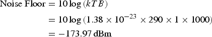
(C) SFDR: It is the range from MDS on the lower side to power compression on the higher side and is given by (1). Noise floor is the theoretical minimum noise for a given bandwidth and temperature. Hence, for a 1 Hz bandwidth at room temperature the noise floor is calculated in (2).
(1)where TOI is input third-order intercept of the link in dB, NF is the noise figure of the link in dB, k is the Boltzman constant, T is the temperature in Kelvin and B is the receiver bandwidth in Hz. $$SFDR = \displaystyle{2 \over 3}(TOI - NF - 10\log \,(kTB)),$$
(2)
$$\eqalign{{\rm Noise}\;{\rm Floor} & = 10\log \,(kTB) \cr & = 10\log \,(1.38 \times {10^{ - 23}} \times 290 \times 1 \times 1000) \cr & = - 173.97\,{\rm dBm}} $$
$$SFDR = \displaystyle{2 \over 3}(TOI - NF - 10\log \,(kTB)),$$
(2)
$$\eqalign{{\rm Noise}\;{\rm Floor} & = 10\log \,(kTB) \cr & = 10\log \,(1.38 \times {10^{ - 23}} \times 290 \times 1 \times 1000) \cr & = - 173.97\,{\rm dBm}} $$
-
(D) MDS: It is minimum input power or the sensitivity of the fiber optic link and is a function of the receiver filter bandwidth and the noise figure of the link. It is designed for 12 dB NF at the frequency of interest using (3). The wider the filter bandwidth at the receiver end, the more thermal noise power will come through it. That in turn would raise the noise floor and make it less sensitive to weak signals.
(3)This implies that any signal greater than −161.97 dBm is detectable on a link with 12 dB NF.
$$\eqalign{MDS & = kTB + NF = - 173.97 + 12 \cr & = - 161.97\,{\rm dBm}.}$$
-
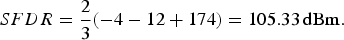
(E) Input TOI: It is typically 8–10 dB higher than the input 1 dB compression point. 1 dB compression point is a measure of components power handling capacity. In this work, the typical value of input 1 dB compression point is −14 dBm as per manufacturer's datasheet, so input TOI is considered at −4 dBm. SFDR is calculated using (1) and is given in (4).
(4)All active devices exhibit non-linearity which results in harmonics and intermodulation products, which may fall within the bandwidth of interest and are hard to filter out because of the proximity to the carriers. Also they grow in power three times faster as 1 dB increase in carrier level causes the third-order products to increase by 3 dB. This system is designed at SFDR of approximately 106 dBm, which implies that with MDS at −161 dBm of the input signal can be well tolerated up to −55 dBm without degraded performance.
$$SFDR = \displaystyle{2 \over 3}( - 4 - 12 + 174) = 105.33\,{\rm dBm}{\rm.} $$
-
(F) Optical power (average) of photodiode: It depends on slope efficiency of photodiode. Slope efficiency represents the transfer function of a laser diode called responsivity. Optical power figure does not play a large role in the fiber optic link performance. For 10 mW optical carrier with 10% modulation index, output power swings between 9 to 11 mW. If the responsivity of photo diode is 0.85 A/W, e.g. the peak to peak current will be 0.00085A. Power output for root-mean-square value of current at matched load of 50 ohm will be −17 dBm. The receiver has about 17 dB RF gain after the photodiode. Thus, the link is zero dB link with pre and post RF amplification.


VI. EXPERIMENTAL SETUP AND RESULTS
Figure 2 shows block diagram of experimental setup and Fig. 3 shows actual photograph of the setup. All optical connectors are cleaned and inspected with optical inspection instrument JDSU P5005i before connection. RF cables are calibrated for all spot frequencies of radar with 0 dBm input power. Testing was carried out in 2–4 GHz band. The link is designed to keep the RF output variation within 0±1 dB for full RF band of 2–4 GHz. Optical power is measured at output of transmitter with optical spectrum analyzer at different wavelengths for all 64 channels. The frequency response of photo diodes is measured with Agilent Spectrum Analyzer PSA E4445A with resolution and video bandwidth of 910 Hz, for all 64 receivers. The measurement at spectrum analyzer was possible with the help of RF gain block circuit present in each receiver module. These values are used to tune the signal conditioning cards at each receiver for specific RF band. The analysis shows that a separate signal conditioning card is required at transmitter and receiver level to equalize the performance for full RF band.

Fig. 2. Block diagram of the experimental setup.

Fig. 3. Actual photograph of the experimental setup.
Variation in received RF power level is observed for all 64 channels due to cascading effect of splitter performance. This restricts interchangeability of receiver modules. The uniformity in the result is possible with the use of 1:64 splitter where channel to channel separation is uniform and fixed. Further a variation of 4 dB is also observed in electrical to optical converter. This variation is compensated with the help of RF signal conditioning cards.
The optical transceivers are designed to operate in linear region only and the output depends on responsivity of photodiode. Figure 4 shows response of optical transceiver for input RF power variation. It can be observed from Fig. 4 that output power level is varying linearly with respect to input power level till 24 dBm, i.e. 10 dB below 1 dB compression point.

Fig. 4. RF response of the optical transceiver.
Microwave photonic link has been analyzed by measuring harmonic distortions to validate proper operation of radar. TOI is an extrapolated point which depends on third-order products and may affect frequency of interest. Harmonic distortion has been measured over full frequency band of 2–4 GHz with a small step size of 100 MHz to analyze this effect. As third-order products are close to carrier, the measurement of harmonic distortion has been carried out upto the fourth level considering that fifth harmonic is small in amplitude [Reference Lin29]. Further the mixers used in receiver for down conversion of frequency are followed by band pass filters; hence, frequencies of the order of fifth and above harmonics, will be rejected by band pass filters. Table 1 shows second, third, and fourth-order components of harmonic distortion. As a design thumb rule, harmonic suppression four times below fundamental signal is considered acceptable. For −14 dBm input RF signal, the second, third, and fourth harmonic should be four times below carrier, i.e. 56 dBc. It can be observed from Table 1 that second, third, and fourth harmonic distortion is <62 dBc. So, it meets the specification of 56 dBc for all spot frequencies of radar.
Table 1. Harmonic distortion of the second, third and fourth orders.

Noise floor has been measured using spectrum analyzer for 2–4 GHz RF band. RG142 RF SMA to SMA cables has been used. Using (2) average noise floor computed for a bandwidth of 2 GHz is −81 dBm. It can be observed from the results presented in Table 2 that it meets the specification required for bandwidth of 2 GHz.
Table 2. Noise floor.

It can be observed form Tables 1 and 2 that harmonic distortion levels are prominent over noise. Each application of RF over fiber requires a specified harmonic level for satisfactory performance [Reference Roselli30]. Radar's dynamic range depends upon receiver's noise and harmonic level. In this work, the transmitter's RF signals are transported over optical fiber; hence degradation in harmonic level does not affect the overall performance of radar, but poses an additional constraint in the form of the reduced operational level available for the transmitter. For radar's proper operation, the harmonic level should be well below the noise level, so that its effect is negligible. This condition is acceptable for transmission path. Same application in receive path will limit the system dynamic range for receive echo.
The link budget is validated against calculations presented in [Reference Mathur, Sridhar and Rai21]. The requirement of same frequency to be split for all digital receivers necessitates for 1:64 splitter, which introduces a loss of 17–20 dB in the system. To compensate for this loss, EDFA is used which is based on automatic light control logic thus keeping PIN diode input constant over varied frequency range. Figure 5 shows the frequency response of the optical distribution network for complete RF band of 2–4 GHz for 0 dBm input RF signal. It can be observed that the variation in output RF power is from −0.4 to +0.7 dB. So, it meets the design objective to limit the variation within ±1 dB.

Fig. 5. Frequency response of the microwave photonic network.
Experimental results in this work have met the specification requirement of digital receivers of the antenna array. The RF signals are verified for faithful reproduction at receiver. It justifies the advantage of microwave photonic network for AESA radar. The production hardware modules are realized to be used with existing radar for field performance.
VII. CONCLUSIONS AND DISCUSSION
Microwave photonic network for RF signal distribution in AESA radar has been designed and validated in this work. The design challenge has been to limit the variation in output RF power to ±1 dB for multiple spot frequencies over the RF band. Since the behavior of RF varies widely over full band, it has been proposed to use different RF signal conditioning cards both at input and output of RF channel with tunable option to limit the variation. Thus, link has been designed to maintain zero dB gain with the help of constant gain EDFA. Proposed microwave photonic network for RF distribution over fiber is modular in nature. This suits the application in AESA radar as AESA radar is also modular with the number of T/R modules depending on radar range. The number of receive modules may be increased to meet the requirements of long-range radars. The proposed microwave photonic network offers an additional advantage of antenna remoting with the help of optical rotary joint. This protects the radar operator from harmful high-power RF radiations. Also it protects the operator and equipments during war time as radar is targetted by sensing its RF radiation. Radar performance is highly dependent on the acceptable levels of non-linear distortion. The experimental results including that of harmonic distortion validates the feasibility of the proposed microwave photonic distribution network for AESA radars offering advantages such as reduced weight, volume, complexity and enhanced data rate, bandwidth, and immunity to EMI and EMC. Further work will be carried out to evaluate the field performance. Future work will be carried out to make the photonic network duplex to reduce the number of cables in the receive path.
 Manisha Mathur received her B.E. degree in Electronics and Communication Engineering from M.I.T.S. Gwalior, India (1990), M. Tech. degree in Digital Communication from M.A.N.I.T. Bhopal, India (1992). Since 1992 she has been working as D.G.M. in Bharat Electronics Limited, Ghaziabad, India. Currently, she leads a team for design and development of active aperture-phased array radar. Her area of interest includes radar signal processing, radar system design, and photonic systems.
 Jaynendra Kumar Rai received his B.E. degree in Electronics Engineering from Shri Guru Gobind Singh College of Engineering and Technology, Nanded, India (1996); M. Tech. degree in Electronics Engineering from Visvesvaraya Regional College of Engineering, Nagpur, India in 1999; and Doctoral degree from Motilal Nehru National Institute of Technology, Deemed University Allahabad, Uttar Pradesh, India in 2011. Presently, he is working as a Professor at the Department of Electronics and Communication Engineering, Amity School of Engineering and Technology, Amity University, Uttar Pradesh, Noida, India. He has published various papers in peer-reviewed international journals and conferences. His current research interests include robotics, medical image and signal processing, and communication engineering.
 Nilakantan Sridhar completed his M.Sc. (in Phy-Electronics) in 1977, M. Phil (in Phy- Microwaves) in 1979, and Ph.D. in Microwave Antenna field in 1983, from the Department of Physics and Astrophysics, University of Delhi. He was involved in the design and realization of many fixed beam, scanning beam antennas for LOS and Satcom applications, Tactical Deployable antennas, Linear and Planar Phased Array antennas for radar applications, etc. Presently, he is working as Addl. General Manager of Qual. Sys. supporting all the manufacturing divisions of Bharat Electronics Ltd., Ghaziabad Unit. He has a number of publications in peer-reviewed international journals and conferences. His current research interests include Microwave Multi beam Antennas, and Active Phased Array Antenna implementations.


