Hostname: page-component-8448b6f56d-42gr6 Total loading time: 0 Render date: 2024-04-20T00:02:45.127Z Has data issue: false hasContentIssue false

Beam-induced atomic migration at Ag-containing nanofacets at an asymmetric Cu grain boundary

Published online by Cambridge University Press:  14 November 2016
Nicolas J. Peter
Affiliation:
Max Planck Institut für Eisenforschung GmbH, Düsseldorf 40237, Germany
Christian H. Liebscher
Affiliation:
Max Planck Institut für Eisenforschung GmbH, Düsseldorf 40237, Germany
Christoph Kirchlechner
Affiliation:
Max Planck Institut für Eisenforschung GmbH, Düsseldorf 40237, Germany
Gerhard Dehm*
Affiliation:
Max Planck Institut für Eisenforschung GmbH, Düsseldorf 40237, Germany
*
a)Address all correspondence to this author. e-mail: dehm@mpie.de
Get access

Abstract

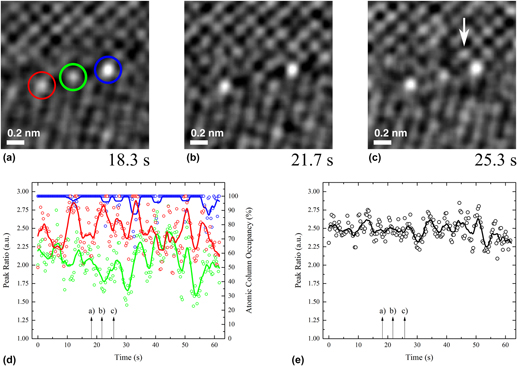
Besides the high spatial resolution achieved in aberration-corrected scanning transmission microscopy, beam-induced dynamic effects have to be considered for quantitative chemical characterization on the level of single atomic columns. The present study investigates the influence of imaging conditions in an aberration-corrected scanning transmission electron microscope on the beam-induced atomic migration at a complex Ag-segregated, nanofaceted Cu grain boundary. Three distinct imaging conditions including static single image and serial image acquisition have been utilized. Chemical information on the Ag column occupation of single atomic columns at the grain boundary was extracted by the evolution of peak intensity ratios and compared to idealized scanning transmission electron microscopy image simulations. The atomic column occupation is underestimated when using conventional single frame acquisition due to an averaging of Ag atomic migration events during acquisition. Possible migration paths for the beam-induced atomic motion at a complex Cu grain boundary are presented.

Type
Articles
Copyright
Copyright © Materials Research Society 2016 

Access options

Get access to the full version of this content by using one of the access options below. (Log in options will check for institutional or personal access. Content may require purchase if you do not have access.)

Footnotes

Contributing Editor: Rafal E. Dunin-Borkowski

References

REFERENCES

Donald, A.M. and Brown, L.M.: Grain boundary faceting in Cu–Bi. Acta Metall. 27(1), 59 (1979).Google Scholar
Duscher, G., Chisholm, M.F., Alber, U., and Ruhle, M.: Bismuth-induced embrittlement of copper grain boundaries. Nat. Mater. 3(9), 621 (2004).Google Scholar
Frolov, T., Divinski, S.V., Asta, M., and Mishin, Y.: Effect of interface phase transformations on diffusion and segregation in high-angle grain boundaries. Phys. Rev. Lett. 110(25), 255502 (2013).CrossRefGoogle ScholarPubMed
Cantwell, P.R., Tang, M., Dillon, S.J., Luo, J., Rohrer, G.S., and Harmer, M.P.: Grain boundary complexions. Acta Mater. 62, 1 (2014).Google Scholar
Chakrabarti, D.J. and Laughlin, D.E.: The Bi–Cu (bismuth–copper) system. Bull. Alloy Phase Diagrams 5(2), 148 (1984).Google Scholar
Chakrabarti, D.J. and Laughlin, D.E.: The B–Cu (boron–copper) system. Bull. Alloy Phase Diagrams 3(1), 45 (1982).Google Scholar
Li, G.H. and Zhang, L.D.: Relationship between misorientation and bismuth induced embrittlement of [001] tilt boundary in copper bicrystal. Scr. Metall. Mater. 32(9), 1335 (1995).Google Scholar
Lozovoi, A.Y. and Paxton, A.T.: Boron in copper: A perfect misfit in the bulk and cohesion enhancer at a grain boundary. Phys. Rev. B: Condens. Matter Mater. Phys. 77(16), 165413 (2008).Google Scholar
Kisielowski, C., Freitag, B., Bischoff, M., Van Lin, H., Lazar, S., Knippels, G., Tiemeijer, P., Van Der Stam, M., Von Harrach, S., Stekelenburg, M., Haider, M., Uhlemann, S., Müller, H., Hartel, P., Kabius, B., Miller, D., Petrov, I., Olson, E.A., Donchev, T., Kenik, E.A., Lupini, A.R., Bentley, J., Pennycook, S.J., Anderson, I.M., Minor, A.M., Schmid, A.K., Duden, T., Radmilovic, V., Ramasse, Q.M., Watanabe, M., Erni, R., Stach, E.A., Denes, P., and Dahmen, U.: Detection of single atoms and buried defects in three dimensions by aberration-corrected electron microscope with 0.5 Å information limit. Microsc. Microanal. 14, 469 (2008).Google Scholar
Wang, Y., Baiutti, F., Gregori, G., Cristiani, G., Salzberger, U., Logvenov, G., Maier, J., and Van Aken, P.A.: Atomic-scale quantitative analysis of lattice distortions at interfaces of two-dimensionally Sr-doped La2CuO4 . ACS Appl. Mater. Interfaces 8, 6763 (2016).Google Scholar
Krivanek, O.L., Dellby, N., Murfitt, M.F., Chisholm, M.F., Pennycook, T.J., Suenaga, K., and Nicolosi, V.: Gentle STEM: ADF imaging and EELS at low primary energies. Ultramicroscopy 110, 935 (2010).CrossRefGoogle Scholar
Egerton, R.F., Li, P., and Malac, M.: Radiation damage in the TEM and SEM. Micron 35, 399 (2004).CrossRefGoogle ScholarPubMed
McBride, J.R., Kippeny, T.C., Pennycook, S.J., and Rosenthal, S.J.: Aberration-corrected Z-contrast scanning transmission electron microscopy of CdSe nanocrystals. Nano Lett. 4(7), 1279 (2004).Google Scholar
Van Aert, S., De Backer, A., Martinez, G.T., Goris, B., Bals, S., Van Tendeloo, G., and Rosenauer, A.: Procedure to count atoms with trustworthy single-atom sensitivity. Phys. Rev. B: Condens. Matter Mater. Phys. 87, 064107 (2013).CrossRefGoogle Scholar
De Backer, A., Martinez, G.T., McArthur, K.E., Jones, L., Béché, A., Nellist, P.D., and Van Aert, S.: Dose limited reliability of quantitative annular dark field scanning transmission electron microscopy for nano-particle atom-counting. Ultramicroscopy 151, 56 (2015).Google Scholar
Van Den Bos, K.H.W., De Backer, A., Martinez, G.T., Winckelmans, N., Bals, S., Nellist, P.D., and Van Aert, S.: Unscrambling mixed elements using high angle annular dark field scanning transmission electron microscopy. Phys. Rev. Lett. 116, 246101 (2016).CrossRefGoogle ScholarPubMed
E, H., McArthur, K.E., Pennycook, T.J., Okunishi, E., D'Alfonso, A.J., Lugg, N.R., Allen, L.J., and Nellist, P.D.: Probe integrated scattering cross sections in the analysis of atomic resolution HAADF STEM images. Ultramicroscopy 133, 109 (2013).CrossRefGoogle ScholarPubMed
Ishikawa, R., Mishra, R., Lupini, A.R., Findlay, S.D., Taniguchi, T., Pantelides, S.T., and Pennycook, S.J.: Direct observation of dopant atom diffusion in a bulk semiconductor crystal enhanced by a large size mismatch. Phys. Rev. Lett. 113, 155501 (2014).Google Scholar
Han, C.W., Iddir, H., Uzun, A., Curtiss, L.A., Browning, N.D., Gates, B.C., and Ortalan, V.: Migration of single iridium atoms and tri-iridium clusters on MgO surfaces: Aberration-corrected STEM imaging and ab initio calculations. J. Phys. Chem. Lett. 6, 4675 (2015).Google Scholar
Bowers, M.L., Ophus, C., Gautam, A., Lançon, F., and Dahmen, U.: Step coalescence by collective motion at an incommensurate grain boundary. Phys. Rev. Lett. 116(10), 106102 (2016).Google Scholar
Yankovich, A.B., Berkels, B., Dahmen, W., Binev, P., Sanchez, S.I., Bradley, S.A., Li, A., Szlufarska, I., and Voyles, P.M.: Picometre-precision analysis of scanning transmission electron microscopy images of platinum nanocatalysts. Nat. Commun. 5, 4155 (2014).Google Scholar
Jones, L.: Quantitative ADF STEM: Acquisition, analysis and interpretation. IOP Conf. Ser.: Mater. Sci. Eng. 109, 012008 (2016).Google Scholar
Subramanian, P.R. and Perepezko, J.H.: The Ag–Cu (silver–copper) system. J. Phase Equilib. 14(1), 62 (1993).Google Scholar
Divinski, S.V., Edelhoff, H., and Prokofjev, S.: Diffusion and segregation of silver in copper Σ5(310) grain boundary. Phys. Rev. B: Condens. Matter Mater. Phys. 85(14), 144104 (2012).Google Scholar
Seah, M.P.: Adsorption-induced interface decohesion. Acta Metall. Mater. 28(7), 955 (1980).Google Scholar
Korzhavyi, P.A., Abrikosov, I.A., and Johansson, B.: Theoretical investigation of sulfur solubility in pure copper and dilute copper-based alloys. Acta Mater. 47(5), 1417 (1999).Google Scholar
LeBeau, J.M., Findlay, S.D., Allen, L.J., and Stemmer, S.: Standardless atom counting in scanning transmission electron microscopy. Nano Lett. 10, 4405 (2010).Google Scholar
Jones, L., Yang, H., Pennycook, T.J., Marshall, M.S.J., Van Aert, S., Browning, N.D., Castell, M.R., and Nellist, P.D.: Smart align—A new tool for robust non-rigid registration of scanning microscope data. Adv. Struct. Chem. Imaging 1, 8 (2015).Google Scholar
Hsieh, W-K., Chen, F-R., Kai, J-J., and Kirkland, A.I.: Resolution extension and exit wave reconstruction in complex HREM. Ultramicroscopy 98, 99 (2004).Google Scholar
Kirkland, E.J.: Advanced Computing in Electron Microscopy, 2nd ed. (Springer, New York, 2010).Google Scholar
Frolov, T., Olmsted, D.L., Asta, M., and Mishin, Y.: Structural phase transformations in metallic grain boundaries. Nat. Commun. 4, 1899 (2013).Google Scholar
Peng, L-M., Ren, G., Dudarev, S., and Whelan, M.: Debye–Waller factors and absorptive scattering factors of elemental crystals. Acta Crystallogr., Sect. A: Found. Crystallogr. 52(3), 456 (1996).CrossRefGoogle Scholar
Grønlund, F. and Moore, W.J.: Sputtering of silver by light ions with energies from 2 to 12 keV. J. Chem. Phys. 32(5), 1540 (1960).Google Scholar
Robb, P.D. and Craven, A.J.: Column ratio mapping: A processing technique for atomic resolution high-angle annular dark-field (HAADF) images. Ultramicroscopy 109(1), 61 (2008).Google Scholar
Pennycook, S.J.: Z-Contrast transmission electron microscopy: Direct atomic imaging of materials. Annu. Rev. Mater. Sci. 22(1), 171 (1992).Google Scholar
Wang, Z.W., Li, Z.Y., Park, S.J., Abdela, A., Tang, D., and Palmer, R.E.: Quantitative Z-contrast imaging in the scanning transmission electron microscope with size-selected clusters. Phys Rev B 84(7), 073408 (2011).Google Scholar
Ishizuka, K.: A practical approach for STEM image simulation based on the FFT multislice method. Ultramicroscopy 90(2–3), 71 (2002).Google Scholar
Ma, Q., Liu, C.L., Adams, J.B., and Balluffi, R.W.: Diffusion along [001] tilt boundaries in the Au/Ag system—II. Atomistic modeling and interpretation. Acta Metall. Mater. 41(1), 143 (1993).CrossRefGoogle Scholar
Mishin, Y., Herzig, C., Bernardini, J., and Gust, W.: Grain boundary diffusion: Fundamentals to recent developments. Int. Mater. Rev. 42(4), 155 (1997).Google Scholar
File 24 MB
Supplementary material: Image

Peter supplementary material

Fig. S1

Download Peter supplementary material(Image)
Image 529.4 KB
Supplementary material: Image

Peter supplementary material

Fig. S2

Download Peter supplementary material(Image)
Image 516.9 KB
Supplementary material: Image

Peter supplementary material

Fig. S3

Download Peter supplementary material(Image)
Image 1.1 MB
Supplementary material: File

Peter supplementary material

Peter supplementary material 1

Download Peter supplementary material(File)
File 12.1 KB

Peter supplementary material

Audio

Download Peter supplementary material(Video)
Video 28.4 MB