


Introduction
In 2004, the state-of-the-art technique for realizing atomically thin materials consisted of a roll of tape and a layered crystal held together by van der Waals forces [Reference Novoselov, Geim, Morozov, Jiang, Katsnelson, Grigorieva, Dubonos and Firsov1, Reference Novoselov, Jiang, Schedin, Booth, V Khotkevich, V Morozov and Geim2]. The so-called scotch-tape exfoliation method enabled isolation of molecularly thin layers from dozens of van der Waals [also known as two-dimensional (2D)] materials such as molybdenum disulfide (MoS2), tungsten diselenide (WSe2), and hexagonal boron nitride (hBN) [Reference Novoselov, Jiang, Schedin, Booth, V Khotkevich, V Morozov and Geim2, Reference Geim and Grigorieva3]. On realizing the promise of 2D materials (2DMs) for use in next-generation technologies, the community quickly advanced beyond micrometer-sized flakes of 2D layers produced by the scotch-tape method and toward the realization of continuous films over large-area substrates (up to 300 mm diameter SiO2/silicon) [Reference Kang, Xie, Huang, Han, Huang, Mak, Kim, Muller and Park4, Reference Lin, Jariwala, Bersch, Xu, Nie, Wang, Eichfeld, Zhang, Choudhury, Pan, Addou, Smyth, Li, Zhang, Haque, Fölsch, Feenstra, Wallace, Cho, Fullerton-Shirey, Redwing and Robinson5, Reference Zhang, Choudhury, Chubarov, Xiang, Jariwala, Zhang, Alem, Wang, Robinson and Redwing6, Reference Eichfeld, Hossain, Lin, Piasecki, Kupp, Birdwell, Burke, Lu, Peng, Li, Azcatl, McDonnell, Wallace, Kim, Mayer, Redwing and Robinson7, Reference Jeong, Kim, Kim, Moon, Han, Lee, Okello, Song, Choi and Kim8, Reference Robertson, Liu, Yue, Escarra and Wei9], all enabled by simple vapor deposition techniques [Reference Briggs, Subramanian, Lin, Li, Zhang, Zhang, Xiao, Geohegan, Wallace, Chen, Terrones, Ebrahimi, Das, Redwing, Hinkle, Momeni, van Duin, Crespi, Kar and Robinson10]. The most rudimentary of these techniques utilizes a tube furnace–based approach, including solid source precursors and, more recently, nucleation or seeding agents that can yield 2D films over large areas [Reference Kang, Xie, Huang, Han, Huang, Mak, Kim, Muller and Park4, Reference Kim, Ovchinnikov, Deiana, Unuchek and Kis11, Reference Ling, Lee, Lin, Fang, Yu, Dresselhaus and Kong12, Reference Huang, Liang, Ling, Puretzky, Geohegan, Sumpter, Kong, Meunier and Dresselhaus13]. The beauty of this approach lies in its logistical simplicity—one can merely heat source powders and substrates together in a tube furnace to achieve rapid synthesis of large-area 2D films in nearly any laboratory. This enables researchers to investigate fundamental material properties, basic physics, and proof-of-concept devices with only a small barrier to creating the films themselves [Reference Briggs, Subramanian, Lin, Li, Zhang, Zhang, Xiao, Geohegan, Wallace, Chen, Terrones, Ebrahimi, Das, Redwing, Hinkle, Momeni, van Duin, Crespi, Kar and Robinson10]. Following deposition, 2D films are commonly characterized via Raman, photoluminescence (PL), and X-ray photoelectron spectroscopies, which can be used to determine film composition, layer number, and band gap. Despite the ease of these deposition and characterization techniques, some limitations exist in their application to 2DMs [Reference Briggs, Subramanian, Lin, Li, Zhang, Zhang, Xiao, Geohegan, Wallace, Chen, Terrones, Ebrahimi, Das, Redwing, Hinkle, Momeni, van Duin, Crespi, Kar and Robinson10]. Here, we highlight commonly overlooked scientific details of 2DMs synthesis and characterization that can ultimately impact scientific claims, with focus on solid-source and seed-promoted deposition, as well as Raman, PL, and X-ray photoelectron spectroscopic characterization.
Chemical vapor deposition of 2-dimensional materials
Solid-source chemical vapor deposition
The rapid development of the field of 2DMs synthesis research has been possible due to its relatively low cost of entry. For only a few thousand dollars, solid source precursors such as sulfur, tungsten-oxide, and molybdenum-oxide powders, and commonly available inventory, one can set up a simple tube furnace and begin growing 2DMs. While this tube furnace infrastructure dominates 2DM synthesis research today [Reference Cai, Liu, Zou and Cheng14, Reference Zhang and Fu15, Reference Bhimanapati, Lin, Meunier, Jung, Cha, Das, Xiao, Son, Strano, Cooper, Liang, Louie, Ringe, Zhou, Kim, Naik, Sumpter, Terrones, Xia, Wang, Zhu, Akinwande, Alem, Schuller, Schaak, Terrones and Robinson16], realization of truly repeatable, high-quality synthetic 2DMs requires significant modifications to solid-source (S) chemical vapor deposition (CVD) processes or completely different syntheses approaches. This is due to the poor reproducibility of S-CVD synthesis recipes, which often vary widely between furnaces and even between individual researchers in a single laboratory. Several variables of paramount importance can easily be overlooked during S-CVD processes, such as reactor and crucible geometry, furnace heating and cooling rates [Reference Momeni, Ji, Zhang, Robinson and Chen17, Reference Zhang, Momeni, AlSaud, Azizi, Hainey, Redwing, Chen and Alem18], and substrate cleaning or surface preparation [Reference Lin, Jariwala, Bersch, Xu, Nie, Wang, Eichfeld, Zhang, Choudhury, Pan, Addou, Smyth, Li, Zhang, Haque, Fölsch, Feenstra, Wallace, Cho, Fullerton-Shirey, Redwing and Robinson5]. These variables are often unreported or overlooked in the literature, with many researchers claiming S-CVD to be a viable technique for uniform, large-scale 2DM synthesis. While some studies demonstrate quasi-uniform deposition on centimeter-scale samples, scaling to industrially relevant substrate sizes (>200 mm) using S-CVD is unlikely. Similarly, 2DM literature contains little mention of reactor “seasoning” or the effects of precursor buildup on crucibles and the interior of quartz tubes when S-CVD is utilized. This buildup significantly impacts material growth in hot wall S-CVD studies because it leads to a continuously changing partial pressure of precursors with each additional run, making every run unique [Reference Hampden‐Smith and Kodas19]. Beyond incomplete reporting of reactor and process details in 2DM S-CVD literature, S-CVD offers little control over precursor materials or concentration at the substrate surface. One commonly observed consequence of the horizontal tube furnace–based S-CVD approach is a deposition plume [Figs. 1(a) and 1(b)], containing a gradient of 2D layer domain morphologies across the substrate surface. The quintessential triangular monolayer is often only observed only in a specific region of this deposition plume [Fig. 1(c)], due to variation in the precursor concentration across the substrate surface, and as a result, varying 2D crystal edge terminations and growth rates [Reference Wang, Rong, Fan, Pacios, Bhaskaran, He and Warner20]. Control over precursor concentration in S-CVD studies is primarily achieved by varying source temperature and distance from substrate [Reference Wang, Rong, Fan, Pacios, Bhaskaran, He and Warner20].

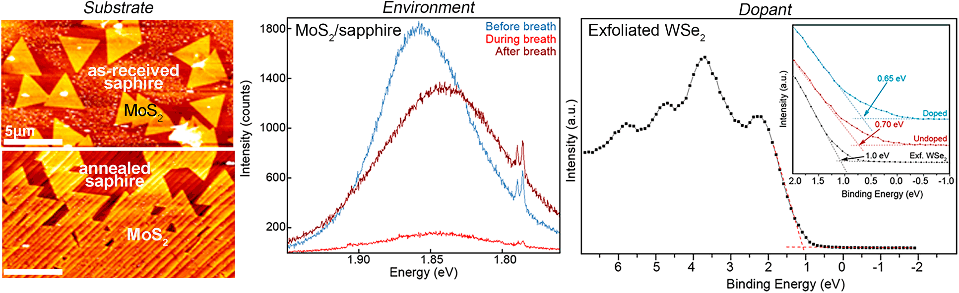
Figure 1: (a)–(c) MoS2 grown on SiO2/Si via S-CVD. (a) A typical MoS2 deposition plume, which can be divided into regions of varying MoS2 morphologies (b). (c) Scanning electron microscope images of these regions. (d) The as-received c-plane sapphire. (e) c-plane sapphire annealed at 1150 °C for 8 h in ambient, resulting in the formation of terraces. (f) S-CVD-grown MoS2 on as-received sapphire showing no domain orientation. (g) S-CVD-grown MoS2 on annealed sapphire showing orientation of domains. (a)–(c) reproduced with permission from Ref. Reference Wang, Rong, Fan, Pacios, Bhaskaran, He and Warner20.
While S-CVD is a common technique for rapid realization of millimeter-scale 2DMs, the complexity of tube furnace–based S-CVD can lead to poor reproducibility even between personnel within a single research group. Therefore, process parameters reported for S-CVD techniques should be viewed merely as qualitative guidelines, where reported recipes are not likely to directly translate between laboratories but can serve as a valuable starting point for 2DM synthesis studies. One effort to reduce variability in S-CVD of 2DMs lies in computational investigations to understand flow patterns and precursor concentration variation at substrates surfaces [Reference Momeni, Ji, Zhang, Robinson and Chen17, Reference Zhang, Momeni, AlSaud, Azizi, Hainey, Redwing, Chen and Alem18, Reference Xuan, Jain, Zafar, Lotfi, Nayir, Wang, Choudhury, Wright, Feraca, Rosenbaum, Redwing, Crespi and van Duin21]. While these efforts are relatively few, they can greatly aid understanding of the requirements for 2DM growth. Beyond S-CVD growth of 2DMs, it is important to consider the use of alternative gas source deposition methods, such as atomic layer deposition [Reference Hao, Marichy and Journet22], traditional CVD [Reference Kang, Xie, Huang, Han, Huang, Mak, Kim, Muller and Park4], and metal organic (MO) CVD [Reference Briggs, Subramanian, Lin, Li, Zhang, Zhang, Xiao, Geohegan, Wallace, Chen, Terrones, Ebrahimi, Das, Redwing, Hinkle, Momeni, van Duin, Crespi, Kar and Robinson10], which offer controllable introduction of precursors into the reactors. Such techniques may require greater initial capital but can yield highly reproducible results and uniform, large-area 2D films. Efforts to achieve large-area films of 2DMs have matured in recent years, with demonstrations of coalesced films of transition metal dichalcogenides (TMDs) like tungsten diselenide (WSe2) and MoS2 grown over centimeter scales [Reference Kang, Xie, Huang, Han, Huang, Mak, Kim, Muller and Park4, Reference Lin, Jariwala, Bersch, Xu, Nie, Wang, Eichfeld, Zhang, Choudhury, Pan, Addou, Smyth, Li, Zhang, Haque, Fölsch, Feenstra, Wallace, Cho, Fullerton-Shirey, Redwing and Robinson5, Reference Zhang, Choudhury, Chubarov, Xiang, Jariwala, Zhang, Alem, Wang, Robinson and Redwing6, Reference Eichfeld, Hossain, Lin, Piasecki, Kupp, Birdwell, Burke, Lu, Peng, Li, Azcatl, McDonnell, Wallace, Kim, Mayer, Redwing and Robinson7]. These large-area films have been possible through the use of MOCVD, where the concentration and ratios of metal and chalcogen species can be precisely controlled via bubblers, and sequential nucleation and ripening steps may be performed to control TMD domain sizes and layer number [Reference Lin, Jariwala, Bersch, Xu, Nie, Wang, Eichfeld, Zhang, Choudhury, Pan, Addou, Smyth, Li, Zhang, Haque, Fölsch, Feenstra, Wallace, Cho, Fullerton-Shirey, Redwing and Robinson5, Reference Zhang, Choudhury, Chubarov, Xiang, Jariwala, Zhang, Alem, Wang, Robinson and Redwing6].
Beyond the use of gas source deposition methods, substrate pretreatment can be used to control 2DM growth. This is shown in both MOCVD and S-CVD [Figs. 1(d)–1(g)] studies of TMD growth on c-plane sapphire [Reference Wang, Rong, Fan, Pacios, Bhaskaran, He and Warner20]. While many 2DM synthesis studies utilize SiO2/Si substrates, c-plane sapphire is an increasingly popular substrate, due to potential for aligned 2DM domains resulting from long-range commensurability with sapphire [Reference Lin, Jariwala, Bersch, Xu, Nie, Wang, Eichfeld, Zhang, Choudhury, Pan, Addou, Smyth, Li, Zhang, Haque, Fölsch, Feenstra, Wallace, Cho, Fullerton-Shirey, Redwing and Robinson5, Reference Zhang, Choudhury, Chubarov, Xiang, Jariwala, Zhang, Alem, Wang, Robinson and Redwing6, Reference Eichfeld, Hossain, Lin, Piasecki, Kupp, Birdwell, Burke, Lu, Peng, Li, Azcatl, McDonnell, Wallace, Kim, Mayer, Redwing and Robinson7, Reference Zhang, Borys, Bersch, Bhimanapati, Xu, Wang, Wang, Labella, Williams, Haque, Barnard, Fullerton-Shirey, Schuck and Robinson23]. Direct growth of 2DMs on as-received c-plane sapphire, however, may not be sufficient in achieving oriented 2DM domains from S-CVD growth. Annealing sapphire to reduce the contact angle of the substrates is shown to enable dramatic improvement in domain orientation due to the formation of terraces in the sapphire surface, which promote certain domain orientations [Figs. 1(d)–1(g)] [Reference Lin, Jariwala, Bersch, Xu, Nie, Wang, Eichfeld, Zhang, Choudhury, Pan, Addou, Smyth, Li, Zhang, Haque, Fölsch, Feenstra, Wallace, Cho, Fullerton-Shirey, Redwing and Robinson5, Reference Zhang, Borys, Bersch, Bhimanapati, Xu, Wang, Wang, Labella, Williams, Haque, Barnard, Fullerton-Shirey, Schuck and Robinson23, Reference Dumcenco, Ovchinnikov, Marinov, Lazić, Gibertini, Marzari, Sanchez, Kung, Krasnozhon, Chen, Bertolazzi, Gillet, Fontcuberta i Morral, Radenovic and Kis24]. The use of c-plane sapphire as a substrate for epitaxial growth has enabled understanding of the requirements for lateral growth of domains and control of nominal layer number [Reference Zhang, Choudhury, Chubarov, Xiang, Jariwala, Zhang, Alem, Wang, Robinson and Redwing6]. Observation of this domain orientation in both S-CVD and MOCVD studies reveals that substrate engineering can be an effective strategy to control the orientation and growth of 2D layers.
Seed-promoted CVD
In addition to the use of MOCVD for large-area 2DM growth, nucleation agents and seeding techniques have gained traction as tools to achieve increased 2DM domain sizes [Reference Kang, Xie, Huang, Han, Huang, Mak, Kim, Muller and Park4, Reference Kim, Ovchinnikov, Deiana, Unuchek and Kis11, Reference Ling, Lee, Lin, Fang, Yu, Dresselhaus and Kong12, Reference Huang, Liang, Ling, Puretzky, Geohegan, Sumpter, Kong, Meunier and Dresselhaus13, Reference Zhang, Jariwala, Li, Briggs, Wang, Ruzmetov, Burke, Lerach, Ivanov, Haque, Feenstra and Robinson25]. Kang et al. [Reference Kang, Xie, Huang, Han, Huang, Mak, Kim, Muller and Park4] popularized the use of alkali-based compounds (e.g., NaCl) to achieve large-domain 2D TMD layers via MOCVD, and the approach has since been expanded to a large library of 2D layers grown via S-CVD [Reference Zhou, Lin, Huang, Zhou, Chen, Xia, Wang, Xie, Yu, Lei, Wu, Liu, Fu, Zeng, Hsu, Yang, Lu, Yu, Shen, Lin, Yakobson, Liu, Suenaga, Liu and Liu26]. While salt-assisted growth does result in large-area TMD films with fewer grain boundaries, recent studies show Na atoms present at the TMD/substrate interface, which can lead to variation in coupling between the growth substrate and TMD layers. This causes spatial variation in electronic properties of the grown TMD [Reference Zhang, Bersch, Zhang, Briggs, Subramanian, Xu, Chubarov, Wang, Lerach, Redwing, Fullerton-Shirey, Terrones and Robinson27]. Such variations in coupling can also affect the quality of the grown material significantly, resulting in a tensile strain in the layers and a reduction of the PL intensity of MoS2 layers by roughly 100×. Furthermore, these studies indicate that while NaCl may serve to control nucleation and promote large area growth of MoS2, NaCl can also degrade the electrical performance of these grown semiconducting layers even when the films are transferred from the growth substrate [Reference Zhang, Bersch, Zhang, Briggs, Subramanian, Xu, Chubarov, Wang, Lerach, Redwing, Fullerton-Shirey, Terrones and Robinson27]. More importantly, however, is the 50+ years of research in the semiconductor industry that provides overwhelming evidence that the presence of alkali ions leads to higher oxide leakage currents and reliability problems in semiconductor devices when operated at high temperatures and voltages [Reference Hefley and McPherson28, Reference Schjølberg-Henriksen, Jensen, Hanneborg and Jakobsen29, Reference Lycoudes and Childers30, Reference Kuhn and Silversmith31, Reference Snow, Grove, Deal and Sah32, Reference Constant, Tardif and Derrien33].
This was demonstrated by Snow et al. [Reference Snow, Grove, Deal and Sah32] in 1965 (Fig. 2) through nonuniform shifts in capacitance–voltage (C–V) curves in a Na-contaminated metal–oxide–silicon (MOS) capacitor. The oxide leakage currents observed in the MOS structures are associated with the drift in C–V curves. The ionic drift within the oxide leads to significant shifts in the silicon charge, where upon application of a positive bias at 150 °C for 5 min, a >100 V bias shift in the C–V curve occurs [Fig. 2(a)], corresponding to a buildup of negative charge. This shift is independent of substrate doping. When Na and other alkali ions are not present in the MOS capacitors, the C–V curves do not drift. As shown in Fig. 2(b), alkali-contaminated devices can also exhibit more complicated C–V curves after drift. These distorted curves are caused by nonuniform alkali contamination over the surface of the device, causing some areas to drift more than others, leading to adjacent devices displaying different characteristics. Considering many integrated circuits operate between 55 and 85 °C, one can expect significant diffusion of alkali ions and reduced transistor stability if such ions are present, even at low concentrations. Any commercial semiconductor fabrication facility will strongly object to a process that utilizes any alkali ion–based process, indicating that alkali ions must be avoided at all cost when considering 2DMs for augmenting semiconductor technology for complimentary metal-oxide-semiconductor (CMOS) applications. Other applications including low power devices for Internet of Things technology and 2DM-based chemical and biological sensors may have a higher tolerance for these mobile ions.

Figure 2: (a) C–V curves of an MOS structure with sodium contamination at the metal/oxide interface. The high diffusion rates of Na through the oxide under electrical bias lead to severe shifts in the CV curves, demonstrating significant device instability due to alkali ions. (b) C–V curves showing the more complicated curves due to nonuniform contamination over the surface of the device. Reproduced with permission from Ref. Reference Snow, Grove, Deal and Sah32.
Spectroscopic characterization of 2D materials
Raman and PL spectroscopies
Detailed investigation of the quality of synthesized 2DMs requires a technique that examines the sample on an appropriate length scale and provides relevant structural or chemical information. Raman and PL spectroscopies are excellent characterization tools for 2DMs because they require little to no sample preparation and provide a wealth of information within short acquisition times [Reference Wu, Lin, Cong, Liu and Tan34, Reference Zhang, Tan, Wu, Shi and Tan35, Reference Zhang, Qiao, Shi, Wu, Jiang and Tan36, Reference Lee and Cheong37]. However, this extensive information can be easily misinterpreted if one is inexperienced in spectral analysis of inelastic scattering in 2DMs. One commonly misinterpreted result of spectral (Raman and PL) data relates to the identification of the number of layers in 2DMs. Generally, this misinterpretation is a result of limited spectral analysis and an unawareness that certain spectral features can be affected by factors unrelated to layer number (Fig. 3).

Figure 3: (a) E2g and A1g modes of MoS2, which shift with increasing MoS2 layer number. (b) Peak shift of E12g and A1g modes in strained MoS2. The E12g mode shifts to higher wavenumber when compressed and shifts to lower wavenumber under tension. (c) Theoretical calculations and experimental measurements of MoS2 E12g and A1g peak shifts due to increasing sulfur vacancy %. (d) Changes in MoS2 E12g and A1g positions as a function of carrier concentration. (e) THz Raman measurements of MoS2, showing changes in the spectral region below 50 cm−1 as a function of MoS2 layer number. (f) MoS2 PL as a function of MoS2 thickness (1.3–7.6 nm). (a)–(f) Reproduced with permission from Refs. Reference Li, Zhang, Yap, Tay, Edwin, Olivier and Baillargeat38, Reference Wang, Cong, Qiu and Yu39, Reference Parkin, Balan, Liang, Das, Lamparski, Naylor, Rodríguez-Manzo, Johnson, Meunier and Drndić40, Reference Chakraborty, Bera, Muthu, Bhowmick, Waghmare and Sood41, Reference Lee, Woo, Park, Park, Son and Cheong42, and Reference Pham, Li, Bekyarova, Itkis and Mulchandani44.
The most common method of reporting 2DM layer number is via Raman spectroscopy, based on the spectral separation of the E12g and A1g vibrational modes in MoS2 [Fig. 3(a)], which increases with increasing layer number [Reference Li, Zhang, Yap, Tay, Edwin, Olivier and Baillargeat38]. This approach is challenging due to the factors such as film strain [Fig. 3(b)] [Reference Wang, Cong, Qiu and Yu39], concentration of sulfur vacancies [Fig. 3(c)] [Reference Parkin, Balan, Liang, Das, Lamparski, Naylor, Rodríguez-Manzo, Johnson, Meunier and Drndić40], and electronic carrier concentrations [Fig. 3(d)] [Reference Chakraborty, Bera, Muthu, Bhowmick, Waghmare and Sood41]—all of which impact the absolute spacing between E2g and A1g in MoS2. Some of these characteristics like sulfur vacancy concentration can change with time or environment, whereas others like strain and carrier concentration are predominantly determined by the growth conditions. There are a few additional ways to utilize Raman for identifying 2D layer number, as noted in Fig. 3(e). Given access to a Raman spectrometer with ultra-low frequency Rayleigh filters and thus the ability to analyze THz frequencies (approximately spectral regions below 50 cm−1), one may use THz modes to confirm 2DM layer number. Raman peaks in this spectral range for van der Waals materials are associated with shear [C in Fig. 3(e)] and layer breathing [LB in Fig. 3(e)] modes and are therefore the most direct way of counting the number of 2D layers [Reference Lee, Woo, Park, Park, Son and Cheong42]. In addition, the THz bands are less susceptible to peak shift as a function of strain [Reference Eda, Yamaguchi, Voiry, Fujita, Chen and Chhowalla43].
Another approach to layer number measurement—often more accessible than THz Raman—is the measurement of 2DM PL. Semiconducting monolayer TMDs typically exhibit an optical band gap in the visible spectrum. Measuring the PL of these materials requires the use of an excitation laser energy that is above the semiconductor optical band gap and a spectrometer that enables access to the PL energy [Fig. 3(f)]. Most research-grade Raman spectrometers match these conditions for MoS2, which has an indirect band gap of ∼1.3 eV in bulk and a direct band gap of ∼1.8 eV at monolayer thickness. Therefore, the PL peak position of MoS2 may be used as an additional indication of the layer number [Reference Pham, Li, Bekyarova, Itkis and Mulchandani44]. However, the PL response of the monolayer material is so sensitive that the peak rapidly and dynamically evolves in response to the environment—even when one merely breathes onto the sample (Fig. 4). Molecules adsorbed onto MoS2 layers from breathing onto the surface change the electronic band structure of the MoS2. One breath onto the sample changes the PL peak position by 20 meV. This peak position change is greater than that between MoS2 flakes with thicknesses of 1.3 and 7.6 nm, as shown in Fig. 3(f) [Reference Pham, Li, Bekyarova, Itkis and Mulchandani44]. This “breath” experiment highlights the importance of understanding sample history and the environmental considerations when utilizing PL for quantification of layer thickness. Conversely, many groups have investigated the PL response of 2DMs as chemical sensors, leveraging this surface sensitivity while considering irradiation effects from the excitation laser [Reference Akbari, Jahanbin, Afroozeh, Yupapin and Buntat45, Reference Chambers, Droubay, Kaspar and Gutowski46].

Figure 4: (a) PL response (highlighted in gray) of monolayer MoS2 as a result of a student breathing on the sample with “minty fresh breath.” The PL peak position (△) decreases after the breath event (shaded region) and the FWHM (○) increases. (b) Selected PL peaks at the time interval just before the breath event, during the breath, and ∼35 s after the breath. The doublet around 1.79 eV is a result of Cr 3+ in the sapphire substrate.
X-ray photoelectron spectroscopy
In addition to Raman and PL, X-ray photoelectron spectroscopy (XPS) can serve as a valuable 2DM characterization technique. XPS provides direct evidence of elemental bonding at the surfaces of materials, making it attractive for understanding the composition of 2DMs. This technique has a unique combination of attributes that align particularly well with 2DMs, including surface sensitivity, accurate quantification with little or no matrix effects, sensitivity to every element in the periodic table except H and He, and the ability to determine the nearest neighbor chemical environment in many instances. This technique is commonly used in the 2DM field to investigate chemistry and stoichiometry in 2DMs, as well as dopant concentrations and impacts on valence band maxima (VBMs). To effectively utilize XPS for investigation of 2DMs, several considerations regarding stoichiometry and valence band measurements must be made.
Perhaps the attribute that XPS is best known for is its ability to determine the nearest neighbor chemical environment. The binding energy of core electrons emitted and detected via XPS is affected by formal valence state and other differences in chemical environment. Thus, XPS can be used to explore surface and interfacial reactions between 2DMs and to investigate relative elemental composition. Figure 5 shows a typical spectrum of WSe2 grown on sapphire (Al2O3), where W, Se, Al, and O peaks are clearly evident. The inset shows high-resolution spectra of the W 4f and Se 3d regions, and the measured Se:W ratio is found to be 1.96 (close to the expected 2.0). As a check of repeatability and accuracy of these measurements, a series of bulk 2DMs were repeatedly exfoliated and measured for composition (for flakes with acceptably low levels of C and O contamination). The standard deviation of the chalcogen-to-metal ratio varied by <2% for the TMDs MoS2, WS2, WSe2, and the layered material Bi2Te3. The actual standard deviation of thin 2DMs on substrates is expected to be worse due to lower signal strength but will remain <5%.

Figure 5: XPS spectra collected for WSe2 grown on sapphire. W, Se, Al, and O peaks are indicated. High-resolution spectra (inset) show Se and W with a Se:W ratio of 1.96. This measured ratio may deviate significantly from the true Se:W ratio, as found from additional studies of exfoliated WSe2. These studies suggest that RSF derivation from references samples is required for accurate XPS analysis of 2DMs.
The accuracy of these measured stoichiometries, however, is another matter entirely. In all cases, the bulk material composition and crystal chemistry were confirmed using X-ray fluorescence and X-ray diffraction, respectively. The XPS-measured stoichiometries of MoS2 and WS2 were within 3% of the true values. However, when this same methodology was applied to WSe2, the Se:W ratio was 1.69 instead of 2.00, a 16% error. The Te:Bi ratio on Bi2Te3 was 1.19 instead of 1.50. These results, obtained under ideal conditions, should provide a cautionary tale that determining the absolute stoichiometry of 2DMs may require derivation of relative sensitivity factors (RSFs) from reference samples rather than relying on RSFs supplied by the XPS instrument vendor. Under the best conditions of a continuous thin film of MoS2 on a substrate with no interfering peaks, the 2σ standard deviation (95% confidence interval) of XPS-measured stoichiometry suggests that the best that can be achieved is MoS2.0±0.1 (5%). Therefore, one should avoid claims of a stoichiometric 2DM based on XPS, as the error is likely 3–5%—a variation large enough to dramatically affect the optical and electronic properties.
Beyond measuring the stoichiometry of 2DMs, there is intense interest in doping 2DMs to alter their electronic properties [Reference Briggs, Subramanian, Lin, Li, Zhang, Zhang, Xiao, Geohegan, Wallace, Chen, Terrones, Ebrahimi, Das, Redwing, Hinkle, Momeni, van Duin, Crespi, Kar and Robinson10]. XPS is ideal for understanding the bonding environment of the dopants (e.g., dopant bonding to chalcogen or transition metal) but can also shed light on how the dopant impacts the electronic structure via measurement of VBMs. While the data used to identify bonding in XPS are based on core electrons, weakly bound valence electrons are also accessible. Measurements of the VBM can be combined with careful core level measurements to yield valence band offsets, which are important for understanding and predicting potential heterojunctions in 2D devices [Reference Chiu, Zhang, Shiu, Chuu, Chen, Chang, Chen, Chou, Shih and Li47, 48]. However, the X-ray cross section of these electrons is typically quite low, resulting in weak XPS signals [Fig. 6(a)]. This is evident from the spectra acquired from V-doped WS2 on SiO2 [Fig. 6(a)]. The sum of W, S, and V signals from this sample is <7% of the total signal, and nearly 90% of the signal originates from the SiO2 substrate (with the balance coming from adsorbed organics). Furthermore, the V 2p 3/2 spectra of undoped, lightly doped, and highly doped WS2 [Fig. 6(a), inset] show evidence of multiple chemical states, requiring curve fitting into three overlapping components despite the fact that there is <0.3% total vanadium present. The peak at 513.5 eV is due to VSx species with the higher binding energy peaks due to various oxides of vanadium. The lightly doped sample exhibits a W:V of ∼41, while the more heavily doped sample has a ratio of 7.7. In addition to these weak XPS signals, when films are placed on dielectric substrates, there is inevitable substrate charging that must be accounted for.

Figure 6: (a) XPS spectra of V-doped WS2 on sapphire. SiO2 signal dominates the spectra, accounting for 90% of the acquired signal. <7% of the signal originates from W, S, and V. The inset in (a) shows the V region for (a, i) undoped, (a, ii) lightly doped (W:V = 41), and (a,iii) highly doped (W:V = 7.7) WS2. (a, iii) shows multiple chemical states of V. (b) VBM of exfoliated and Re-doped (inset) WSe2. The measured valence band offset shown in the inset is found to be statistically insignificant with follow-up measurements. All spectra are charged referenced to W 4f 7/2 in WSe2 at 32.70 eV.
When determining VBMs in XPS, care must be taken to ensure that the acquired data are statistically significant. This is exemplified in Fig. 6(b), which shows measured VBMs for Re-doped (W:Re = 4) and undoped WSe2 grown on sapphire. Freshly exfoliated bulk WSe2 is also shown for comparison. This provides a prime example of how Se vacancies can also lead to shifting in the VBM, even in undoped samples, where there is a 0.3 eV shift between exfoliated WSe2 grown via chemical vapor transport and MOCVD grown WSe2 (undoped). The VBM is typically determined by finding the intersection of two linear fits of background near 0 eV and the near-linear portion of the leading edge of the valence band [Fig. 6(b) inset]. Through this approach, a very small (0.05 eV) difference is found between the doped and undoped WSe2 [Fig. 6(b)]. However, repeated measurements (n = 4) reveal that these values are not statistically different. By employing high-energy resolution scans with signal-to-noise ratio >30:1, careful charge correction and careful fitting, a 2σ standard deviation ±0.10 eV, can be achieved. Thus, researchers must take care to acquire sufficiently precise and statistically significant measurements when investigating doping and VBM in 2DMs as the noise levels in these measurements can be much greater than the shifts themselves.
Conclusion
This article accumulates commonly overlooked scientific details in the synthesis and characterization 2DMs, with a focus on TMDs. It is intended to be used as a cautionary guide for researchers working in vapor-phase synthesis and spectroscopic characterization of 2DMs. Specifically, researchers should be aware of variability associated with S-CVD-grown materials and potential influences of nucleation agents on the properties of the synthesized 2DMs. When characterizing grown 2DMs, an understanding of the impacts of growth conditions and the local environment is crucial. Furthermore, reporting of 2DM layer number and stoichiometry must be done with caution if Raman and XPS techniques are used, and statistical significance of VBM measurements should be reported. As the 2DM field continues to progress, synthesis and characterization details must be scrutinized and communicated to researchers in the field at large to ensure consensus in scientific reporting and drawn conclusions.
Acknowledgments
S.S. and J.A.R. acknowledge the funding from NSF CAREER (Award: 1453924). N.B. and J.A.R. acknowledge the funding for this work that was provided by the Northrop Grumman Mission Systems' University Research Program, Semiconductor Research Corporation Intel/Global Research Collaboration Fellowship Program, task 2741.001, Pennsylvania State University Materials Research Institute's Material Characterization Laboratory. The authors would like to thank Dr. Kehao Zhang whose research results have been used in Figs. 1(d)–1(g). The authors would also like to acknowledge Azimkhan Kozhakmetov, Dr. Fu Zhang, and Prof. Mauricio Terrones who provided the samples for XPS measurements.


 Open access