Hostname: page-component-848d4c4894-wzw2p Total loading time: 0 Render date: 2024-05-01T17:42:30.941Z Has data issue: false hasContentIssue false

Effect of LPHT annealing on interface characteristics between HPHT Ib diamond substrates and homoepitaxial CVD diamond layers

Published online by Cambridge University Press:  17 January 2020

Xiaohua Zhu
Affiliation:
Institute for Advanced Materials and Technology, University of Science and Technology Beijing, Beijing 100083, People's Republic of China
Jinlong Liu*
Affiliation:
Institute for Advanced Materials and Technology, University of Science and Technology Beijing, Beijing 100083, People's Republic of China
Siwu Shao
Affiliation:
Institute for Advanced Materials and Technology, University of Science and Technology Beijing, Beijing 100083, People's Republic of China
Yun Zhao
Affiliation:
Institute for Advanced Materials and Technology, University of Science and Technology Beijing, Beijing 100083, People's Republic of China
Juping Tu
Affiliation:
Institute for Advanced Materials and Technology, University of Science and Technology Beijing, Beijing 100083, People's Republic of China
Liangxian Chen
Affiliation:
Institute for Advanced Materials and Technology, University of Science and Technology Beijing, Beijing 100083, People's Republic of China
Junjun Wei
Affiliation:
Institute for Advanced Materials and Technology, University of Science and Technology Beijing, Beijing 100083, People's Republic of China
Chengming Li
Affiliation:
Institute for Advanced Materials and Technology, University of Science and Technology Beijing, Beijing 100083, People's Republic of China
*
a)Address all correspondence to this author. e-mail: liujinlong@ustb.edu.cn
Get access

Abstract

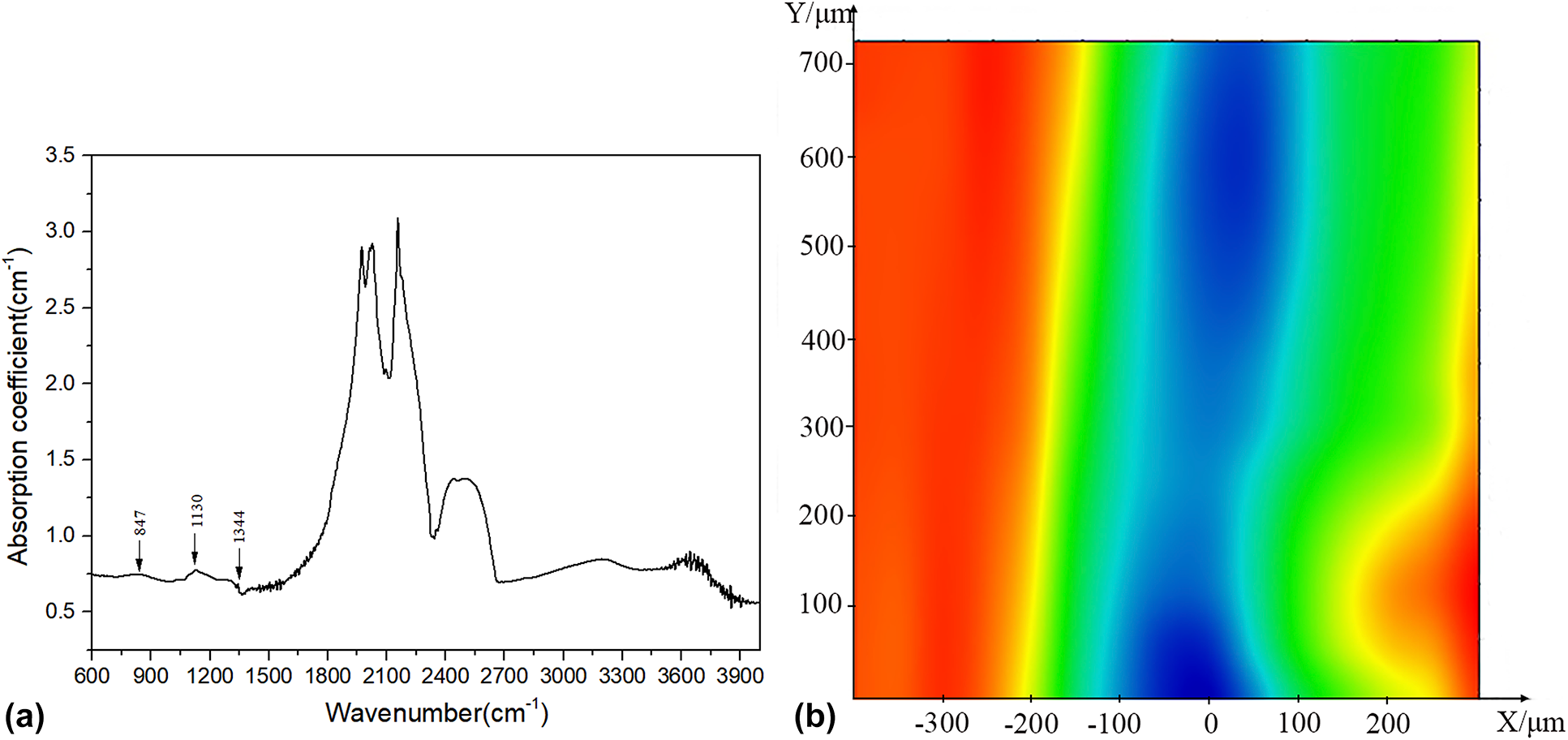
To study the interface characteristics between substrates and homoepitaxially grown single crystalline diamond layers, the high-pressure/high-temperature Ib diamond seeds with homoepitaxial diamond layers were annealed by low-pressure/high-temperature treatment in a hydrogen environment. The stress evolution and related impurity transformation near the interface were characterized by Raman spectroscopy, photoluminescence, and micro-infrared spectroscopy before and after annealing. It is found that the stress is the smallest in a 100 μm wide zone near the interface, accompanying with the similar change in substitutional nitrogen (Ns) concentration. After annealing at 1050 °C, 1250 °C, and 1450 °C, the local compressive stress is released gradually with temperature change. It is decreased by 1.03 GPa in maximum after annealing at 1450 °C. The concentration of nitrogen–vacancy (NV) complexes in the chemical vapor deposition (CVD) layer is dramatically reduced at 1450 °C. The value of ${{I_{{\rm{NV}}^ \hbox- } } \mathord{\left/ {\vphantom {{I_{{\rm{NV}}^ - } } {I_{{\rm{diamond}}} }}} \right. \kern-\nulldelimiterspace} {I_{{\rm{diamond}}} }}$ decreases much more than ${{I_{{\rm{NV}}^0 } } \mathord{\left/ {\vphantom {{I_{{\rm{NV}}^0 } } {I_{{\rm{diamond}}} }}} \right. \kern-\nulldelimiterspace} {I_{{\rm{diamond}}} }}$ in the CVD layer, which is due to the lower stability of NV compared with NV0 at high temperature.

Type
Article
Copyright
Copyright © Materials Research Society 2020

Access options

Get access to the full version of this content by using one of the access options below. (Log in options will check for institutional or personal access. Content may require purchase if you do not have access.)

Footnotes

b)

This author was an editor of this journal during the review and decision stage. For the JMR policy on review and publication of manuscripts authored by editors, please refer to http://www.mrs.org/editor-manuscripts/.

References

Kamo, M., Yurimoto, H., and Sato, Y.: Epitaxial growth of diamond on diamond substrate by plasma assisted CVD. Appl. Surf. Sci. 33, 553560 (1988).CrossRefGoogle Scholar
Shinohara, A.H., Kamo, M., and Suzuki, C.K.: A uniformly cleaved epitaxially grown diamond crystal for synchrotron radiation. J. Synchrotron Radiat. 5, 654656 (1998).CrossRefGoogle Scholar
Chu, C.J.M., D'Evelyn, P., and Hauge, R.H.: Mechanism of diamond growth chemical vapor deposition on diamond (100), (111), and (110) surfaces. J. Appl. Phys. 70, 1695 (1991).CrossRefGoogle Scholar
Sutcu, L.F., Chu, C.J., Thompson, M.S., Hauge, R.H. and Margrave, M.P.: Atomic force microscopy of (100), (110), and (111) homoepitaxial diamond films. J. Appl. Phys. 71, 59305940 (1992).CrossRefGoogle Scholar
Teraji, T., Yamamoto, T., Watanabe, K., Koide, Y., Isoya, J., Onoda, S., Ohshima, T., Rorgers, L., Jelezko, F., Neumann, P., Wrachtrup, J. and Koizumi, S.: Homoepitaxial diamond film growth: High purity, high crystalline quality, isotopic enrichment, and single color center formation. Phys. Status Solidi 212, 23652384 (2015).CrossRefGoogle Scholar
Wang, Z.Y., Dong, L.H., Wang, D.S. and Dong, Y.H.: Study of HPHT single crystal diamond as precision cutting tool material. Precis. Eng. 36, 162167 (2012).CrossRefGoogle Scholar
Ohmagari, S., Yamada, H., Tsubouchi, N., Umezawa, H., Chayahara, A., Mokuno, Y. and Takeuchi, D.: Toward high-performance diamond electronics: Control and annihilation of dislocation propagation by metal-assisted termination. Phys. Status Solidi A 216, 1900498 (2019).CrossRefGoogle Scholar
Charles, S.J., Butler, J.E., Feygelson, B.N., Newton, M.E., Corroll, D.L, Steeds, J.W., Darwish, H., Yan, C. S., Mao, H.K. and Hemley, R.J.: Characterization of nitrogen doped chemical vapor deposited single crystal diamond before and after high pressure, high temperature annealing. Phys. Status Solidi 201, 24732485 (2004).CrossRefGoogle Scholar
Kazuchits, N.M., Rusetsky, M.S., Kazuchits, V.N., Korolik, O.V., Kumar, V., Moe, K.S., Wang, W. and Zaitsev, A.M.: Comparison of HPHT and LPHT annealing of Ib synthetic diamond. Diamond Relat. Mater. 91, 156164 (2019).CrossRefGoogle Scholar
Knight, D.S. and White, W.B.: Characterization of diamond films by Raman spectroscopy. J. Mater. Res. 4, 385393 (1989).CrossRefGoogle Scholar
Ager, J.W. III and Drory, M.D.: Quantitative measurement of residual biaxial stress by Raman spectroscopy in diamond grown on a Ti alloy by chemical vapor deposition. Phys. Rev. B. 48, 2601 (1993).CrossRefGoogle ScholarPubMed
Ralchenko, V., Smolin, A., Pereverzev, V., Obraztsova, E., Korotoushenko, K., Konov, V., Lakhotkin, Y. and Loubnin, E.: Diamond deposition on steel with CVD tungsten intermediate layer. Diamond Relat. Mater. 4, 754758 (1995).CrossRefGoogle Scholar
Fischer, M., Gsell, S., Schreck, M. and Bergmaier, A.: Growth sector dependence and mechanism of stress formation in epitaxial diamond growth. Appl. Phys. Lett. 100, 041906 (2012).CrossRefGoogle Scholar
Hei, L.F., Zhao, Y., Wei, J.J., Liu, J.L., Li, C.M., Tang, W.Z. and Lu, F.X.: Interface features of the HPHT Ib substrate and homoepitaxial CVD diamond layer. Diamond Relat. Mater. 69, 3339 (2016).CrossRefGoogle Scholar
Bergman, L. and Nemanich, R.J.: Raman and photoluminescence analysis of stress state and impurity distribution in diamond thin films. J. Appl. Phys. 78, 67096719 (1995).CrossRefGoogle Scholar
Tardieu, A., Cansell, F., and Petitet, J.P.: Pressure and temperature dependence of the first-order Raman mode of diamond. J. Appl. Phys. 68, 32433245 (1990).CrossRefGoogle Scholar
Sharma, S.K., Mao, H.K., Bell, P.M. and Xu, J.A.: Measurement of stress in diamond anvils with micro-Raman spectroscopy. J. Raman Spectrosc. 16, 350352 (1985).CrossRefGoogle Scholar
Xiao, X., Sheldon, B.W., Qi, Y. and Kothari, A.K.: Intrinsic stress evolution in nanocrystalline diamond thin films with deposition temperature. Appl. Phys. Lett. 92, 131908 (2008).CrossRefGoogle Scholar
Zhang, Y., Yuan, J.H., Tan, L.M.: Effects of temperature and thickness on residual stresses of nano-diamond coating. Surf. Technol. 47, 265270 (2018).Google Scholar
Tavares, C., Koizumi, S., and Kanda, H.: Effects of RIE treatments for {111} diamond substrates on the growth of P-doped diamond thin films. Phys. Status Solidi 202, 21292133 (2005).CrossRefGoogle Scholar
Achard, J., Tallaire, A., Mille, V., Naamoun, M., Brinza, O., William, L. and Gicquel, A.: Improvement of dislocation density in thick CVD single crystal diamond films by coupling H2/O2 plasma etching and chemo-mechanical or ICP treatment of HPHT substrates. Phys. Status Solidi 211, 22642267 (2014).CrossRefGoogle Scholar
Nix, W.D. and Clemens, B.M.: Crystallite coalescence: A mechanism for intrinsic tensile stresses in thin films. J. Mater. Res. 14, 34673473 (1999).CrossRefGoogle Scholar
Steeds, J.W., Charles, S., Davis, T.J., Gilmore, A., Hayes, J., Pickard, D. and Butler, J.E.: Creation and mobility of self-interstitials in diamond by use of a transmission electron microscope and their subsequent study by photoluminescence microscopy. Diamond Relat. Mater. 8, 94100 (1999).CrossRefGoogle Scholar
Forneris, J., Tchernij, S.D., Tengattini, A., Enrico, E., Grilj, V., Skukan, N., Amato, G., Boarino, L., Jakšić, M. and Olivero, P.: Electrical control of deep NV centers in diamond by means of sub-superficial graphitic micro-electrodes. Carbon 113, 7686 (2017).CrossRefGoogle Scholar
Zaitsev, A.M.: Optical Properties of Diamond: A Data Handbook (Springer Science & Business Media, New York, 2001); pp. 228229.CrossRefGoogle Scholar
Collins, A.T.: Vacancy enhanced aggregation of nitrogen in diamond. J. Phys. C: Solid State Phys. 13, 2641 (1980).CrossRefGoogle Scholar
Goss, J.P., Briddon, P.R., Papagiannidis, S. and Jones, R.: Interstitial nitrogen and its complexes in diamond. Phys. Rev. B 70, 235208 (2004).CrossRefGoogle Scholar
Deák, P., Aradi, B., Kaviani, M., Frauenheim, T. and Gali, A.: Formation of NV centers in diamond: A theoretical study based on calculated transitions and migration of nitrogen and vacancy related defects. Phys. Rev. B 89, 075203 (2014).CrossRefGoogle Scholar
Manson, N.B. and Harrison, J.P.: Photo-ionization of the nitrogen-vacancy center in diamond. Diamond Relat. Mater. 14, 17051710 (2005).CrossRefGoogle Scholar
Meng, Y., Yan, C., Lai, J., Krasnicki, S., Shu, H., Yu, T., Liang, Q., Mao, H. and Hemley, R.J.: Enhanced optical properties of chemical vapor deposited single crystal diamond by low-pressure/high-temperature annealing. Proc. Natl. Acad. Sci. U. S. A. 105, 1762017625 (2008).CrossRefGoogle ScholarPubMed
Grazioso, F., Patton, B.R., Delaney, P., Markham, M.L., Twitchen, D.J. and Smith, J.M.: Measurement of the full stress tensor in a crystal using photoluminescence from point defects: The example of nitrogen vacancy centers in diamond. Appl. Phys. Lett. 103, 101905 (2013).CrossRefGoogle Scholar
Jin, S. and Moustakas, T.D.: Effect of nitrogen on the growth of diamond films. Appl. Phys. Lett. 65, 403405 (1994).CrossRefGoogle Scholar
Collins, A.T., Connor, A., Ly, C.H. and Shareef, A.: High-temperature annealing of optical centers in type-I diamond. J. Appl. Phys. 97, 083517 (2005).CrossRefGoogle Scholar