


Introduction
With the rapid expansion of semiconductor industry, power transistors are widely applied in the fast-growing fields such as electrical vehicles, solar energy, and giant data centers [Reference Casady and Johnson1, Reference Fujita2]. The most important figure of merit (FOM) for high frequency power transistors is R on × Q g that characterizes the energy loss for high frequency operation [Reference Zhang, Sun, Perozek, Liu, Zubair, Piedra, Chowdhury, Gao, Shepard and Palacios3, Reference Shenai4, Reference Wang, Wei, Xie, Liu, Tang and Chen5]. Here, R on is the resistance during “on” state, which is proportional to the conducting loss. Q g stands for the total gate charge, which represents the loss during switching operations. Silicon-based power devices cannot fulfill the required high FOM in high-power applications because its low breakdown electric field requires a larger gate to drain distance, which would increase the R on substantially and, thus, increase the total energy loss [Reference Chow and Tyagi6, Reference Millán, Godignon, Perpiñà, Pérez-Tomás and Rebollo7, Reference Yoder8].
Wide band gap semiconductors, including SiC, Ga2O3, and GaN, can overcome this challenge because their high breakdown electric field facilitates a smaller gate to drain distance, so that R on can be reduced proportionally. Furthermore, GaN-based high electron mobility transistors (HEMTs) can further reduce R on by introducing 2-dimensional electron gas (2DEG). However, the application of GaN-based HEMT arouses safety concerns for power electronic devices because of its intrinsically normally-on feature [Reference Östling, Ghandi and Zetterling9]. The current commercially available normally-off GaN HEMT devices are achieved by adopting the so called “cascode” configuration. This configuration consists of the series connection of a low-voltage normally-off Si-based metal oxide semiconductor field effect transistor (MOSFET) with a high voltage normally-on GaN HEMT [Reference Roccaforte, Greco, Fiorenza and Iucolano10]. Other strategies to achieve normally-off GaN HEMT, such as p-Gate [Reference Jones, Wang and Costinett11], fluorine gate [Reference Cai, Zhou, Chen and Lau12], and gate recess [Reference Saito, Takada, Kuraguchi, Tsuda and Omura13, Reference Lanford, Tanaka, Otoki and Adesida14], were proposed and received numerous attention from both academia and industry. However, their complicated fabrication process and low reliability prevent them from mass industrial-level production. Therefore, the intrinsically normally-off SiC and Ga2O3 power transistors would be more favorable in industrial applications because of their safety nature.
A key challenge for SiC and Ga2O3 devices is the lack of a suitable dielectric material that can both reduce the gate leakage and the interfacial defects [Reference Liu, Tuttle and Dhar15]. High gate leakage current would deteriorate the device reliability and increase the on-state loss. Also, interfacial defects under the gate electrode can substantially increase switching loss by trapping electrons that in turn increase Q g. Moreover, charged defects can also scatter electrons in the channel so that R on is increased as well.
SiC can form a native oxide (SiO2) with one or two order of magnitude higher interfacial defect density than the SiO2/Si interface because of the incomplete oxidation of carbon [Reference Gao, Seyller, Ley, Ciobanu, Pensl, Tadich, Riley and Leckey16, Reference Afanasev, Bassler, Pensl and Schulz17]. Moreover, the low dielectric constant (3.9) of SiO2 limits the maximum safe operating electric field, and the high breakdown field of SiC cannot be used fully [Reference Tanner, Perng, Frewin, Saddow and Chang18]. As for β-Ga2O3 transistors, Schottky gate structure [Reference Higashiwaki, Sasaki, Kuramata, Masui and Yamakoshi19, Reference Higashiwaki, Sasaki, Kuramata, Masui and Yamakoshi20] was used to form metal–semiconductor field effect transistor (MESFET). This type of structure has a nature of leaky gate that prevents high efficiency device operation and renders a low on/off ratio. HfO2 [Reference Tadjer, Mahadik, Wheeler, Glaser, Ruppalt, Koehler, Hobart, Eddy and Kub21], SiO2 [Reference Konishi, Kamimura, Wong, Sasaki, Kuramata, Yamakoshi and Higashiwaki22], and Al2O3 [Reference Carey IV, Ren, Hays, Gila, Pearton, Jang and Kuramata23, Reference Chabak, Moser, Green, Walker, Tetlak, Heller, Crespo, Fitch, McCandless and Leedy24] had been proposed as the gate dielectric to reduce the gate leakage currents. However, very few dielectric materials had been proposed to achieve a very high-quality interface along with very low leakage [Reference Higashiwaki, Sasaki, Kamimura, Hoi Wong, Krishnamurthy, Kuramata, Masui and Yamakoshi25].
Both MgO and CaO have relatively high dielectric constants (MgO 9.8, CaO 11.8) and relatively large band gaps (both 7–8 eV) compared with SiC (3.3 eV) and Ga2O3 (4.5–4.9 eV) and, thus, might be suitable gate oxides for wide band gap semiconductors. Recently, our group has demonstrated that an epitaxial MgxCa1−xO film can be grown on GaN(0001) surfaces using a suitable ALD process, achieving low interfacial defect density and high electrical performance [Reference Lou, Zhou, Kim, Alghamdi, Gong, Feng, Wang, Ye and Gordon26]. We demonstrated a low defect density interface between semiconductor substrates and a lattice matched epitaxial gate dielectric material. Q g can be effectively minimized with this reduced interfacial defect density, and therefore, the overall device loss was reduced. Moreover, because there are few grain boundaries to serve as the leakage pathways, gate leakage loss was also reduced. 4H SiC has a similar hexagonal symmetry on the (0001) surface with the GaN(0001). With only −4% of lattice mismatch with GaN, SiC is widely used as the epitaxial growth substrate for GaN in LED industry. Bhuiyan et al. also demonstrated that MgxCa1−xO is a promising radiation-tolerant gate dielectric material for GaN-based MOSHEMTs [Reference Bhuiyan, Zhou, Chang, Lou, Gong, Jiang, Gong, Zhang, Won and Lim27]. β-Ga2O3 on the other hand has a monolithic structure that does not exactly match the hexagonal symmetry of the rock salt MgxCa1−xO(111) surface. But its  $\left( {\bar 201} \right)$ surface has a structure similar to a hexagonal structure, which makes it also suitable as the substrate for GaN epitaxial growth [Reference Tsai, Horng, Wuu, Ou, Hung and Hsueh28, Reference Víllora, Shimamura, Kitamura, Aoki and Ujiie29]. Therefore, it is highly possible to grow MgxCa1−xO epitaxially on the SiC(0001) and β-Ga2O3 $\left( {\bar 201} \right)$ surfaces which are close to GaN(0001).
Moreover, as shown in Fig. 1, the SiC lattice sizes lie between those of MgO and CaO lattices. Therefore, by tuning the composition of MgxCa1−xO, a lattice match with SiC substrates can be achieved. According to Vegard’s Law [Reference Morkoç30], a 76% Mg and 24% Ca oxide mixture can achieve a lattice match with SiC with an epitaxy relation of  $\left( {111} \right)_{{\rm{Mg}}_{\it x} {\rm{Ca}}_{1 - {\it x}} {\rm{O}}} //\left( {0001} \right)_{{\rm{SiC}}}$. In the meantime, because β-Ga2O3 $\left( {\bar 201} \right)$ surface is similar to GaN(0001) surface, it is anticipated to be latticed match with a composition near Mg0.25Ca0.75O. Epitaxial Mg0.75Ca0.25O grown by molecular beam epitaxy (MBE) on SiC has been reported as an alternative dielectric oxide [Reference Stodilka, Gerger, Hlad, Kumar, Gila, Singh, Abernathy, Pearton and Ren31]. Moreover, epitaxial GaN has been reported to be grown on β-Ga2O3 $\left( {\bar 201} \right)$ surface by MBE [Reference Ohira, Suzuki, Minami, Takahashi, Araki and Nanishi32]. Therefore, MBE-grown dielectrics can be expected for Ga2O3 substrates as well. Measurements on HEMTs with MBE-fabricated MgCaO insulators showed improved gate-lag [Reference Gila, Hlad, Onstine, Frazier, Thaler, Herrero, Lambers, Abernathy, Pearton and Anderson33]. However, MBE endures problems such as low industrial compatibility due to ultra-high vacuum requirements and high cost. Furthermore, MBE is not applicable to large substrates needed for cost-effective industrial processing. Thus, a more scalable and lower cost method to deposit epitaxial MgxCa1−xO is highly desirable. Atomic layer deposition (ALD) is a well-established method to achieve films with high uniformity and highly controllable precision. Moreover, ALD technique is more cost effective and industrial compatible compared with MBE, providing potential way to achieve precisely controlled and high-quality dielectric films. Thus, in this study, we focused on applying the ALD process to grow epitaxially MgxCa1−xO on SiC(0001) and β-Ga2O3 $\left( {\bar 201} \right)$ substrates.

Figure 1: (a) 2θ–ω scans of three MgxCa1−xO/SiC samples. (b) Lattice constant of MgxCa1−xO with respect to Ca content in the film. Comparing SiC(0004) lattice with MgxCa1−xO(222) lattice, it shows that the Mg0.72Ca0.28O has the smallest lattice mismatch with SiC.
Results and discussions
Epitaxial growth of MgxCa1−xO on SiC
SiC has two primary polytypes for semiconductor applications, 4H and 6H, respectively. Both 4H and 6H are hexagonal, and each has a similar (0001) surface structure and a relatively small lattice mismatch to GaN, −3.8% and −3.5%, respectively. Traditionally, 4–8 degrees of off-axis SiC were grown with liquid or vapor phase epitaxial growth because the higher density of surface steps can improve the growth quality [Reference Ueda, Nishino and Matsunami34]. However, Hijikata et al. had pointed out that the lower angle of off-axis SiC can effectively reduce the interfacial traps [Reference Hijikata, Yaguchi, Yoshida, Takata, Kobayashi, Nohira and Hattori35]. In our case, the surface symmetry of off-angle SiC also does not match with the hexagonal structure of rock salt (111) surface. Therefore, an on-axis SiC 4H is selected as the substrate. To perform a comprehensive study on how lattice mismatch influences epitaxy growth, films with three compositions such as pure MgO, Mg0.72Ca0.28O, and Mg0.51Ca0.49O were investigated. According to Vegard’s law, as shown in Fig. 1(b), the SiC lattice matches with Mg0.72Ca0.28O is expected to have best epitaxy quality. The substrate surface pretreatments and ALD MgxCa1−xO deposition were performed with the conditions described in the Experiments and Methods section. X-ray diffraction (XRD) was conducted to further confirm the lattice matching of the MgxCa1−xO and SiC substrate. Figure 1(a) shows 2θ–ω scans of three MgxCa1−xO/SiC samples. 2θ–ω results show that the lattice mismatch of Mg0.51Ca0.49O and Mg0.72Ca0.28O are +3.2% and +0.7%, and −3.9%, respectively. It is clear that the Mg0.72Ca0.28O has the closest match with SiC. This result is further verified by the corresponding rocking curves shown in Fig. 2. The narrower rocking curve of Mg0.72Ca0.28O/SiC (FWHM = 0.1°) than Mg0.51Ca0.49O/SiC (FWHM = 0.36°) and MgO/SiC (FWHM = 0.39°) indicates the former has the highest epitaxial quality. The fact that the lattice constants of MgxCa1−xO films are very close to the corresponding Vegard’s law prediction, indicating that there is little stress. The extra sharpness of the Mg0.51Ca0.49O and Mg0.72Ca0.28O’s rocking curve might be due to the relaxation of the top layer of the film.

Figure 2: Rocking curves of MgxCa1−xO/4H-SiC(0001). (a) Rocking curve of Mg0.51Ca0.49O/SiC at 2θ = 72.55°. (b) Rocking curve of Mg0.72Ca0.28O/SiC at 2θ = 74.70°. (c) Rocking curve of MgO/SiC at 2θ = 78.96°.
Ren et al. had pointed out that the drawback of this ternary dielectric system is the large difference in the ionic radius between Mg and Ca causing severe immiscibility [Reference Stodilka, Gerger, Hlad, Kumar, Gila, Singh, Abernathy, Pearton and Ren31, Reference Doman, Barr and McNally36], particularly at high temperature. As a result, solid-solution CaO–MgO would be difficult to synthesize using bulk techniques because the two phases are immiscible over the entire composition range. However, the use of ALD as a film growth technique often allows for the formation of metastable phases, overcoming miscibility issues due to the unique self-terminating nature of growth. According to our research, MgxCa1−xO ternaries are kinetically stable as solid solution films over the entire compositional range when grown at a remarkably low temperature of 300 °C. The absence of CaO and MgO peaks in the XRD pattern also confirmed that there is no phase separation.
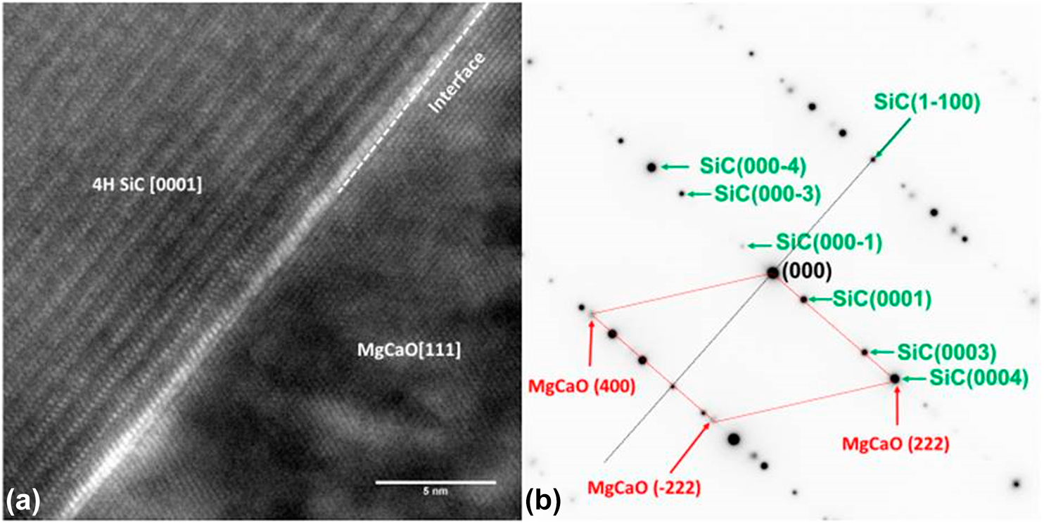
Cross-sectional transmission electron microscopy (TEM) was used to study the interfacial region of this epitaxial structure. Like the typical GaN cross-sectional TEM, SiC also shows a three atomic line periodicity pattern in the vertical direction because of its hexagonal structure [Reference Lou, Zhou, Kim, Alghamdi, Gong, Feng, Wang, Ye and Gordon26]. Therefore, the interface between the substrate and MgxCa1−xO film can be determined by where this three-line periodicity discontinued. A sharp interface without any interfacial layer can be seen in Figs. 3(a) and 3(c). The traditional oxidized SiO2 dielectric on SiC is caused by the roughened interface [Reference Hosoi, Konzono, Uenishi, Mitani, Nakano, Nakamura, Shimura and Watanabe37]. In the ALD-grown epitaxial MgxCa1−xO on SiC, the pristine interface is preserved. The very well-defined diffraction spots in (b) also confirm the high epitaxial quality of the film. Twinning formation is common in crystalline films, with 180° mirror images having almost identical formation energy as shown in the Mg0.72Ca0.28O left-right symmetric diffraction pattern [Reference Sridhar, Rickman and Srolovitz38, Reference Tanner, Toney, Lu, Blom, Sawkar-Mathur, Tafesse and Chang39]. Moreover, from the diffraction pattern, the zone axis of the SiC substrate in these TEM images is  $\left[ {11\bar 20} \right]$, and the film zone axis can be determined as $\left[ {0\bar 11} \right]$. Therefore, the epitaxial relation between the film and substrate is Mg0.72Ca0.28O(111) × $\left[ {0\bar 11} \right]$//SiC(0001) × $\left[ {11\bar 20} \right]$. Theoretical studies on MgxCa1−xO ternary systems also predicted a CsCl phase is possible [Reference Srivastava, Chauhan, Singh and Padegaonker40]. But the TEM diffraction pattern clearly showed that there is no phase other than rock salt and also no phase separation is observed.

Figure 3: TEM cross section of Mg0.72Ca0.28O/SiC(0001). (a) Cross-sectional TEM image. (b) Diffraction pattern of the (a) region. The zone axis of the SiC is  $\left[ {11\bar 20} \right]$ and for Mg0.72Ca0.28O is $\left[ {0\bar 11} \right]$.
In summary, the XRD and TEM studies confirmed that the ALD MgxCa1−xO can be grown epitaxially on 4H-SiC (0001) substrates. Mg0.72Ca0.28O shows the best lattice match with a +0.7% mismatch with the SiC substrate. The rocking curve also confirms that this smaller lattice match has a better epitaxial quality than the samples with larger mismatch.
Epitaxial growth of MgxCa1−xO on Ga2O3
Although β-Ga2O3 has a monoclinic crystal structure and does not have hexagonal symmetry on any crystal face, the O atoms on β-Ga2O3 $\left( {\bar 201} \right)$ surface are roughly lined up on the same plane [Fig. 4(a)] and formed a nearly hexagonal structure from the top view [Fig. 4(b)]. Moreover, the distance between these O atoms are close to the distance between the N atoms on GaN(0001). Kitamura et al. had demonstrated that an epitaxial GaN can be grown on β-Ga2O3, with a lattice mismatch as small as 2.6%. Therefore, it is possible to create an epitaxial growth of MgxCa1−xO on a β-Ga2O3 $\left( {\bar 201} \right)$ surface as shown in Fig. 4.

Figure 4: (a) Side view of β-Ga2O3 $\left( {\bar 201} \right)$ lattice. (b) Top view of MgxCa1−xO(111)/β-Ga2O3 $\left( {\bar 201} \right)$.
As shown in Fig. 4(b), there are also two different possible orientations denoted as A and B. In both cases, Mg/Ca atoms are always stacking over substrate O atoms. In case A, half of film oxygen atoms are stacking over Ga atoms and the other half are on the vacancies surrounded by three oxygen atoms from the substrate. On the other hand, in case B, the film oxygen atoms are all on top of the vacancies surrounded by three oxygen atoms from the substrate. Thus, a φ scan is used to determine which orientation is achieved with ALD growth. The MgxCa1−xO(200) peak and Ga2O3(202) peak are close in both 2θ and ω offset in MgxCa1−xO(111)/β-Ga2O3 $\left( {\bar 201} \right)$ structure. Therefore, a φ scan is set for scanning based on the position of Ga2O3(202) peak at ψ 54° and 2θ 38.62°. Figure 5 demonstrates the φ scan of Mg0.25Ca0.75O/β-Ga2O3, which has a 3-fold symmetry, confirming that there is only one in-plane orientation existing in the film. Furthermore, the substrate (202) peak does not overlap with the film (200) peaks in φ scan, indicating that the film has a B-type orientation as shown in previously in Fig. 4(b).

Figure 5: φ scan of Mg0.25Ca0.75O/Ga2O3 $\left( {\bar 201} \right)$.
To achieve epitaxial growth of MgxCa1−xO on β-Ga2O3 substrates, ultra-clean surfaces of β-Ga2O3 substrate are needed. However, β-Ga2O3 is unstable under both acidic and basic conditions. Therefore, its surface treatment is very challenging. Some reports show that Piranha and buffered oxide etch (BOE) treatments are effective to prepare the β-Ga2O3 surface [Reference Yang, Sparks, Ren, Pearton and Tadjer41]. In this study, both pretreatments are used for comparison.
The cross-sectional TEM images of Mg0.25Ca0.75O grown on both Piranha and BOE treated β-Ga2O3 $\left( {\bar 201} \right)$ are shown in Figs. 6 and 7, respectively. The Piranha treatment is a common method for β-Ga2O3 surface cleaning used in a few Refs. [Reference Jayawardena, Ahyi and Dhar42, Reference Zhou, Si, Alghamdi, Qiu, Yang and Peide43]. Although benefiting electrical performance in the literature, the Piranha-treated sample exhibits a 10 nm amorphous-like interfacial layer. This interfacial layer may be from the hydroxylation of β-Ga2O3 in the acid pretreatment.

Figure 6: Cross-sectional TEM of (a) Piranha-treated bare Ga2O3 surface and (b) Mg0.25Ca0.75O on Piranha-treated Ga2O3.

Figure 7: TEM of Mg0.25Ca0.75O/Ga2O3 $\left( {\bar 201} \right)$ after BOE surface treatment. (a) High resolution image of Mg0.25Ca0.75O and Ga2O3 interface, a 2 nm interfacial layer is visible. (b) Diffraction pattern. The zone axis of β-Ga2O3 is [010]. The main diffraction spots of Mg0.25Ca0.75O indicate that the zone axis of the film is $\left[ {0\bar 11} \right]$. The stray diffraction spots from Mg0.25Ca0.75O are indicating that the film is highly textured with some misoriented crystal phases.
In the meantime, as shown in Fig. 7(a), the 30 s BOE-treated sample (1:6 original diluted with 5 times volume of water) has only a 2 nm interfacial layer. This is a substantial improvement compared with the Piranha-treated substrate. However, severe delamination has been observed on the edge of β-Ga2O3 substrates, indicating surface damage caused by BOE treatment. In Fig. 7(b), the diffraction pattern of both the film and substrate indicates an epitaxial relationship to be MgxCa1−xO $\left[ {0\bar 11} \right]$ × (111)//β-Ga2O3 $[010]$ × $\left( {\bar 201} \right)$. In addition, the diffraction pattern in Fig. 7(b) indicates a highly textured film, with some misoriented crystal phases.
XRD was then carried out to further investigate the epitaxial growth quality of Mg0.25Ca0.75O/β-Ga2O3. The full 2θ–ω scan of Mg0.25Ca0.75O/β-Ga2O3 is demonstrated in Fig. 8. The existence of (111) and (222) peaks of Mg0.25Ca0.75O indicates the film has a preferred (111) orientation. The (222) peak of the film is not as obvious as (111) because it is overlapping with (801) peak from the substrate. The β-Ga2O3(111), (601), and (801) peaks indicate that the substrate contains other small crystals with disordered orientations.

Figure 8: 2θ–ω of Mg0.25Ca0.75O/Ga2O3 and bare Ga2O3.
In summary, highly textured Mg0.25Ca0.75O can be grown on β-Ga2O3 $\left( {\bar 201} \right)$ with a preferred orientation of (111). The dielectric films are highly textured rather than epitaxial mainly because β-Ga2O3 $\left( {\bar 201} \right)$ lattice is not perfectly hexagonal, which can introduce mismatch to the film (111) surface. Another minor cause might be the nonideal surface pretreatments. The β-Ga2O3 surface pretreatment has a profound effect on the interfacial property. BOE treatment can effectively reduce the interfacial layer thickness damages of the substrate to some extent.
Conclusion
In this work, we demonstrated for the first time that epitaxial and highly textured MgxCa1−xO can be grown on SiC(0001) and β-Ga2O3 $\left( {\bar 201} \right)$ with an ALD process. Because SiC(0001) has hexagonal symmetry, MgxCa1−xO can be grown epitaxially on it. The closest lattice matching Mg0.72Ca0.28O showed the highest epitaxy quality in an XRD rocking scan. Therefore, it has the greatest potential to achieve superior dielectric properties and should be the best candidate for device applications. In the meantime, highly textured Mg0.25Ca0.75O can be grown on β-Ga2O3 $\left( {\bar 201} \right)$ with a preferred orientation of (111). The Mg0.25Ca0.75O film on β-Ga2O3 $\left( {\bar 201} \right)$ is textured instead of epitaxial because the substrate surface is not perfectly matching the hexagonal symmetry of the film (111) surface. The crystal orientation relationship between MgxCa1−xO and β-Ga2O3 was determined by XRD scans. Cross-sectional TEM showed that BOE treatment can effectively reduce the thickness of amorphous β-Ga2O3 top layer compared with Piranha treatment.
Experiments and methods
Substrate pretreatments
Both SiC and Ga2O3 substrates were purchased from MTI Corp. Surface pretreatments of substrates are crucial to the success of epitaxial growth of MgxCa1−xO films because epitaxy is very sensitive to interfacial conditions. SiC substrates were soaked and rinsed 5 min in isopropanol and acetone and then methanol was conducted subsequently as basic surface cleaning. Then a 5 min UV-ozone and 30 s buffered oxide etch (BOE; 1:6 original diluted with 5 times volume water) were followed to remove the organic contaminants and surface oxide. In the case of Ga2O3, same surface pretreatment procedures were carried out for one batch of substrates. As a comparison experiment, the final step of 30 s BOE etch was replaced with 30 s Piranha (a mixture of 3:1 sulfuric acid and hydrogen peroxide) etch for the other batch of substrates.
MgxCa1−xO film growth
ALD of MgxCa1−xO was carried out in a home-built tubular reactor. MgxCa1−xO films were obtained by alternating doses of calcium, magnesium, and oxygen sources, where bis(N,N′-diisopropylacetamidinato)calcium(II) dimer [Reference Saito, Takada, Kuraguchi, Tsuda and Omura13], bis(N,N′-di-sec-butylacetamidinato)magnesium, and H2O were used as precursors, respectively. Structural formulas for Mg and Ca precursors are shown in Fig. 9. The Mg precursor is kept at 110 °C, whereas the Ca precursor is kept at 140 °C to provide enough vapor pressure. H2O is kept at room temperature. During the deposition, the samples/substrates are placed on the substrate holder kept at 310 °C under vacuum. In each dosing cycle, either the Mg or Ca precursor is dosed into the reaction chamber and then purged for 30 s. Then H2O vapor is dosed and purged. Four different precursor dosing ratios, namely, Mg only, Mg:Ca = 1:1, Mg:Ca = 1:2, and Mg:Ca = 1:3, were used. The dosing sequence is repeated for the corresponding number of Mg cycles, then Ca cycles. Because of the large size of the ligands, each metal cycle cannot fully cover one atomic layer. Therefore, the alternating Mg and Ca cycles can give a uniform film instead of layered structure. The compositions of the resulting films were determined by RBS (Rutherford Backscattering Spectrometry) to be MgO, Mg0.72Ca0.28O, Mg0.51Ca0.49O, and Mg0.25Ca0.75O, respectively. The film growth rates with different dosing ratios and the corresponding compositions are summarized in the literature published by our group [Reference Lou, Zhou, Kim, Alghamdi, Gong, Feng, Wang, Ye and Gordon26]. The total ALD MgxCa1−xO film thickness is 40 nm for further characterization. Because MgO and CaO are both reactive with moisture, a 5 nm of Al2O3 is grown in situ on top of MgxCa1−xO for both SiC and β-Ga2O3 substrates to prevent water in air from permeation into the epitaxial film during XRD and TEM characterization.

Figure 9: Structures of the metal precursors. (a) bis(N,N′-di-sec-butylacetamidinato)magnesium and (b) bis(N,N′-diisopropylacetamidinato)calcium(II) dimer.
Film epitaxy characterizations
Cross-sectional TEM and diffraction patterns were conducted on MgxCa1−xO/SiC and MgxCa1−xO/Ga2O3 samples with the Joel 2100 High resolution TEM in Harvard CNS (Center for Nanoscale Systems). The TEM samples were beforehand prepared with an FEI Helios 660 FIB (focused ion beam) system and then cleaned with 500 eV Ar ion beam with a Fischione NanoMill 1040 in Harvard CNS. XRD measurements were carried out in the Bruker D8 high resolution XRD facility in Harvard CCB (Chemistry & Chemical Biology Department) X-ray Laboratory. The φ scan of MgxCa1−xO is achieved by first determining the 2θ and ω angle of MgxCa1−xO (200) position with asymmetric 2θ–ω scan and rocking scan. Then a φ scan is conducted by collecting the MgxCa1−xO (200) peak while rotating the sample stage.
Author contributions
The manuscript was written through contributions of all authors. X.B.L. and X.G. contributed equally.
Supplementary material
To view supplementary material for this article, please visit https://doi.org/10.1557/jmr.2019.376.
Acknowledgments
This work was supported by the US National Science Foundation grant 1764338, the US Office of Naval Research contract N00014-10-1-0937, the US Department of Energy—Office of Science contract DE-AC36-08GO28308, and the Charles Stark Draper Laboratory, Inc. contract SC001-0000000950. This work was performed in part at the Harvard University Center for Nanoscale Systems (CNS), a member of the National Nanotechnology Coordinated Infrastructure Network (NNCI), which is supported by the National Science Foundation under NSF ECCS Award No. 1541959.


