Hostname: page-component-848d4c4894-nr4z6 Total loading time: 0 Render date: 2024-05-09T23:42:47.825Z Has data issue: false hasContentIssue false

Improved ultraviolet sensing, photo-stabilized visible transmission, and electrical conductance in Zn1−xGax/2Fex/2O

Published online by Cambridge University Press:  19 May 2020

Prashant Kumar Mishra
Affiliation:
Discipline of Physics, Indian Institute of Technology, Indore 453552, India
Aditya Dash
Affiliation:
Department of Physics and Astronomy, National Institute of Technology Rourkela, Odisha 769008, India
Somaditya Sen*
Affiliation:
Department of Electronic Engineering and Organic Electronics Research Center, Ming Chi University of Technology, New Taipei City 243, Taiwan
*
a)Address all correspondence to this author. e-mail: sens@iiti.ac.in
Get access

Abstract

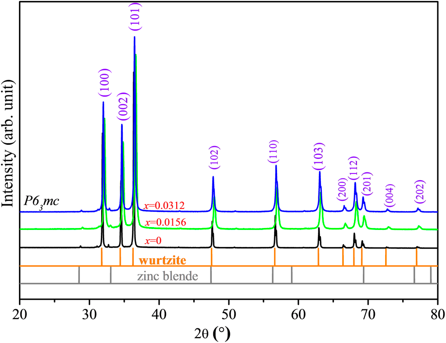
Zn1−xGax/2Fex/2O (x= 0, 0.0156, 0.0312) represents the polycrystalline hexagonal (wurtzite) phase with a space group P63mc synthesized using the sol–gel technique. A comparative study and investigation of structural, optical, and photo-sensing properties of these samples were performed. Structural and vibrational studies show enhancement in the crystallinity of the codoped samples. Optical band gap increases from 3.21 to 3.24 eV with substitution because of the improved crystallinity. The photoluminescence properties show modification from yellowish green for x= 0 to a more distinct green for x= 0.0156. The intensity of the luminescence decreases with doping, indicating an overall reduction of defects in the band gap helping the material to become more transparent to visible light. Photocurrent and photosensitivity are modified with the illumination wavelength (290, 450, 540 and 640 nm) with codoping. Sensitivity toward visible lights reduced with codoping. On the other hand, it is more sensitive to ultraviolet light. It indicates the material becomes more transparent for visible light and may be used as photostable device.

Type
Article
Copyright
Copyright © Materials Research Society 2020

Access options

Get access to the full version of this content by using one of the access options below. (Log in options will check for institutional or personal access. Content may require purchase if you do not have access.)

References

Akay, S.K., Sarsıcı, S., and Kaplan, H.K.: Determination of electrical parameters of ZnO/Si heterojunction device fabricated by RF magnetron sputtering. Opt. Quant. Electron. 50, 362 (2018).CrossRefGoogle Scholar
Agarwal, D.C., Singh, U.B., Gupta, S., Singhal, R., Kulriya, P.K., Singh, F., Tripathi, A., Singh, J., Joshi, U.S., and Avasthi, D.K.: Enhanced room temperature ferromagnetism and green photoluminescence in Cu doped ZnO thin film synthesised by neutral beam sputtering. Sci. Rep. 9, 1 (2019).CrossRefGoogle ScholarPubMed
Ali, G.M. and Chakrabarti, P.: Performance of ZnO-based ultraviolet photodetectors under varying thermal treatment. IEEE Photonics J. 2, 784 (2010).CrossRefGoogle Scholar
Alagha, S., Heedt, S., Vakulov, D., Mohammadbeigi, F., Kumar, E.S., Schäpers, T., Isheim, D., Watkins, S.P., and Kavanagh, K.L.: Electrical properties of lightly Ga-doped ZnO nanowires. Semicond. Sci. Technol. 32, 125010 (2017).CrossRefGoogle Scholar
Singh, J., Ranwa, S., Akhtar, J., and Kumar, M.: Growth of residual stress-free ZnO films on SiO2/Si substrate at room temperature for MEMS devices. AIP Adv. 5, 067140 (2015).CrossRefGoogle Scholar
Fan, S-W., Srivastava, A.K., and Dravid, V.P.: UV-activated room-temperature gas sensing mechanism of polycrystalline ZnO. Appl. Phys. Lett. 95, 142106 (2009).CrossRefGoogle Scholar
Hullavarad, S., Hullavarad, N., Look, D., and Claflin, B.: Persistent photoconductivity studies in nanostructured ZnO UV sensors. Nanoscale Res. Lett. 4, 1421 (2009).CrossRefGoogle ScholarPubMed
Chen, C-Y., Hsiao, L-H., and Chyi, J-I.: Influence of point defects on the properties of undoped and Ga-doped ZnO films grown by plasma-assisted molecular beam epitaxy in an O-rich environment. ECS J. Solid State Sci. Technol. 5, Q222 (2016).CrossRefGoogle Scholar
Barbagiovanni, E.G., Strano, V., Franzò, G., Crupi, I., and Mirabella, S.: Photoluminescence transient study of surface defects in ZnO nanorods grown by chemical bath deposition. Appl. Phys. Lett. 106, 093108 (2015).CrossRefGoogle Scholar
Ayaz, S., Mishra, P., and Sen, S.: Structure correlated optoelectronic and electrochemical properties of Al/Li modified ZnO. J. Appl. Phys. 126, 024302 (2019).CrossRefGoogle Scholar
Harun, K., Hussain, F., Purwanto, A., Sahraoui, B., Zawadzka, A., and Mohamad, A.A.: Sol–gel synthesized ZnO for optoelectronics applications: A characterization review. Mater. Res. Express 4, 122001 (2017).CrossRefGoogle Scholar
Lin, C., Chang, S-J., Chen, W-S., and Hsueh, T-J.: Transparent ZnO-nanowire-based device for UV light detection and ethanol gas sensing on c-Si solar cell. RSC Adv. 6, 11146 (2016).CrossRefGoogle Scholar
Schmidt-Mende, L. and MacManus-Driscoll, J.L.: ZnO nanostructures, defects, and devices. Mater. Today 10, 40 (2007).CrossRefGoogle Scholar
Srivastava, T., Bajpai, G., Rathore, G., Liu, S.W., Biring, S., and Sen, S.: Vanadium substitution: A simple and economic way to improve UV sensing in ZnO. J. Appl. Phys. 123, 161407 (2018).CrossRefGoogle Scholar
Gimenez, A.J., Yáñez-Limón, J.M., and Seminario, J.M.: ZnO paper based photoconductive UV sensor. J. Phys. Chem. C 115, 282 (2011).CrossRefGoogle Scholar
Bajpai, G., Srivastava, T., Patra, N., Moirangthem, I., Jha, S.N., Bhattacharyya, D., Riyajuddin, S., Ghosh, K., Basaula, D.R., Khan, M., Liu, S-W., Biring, S., and Sen, S.: Effect of ionic size compensation by Ag+ incorporation in homogeneous Fe-substituted ZnO: Studies on structural, mechanical, optical, and magnetic properties. RSC Adv. 8, 24355 (2018).CrossRefGoogle Scholar
Pat, S., Mohammadigharehbagh, R., Musaoglu, C., Özen, S., and Korkmaz, Ş.: Investigation of the surface, morphological and optical properties of boron-doped ZnO thin films deposited by thermionic vacuum arc technique. Mater. Res. Express 5, 066419 (2018).CrossRefGoogle Scholar
Das, J., Mishra, D.K., Srinivasu, V.V., Sahu, D.R., and Roul, B.K.: Photoluminescence and Raman studies for the confirmation of oxygen vacancies to induce ferromagnetism in Fe doped Mn:ZnO compound. J. Magn. Magn. Mater. 382, 111 (2015).CrossRefGoogle Scholar
Fukushima, H., Uchida, H., Funakubo, H., Katoda, T., and Nishida, K.: Evaluation of oxygen vacancies in ZnO single crystals and powders by micro-Raman spectroscopy. J. Ceram. Soc. Jpn. 125, 445 (2017).CrossRefGoogle Scholar
Kirste, R., Aksu, Y., Wagner, M.R., Khachadorian, S., Jana, S., Driess, M., Thomsen, C., and Hoffmann, A.: Raman and photoluminescence spectroscopic detection of surface-bound Li+O2 defect sites in Li-doped ZnO nanocrystals derived from molecular precursors. Chemphyschem 12, 1189 (2011).CrossRefGoogle ScholarPubMed
Korepanov, V.I., Chan, S-Y., Hsu, H-C., and Hamaguchi, H.: Phonon confinement and size effect in Raman spectra of ZnO nanoparticles. Heliyon 5, e01222 (2019).CrossRefGoogle ScholarPubMed
Srivastava, T., Rini, E.G., Joshi, A., Shirage, P., and Sen, S.: Zn1−xSixO: Improved optical transmission and electrical conductivity. Ceram. Int. 43, 56685673, (2017).CrossRefGoogle Scholar
Rai, R.C.: Analysis of the Urbach tails in absorption spectra of undoped ZnO thin films. J. Appl. Phys. 113, 153508 (2013).CrossRefGoogle Scholar
Dimova‐Malinovska, D., Nichev, H., and Angelov, O.: Correlation between the stress in ZnO thin films and the Urbach band tail width. Phys. Status Solidi C 5, 3353 (2008).CrossRefGoogle Scholar
Barbagiovanni, E.G., Reitano, R., Franzò, G., Strano, V., Terrasi, A., and Mirabella, S.: Radiative mechanism and surface modification of four visible deep level defect states in ZnO nanorods. Nanoscale 8, 995 (2015).CrossRefGoogle Scholar
Chen, H., Ding, J., Guo, W., Chen, G., and Ma, S.: Blue-green emission mechanism and spectral shift of Al-doped ZnO films related to defect levels. RSC Adv. 3, 12327 (2013).CrossRefGoogle Scholar
Granerød, C.S., Bilden, S.R., Aarholt, T., Yao, Y-F., Yang, C.C., Look, D.C., Vines, L., Johansen, K.M., and Prytz, Ø.: Direct observation of conduction band plasmons and the related burstein-moss shift in highly doped semiconductors: A STEM-EELS study of Ga-doped ZnO. Phys. Rev. B 98, 115301 (2018).CrossRefGoogle Scholar
Supplementary material: File

Mishra et al. Supplementary Materials

Mishra et al. Supplementary Materials

Download Mishra et al. Supplementary Materials(File)
File 968.7 KB