


I. INTRODUCTION
Mesoscale science and engineering, broadly defined as the study and application of materials systems bridging the quantum and continuum regimes, is an area rich with new paradigms and research topics. 1–Reference Yip and Short3 One area of interest falling under this general classification is the understanding and control of dynamic responses of defect-laden structures and systems. At spatial scales exceeding those of individual atoms and nanometer-scale assemblies, defects become increasingly prevalent. Consequently, the emergent properties of the system are increasingly influenced and dictated by heterogeneously-distributed particles, defects, and interfaces, as evinced in mechanical, electronic, and magnetic behaviors. Reference Kalinin and Spaldin4–Reference Hoffmann and Schultheiß6 Fine control of materials properties then becomes possible through the rational design of such mesoscale structures and materials, the fundamental understanding of which can be informed by direct characterization with multimodal (ideally all-in-one) instrumentation that can cover a wide range of spatial and temporal scales. 1
A still-emerging laboratory-scale characterization modality that is well-suited for conducting mesoscale studies is ultrafast electron microscopy (UEM). Reference Zewail7,Reference Piazza, Masiel, LaGrange, Reed, Barwick and Carbone8 With UEM, structural, electronic, and temporal information can be gathered with a single, properly-equipped instrument, with the multidimensional experimentally accessible parameter space spanning many orders of magnitude. Reference Flannigan and Zewail9 Indeed, stroboscopic UEM can be used to access timescales ranging from the limits of current state-of-the-art detector technology (approximately milliseconds) down to femtoseconds. Importantly, the ease with which electron trajectories can be manipulated with magnetic and electrostatic lenses enables rapid access to both real- and reciprocal-space information, in the same way as is done with a conventional transmission electron microscope (TEM). Reference Plemmons, Suri and Flannigan10 This capability is useful for studying the effects of heterogeneously distributed defects on a variety of response and transport phenomena and for circumventing challenges associated with statistical averaging. Reference van der Veen, Kwon, Tissot, Hauser and Zewail11,Reference Cremons, Plemmons and Flannigan12
Here, we demonstrate the multimodal capabilities of UEM by visualizing the MHz linear elastic optomechanical response of a single-crystal Si cantilever from atomic to micrometer length scales. The use of Si in a wide range of electronic and mechanical applications stems from its low cost, ease of processability, and favorable structural and electronic properties. Reference Khang, Jiang, Huang and Rogers13–Reference Kim, Ahn, Choi, Kim, Kim, Song, Huang, Liu, Lu and Rogers15 In addition, despite being a thoroughly-studied material, new insights into various constitutive relations (e.g., thermal transport, linear-elastic response, etc.) continue to be found. Reference Boyd and Uttamchandani16–Reference Hu, Zeng, Minnich, Dresselhaus and Chen18 Previous reciprocal-space UEM studies on single-crystal Si wedges have resolved shear-wave motion and ultrafast vibrational responses induced by coherent photoexcitation. Reference Yurtsever and Zewail19–Reference Yurtsever, Schaefer and Zewail21 As we will demonstrate here, a multimodal approach—combining real- and reciprocal-space information—enables spatial localization of photoinduced vibrational eigenmodes, opening the way to resolving the effects of nanoscale heterogeneity on statistical variability and fluctuations.
II. MATERIALS AND METHODS
A. Specimen preparation
The Si-wedge specimen was fabricated from a 〈011〉 flat, undoped wafer (Virginia Semiconductor). Thinning was accomplished using a rigorous mechanical-polishing procedure. Reference Voyles, Grazul and Muller22 The wedge was then epoxy bonded to a copper slot grid and ion milled with a precision ion polishing system (Gatan) to electron transparency. In addition to dislocations and impurities, fractures at the edge of the specimen, which occurred during polishing and subsequent handling, produced nonsymmetric boundary conditions at the edge of the cantilever. Figure 1 displays an overview of the specimen morphology within the region of interest studied here.
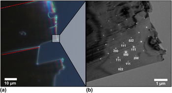
FIG. 1. Structural morphology and atomic order of the Si cantilever 2°-wedge specimen. (a) Optical dark-field image of the overall region of interest. The wedge is a cantilever; it is fixed at one end (the thick end) and free on the other sides, akin to a diving board. Note the interference fringes present at the free edge. The red dashed lines outline the region dimensions that yield the observed vibrational frequencies (discussed below). The black box denotes the specific area studied with UEM. (b) Overlay of a bright-field (BF) UEM image and properly-oriented parallel-beam diffraction pattern, as viewed along the [011] zone axis at the approximate center of the region of interest. Several Bragg spots are indexed for reference.
B. Ultrafast electron microscopy
The optomechanical response of the Si wedge specimen to femtosecond (fs) laser excitation was followed in both real and reciprocal space with an ultrafast electron microscope (Tecnai Femto, FEI Company, Eindhoven, The Netherlands) operated stroboscopically on the nanosecond timescale. This timescale was selected to properly resolve the MHz vibrational frequencies of stiff nano to microscale material specimens (e.g., Young's modulus of 130–170 GPa for single-crystal Si, according to recent measurements), Reference Boyd and Uttamchandani16 as demonstrated with previous UEM studies. Reference Kwon, Barwick, Park, Baskin and Zewail23–Reference Fitzpatrick, Vanacore and Zewail30 A Q-switched, diode-pumped Nd:YAG laser (Bright Solutions WEDGE HF 1064-SB), with a fundamental wave length of 1064 nm and pulse duration of 700 ps full-width at half-maximum (FWHM; effectively 1 ns with jitter) served as the source of probe photoelectron packets. To generate the photoelectron packets, the 1064-nm light was frequency quadrupled to 266 nm and trained on the UEM LaB6 photocathode (Applied Physics Technologies; 150 μm flat). The UEM was operated at 200 kV, and the photoelectron probe packets are accelerated and manipulated in the same manner as occurs during conventional thermionic TEM, except that the photocathode is not heated and, thus, the Wehnelt is not biased. Despite this, an optimized lensing effect can be achieved within the illumination system of the microscope via proper positioning of the LaB6 photocathode with respect to the Wehnelt aperture. Reference Kieft, Schliep, Suri and Flannigan31 Experimental data illustrating this effect will appear in a forthcoming manuscript.
Photoexcitation of the Si wedge specimen was done with a Yb:KGW, mode-locked, solid-state laser (Light Conversion PHAROS), with a fundamental wave length of 1030 nm and a measured (in-house-built autocorrelator) pulse duration of 260 fs FWHM. The 1030 nm light was frequency doubled to 515 nm using a multiharmonics module (Light Conversion HIRO) and focused into the objective optical port of the UEM. The focused pump-beam spot size was measured ex situ to be 130 µm FWHM, resulting in a specimen excitation fluence of 8.3 mJ/cm2. The Yb:KGW pump-laser oscillator signal was used to trigger the Nd:YAG probe laser via a digital delay generator (DG535, Stanford Research Systems, Sunnyvale, California). This allowed electronic selection and tuning of the relative arrival times of the pump pulses and probe packets at the specimen. The pump-probe delay was monitored during the experiment with photodiodes and a 1 GHz digital oscilloscope (TDS680C, Tektronix, Beaverton, Oregon). All experiments were performed with a 10 kHz repetition rate. To fully characterize the subnano to mesoscale optomechanical response of the Si cantilever, three UEM modalities were used: selected-area electron diffraction (SAED), convergent-beam electron diffraction (CBED), and BF imaging. The commercial-microscope platform upon which the UEM is based enables rapid push-button and high-precision reversibility between the different modalities. Reference Plemmons, Suri and Flannigan10
III. RESULTS AND DISCUSSION
A. UEM selected-area diffraction
Figure 2(a) shows a representative photoelectron SAED pattern obtained along the [011] zone axis from the region of the specimen shown in Fig. 1(b). Due to the nature of SAED, the information contained in the pattern represents an average of the crystal volume isolated with the aperture. Consequently, UEM SAED probes spatially-averaged atomic-scale photoinduced dynamics of the Si crystalline lattice; for a specific orientation, the time-dependent behavior of lattice planes perpendicular to the incident-beam direction can be investigated. To accomplish this, the electronic delay between photoexcitation and the nanosecond-duration electron packet was varied to acquire SAED patterns at select time steps. The response of a select Bragg spot, shown in Fig. 2(b), appears oscillatory in nature (see Supplementary Material for Video S1 and Figs. S1, S2, and S3, which show the response of other in-family Bragg spots, repeatability of the dynamics, magnified views of the early delay range, and orientation-dependent spectral responses). These repeatable fluctuations are indicative of oscillatory mechanical motion of the specimen. As the specimen vibrates about the fixed incident electron-packet-train wavevector (i.e., about a fixed Ewald sphere), the reciprocal-lattice rod associated with the Bragg spot also moves about the Ewald sphere. This produces an oscillatory modulation of the Bragg-spot intensity. The spectral response of this behavior can be determined by taking the time-dependent Fourier transform of the peak intensity. The resulting resonant frequencies are localized mainly below 5 MHz, with some weaker frequencies appearing between 10 and 15 MHz [Fig. 2(c)]. These frequencies are not attributed to motion of the entire wedge specimen (area = 0.31 mm2), but instead arise from the region outlined in Fig. 1(a); the boundary conditions are established during specimen preparation.
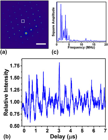
FIG. 2. Parallel-beam SAED dynamics as a function of time delay. (a) Representative UEM SAED pattern at −200 ns. Note that a negative delay denotes the amount of time remaining before photoexcitation occurs. The white box highlights the $\bar 22\bar 2$
Bragg spot. Scale bar = 5 nm−1. (b) Temporal behavior of the
$\bar 22\bar 2$
Bragg spot. Scale bar = 5 nm−1. (b) Temporal behavior of the $\bar 22\bar 2$
Bragg-spot relative intensity over the delay range −200 to 7000 ns at 2 ns increments (i.e., a UEM SAED pattern was obtained every 2 ns from −200 to 7000 ns). The Bragg-spot intensity for each time delay was normalized by the mean intensity over the entire delay range. (c) Time-domain Fourier transform of the relative-intensity trace in (b). The SAED experiments were performed using a 200 µm selected-area aperture and a 200 µm condenser aperture.
$\bar 22\bar 2$
Bragg-spot relative intensity over the delay range −200 to 7000 ns at 2 ns increments (i.e., a UEM SAED pattern was obtained every 2 ns from −200 to 7000 ns). The Bragg-spot intensity for each time delay was normalized by the mean intensity over the entire delay range. (c) Time-domain Fourier transform of the relative-intensity trace in (b). The SAED experiments were performed using a 200 µm selected-area aperture and a 200 µm condenser aperture.
B. UEM convergent-beam diffraction
With CBED, the challenges associated with extracting effects of nanoscale heterogeneity on dynamics in SAED can be circumvented. The small-probe convergent-beam configuration enables access to single-specimen-orientation 3D crystallographic information and nanoscale specimen volumes. Reference Spence and Zuo32,Reference Huang, Sun, Tao, Menard, Nuzzo and Zuo33 Fig. 3 displays the results of a nanosecond UEM CBED study on a particular volume element within the Si-cantilever region of interest studied with SAED. To extract the dynamic response of the specimen with UEM CBED, the motion of diffraction-pattern features along the corresponding reciprocal-lattice vector was followed. Under a convergent-beam condition, the Ewald sphere can be described as having a finite thickness dependent on the convergence angle of the electron beam, which effectively relaxes the Bragg condition. Reference Fultz and Howe34 Assuming a fixed-in-space electron beam, real-space specimen tilt will result in correlated motion of the reciprocal lattice, which, in this case, manifests in a CBED pattern as translation of intensity across the disc [Fig. 3(a)], corresponding to a change in excitation error. We invite the reader to compare the video of the CBED results [Supplementary Video S2] with a schematic of the effects of specimen tilting on a CBED pattern found in a standard TEM textbook to visualize the process.
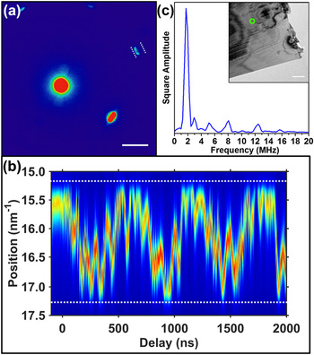
FIG. 3. CBED dynamics as a function of time delay. (a) UEM CBED pattern at −200 ns. Here, the specimen is tilted 17° off the [011] zone-axis, and the beam is converged to an angle of 5 mrad (2α). The dotted white lines denote the reciprocal-space region of interest around the 026 CBED disc. Scale bar = 5 nm−1. (b) Line scan of the 026 CBED-disc positions parallel to the reciprocal-lattice vector as a function of time delay. The position axis corresponds to the radial distance from the direct beam in the center-left of the frame. The images were acquired with a randomized time delay to compensate for any real-time beam or specimen instabilities. The position of the dotted white lines corresponds to those shown in panel (a). (c) Time-domain Fourier transform of the spatial-intensity trace shown in (b). The inset shows a UEM BF image of the specimen region of interest, with the position of the convergent beam indicated by the green circle (not to scale; actual probe diameter = 20 nm). Scale bar = 1 µm.
The temporal dependence of the translation of intensity across the CBED disc can be seen in Fig. 3(b) (see Supplementary Video S2). As in the SAED results, the primary oscillation is at 1.7 MHz. This outcome is to be expected if this frequency is indeed mechanical motion of the entire region outlined in Fig. 1(a). From both the delay trace and the time-domain Fourier spectrum, it is apparent that the higher frequency components between 10 and 15 MHz are present as well. Although UEM SAED and CBED studies capture many similar features indicative of the mechanical response, the difference in sampled volume between the two techniques is expected to lead to qualitatively and quantitatively dissimilar results, as observed here. Between 2 and 5 MHz, the SAED Fourier spectrum contains a number of distinct peaks, which are nearly as strong as the 1.7 MHz mode. In contrast, the CBED Fourier spectrum is strongly peaked at 1.7 MHz, with only two small peaks resolvable between 2 and 5 MHz. This can be at least partially attributed to the difference in the Fourier-window determining the lower spectral resolution in the CBED spectrum, as the ratio of the 1.7 MHz mode to those between 2 and 5 MHz is much higher in the CBED spectrum than in the SAED spectrum.
C. UEM BF imaging
Results from the two diffraction modalities described above suggest that the oscillatory frequencies observed in the low MHz range arise from the eigenmodes of a mesoscale cantilever. To further characterize the effects of nanoscale heterogeneity on the linear-elastic optomechanical response, UEM real-space imaging was performed on the same region of interest from which the SAED and CBED data originate (see Supplementary Video S3). In general, BF imaging involves using non-Bragg scattered electrons to form an image. In BF images of crystalline specimens, the existence of diffraction contrast allows for correlation of reciprocal- and real-space modalities, as the measured signals stem from the same interactions of the reciprocal lattice and Ewald sphere. Reference Amelinckx, Gevers and Van Landuyt35 In Fig. 4, difference images following photoexcitation are presented and compared to a reference image acquired at negative time (i.e., before photoexcitation). See the Supplementary Material for details pertaining to the image analysis methods. As can be seen, the contrast patterns, which are a function of local-specimen orientation and crystallographic order, are complex over the 5 µm2 region of interest. A portion of the entire temporal range studied, spanning from 108 to 128 ns (Fig. 4), shows one period of a contrast oscillation that was not detected in either the SAED or CBED experiments. In particular, the highlighted area indicates a diffraction-contrast feature that was observed to oscillate at 30 MHz.
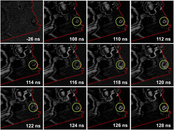
FIG. 4. Representative difference images from a UEM BF-image series. All images were binned by four and acquired with a three-second integration time. The difference images were created by first drift-correcting all images within the series, followed by subtracting a reference frame from each image. The reference frame consisted of an average of 10 pre-time-zero frames. The particular time delays at which the representative difference images were obtained are shown in the lower-right corner of each frame. The green circle highlights a strong and easily-discernible transient contrast response. The dotted red lines outline the edge of the specimen, as seen in Fig. 1(b).
By averaging over one of the spatial variables, a space–time plot can be generated, which captures aspects of the spatial variation [Fig. 5(a)]. Prior to arrival of the excitation pulse, the contrast bands remain unperturbed, though slight intensity changes due to real-time fluctuations in photoelectron beam intensity are present. Following photoexcitation, the contrast bands, particularly those at 500 and 1200 nm, begin to change x, y position as a function of time. This arises from three-dimensional motion of the specimen. In the image series, diffraction-contrast features move because specimen reorientation with respect to the fixed electron-packet wavevector produces a spatially-varying Bragg condition. Strongly-scattering dark regions become weakly-scattering bright regions as they move away from the Bragg condition, and vice versa. The oscillatory nature of this contrast motion is indicative of optomechanical excitation of the cantilever, with the period of oscillation corresponding to the period of the particular eigenmode. Further, the intensity oscillation of the Fresnel fringe is also indicative of mechanical motion as the specimen is deflected along the z-axis, thus modulating the focus condition at fixed lens strengths.

FIG. 5. Space-time analysis of the UEM BF-image series. (a) Space–time plot illustrating the oscillatory contrast behavior observed following photoexcitation of the Si cantilever. The position axis corresponds to the long axis of the red rectangle shown in the panel-(b) inset. The bright band at approximately 2 µm corresponds to a Fresnel fringe at the edge of the specimen, with vacuum at larger values. (b) Position-dependent Fourier spectrum generated from panel (a). The position axis is the same as in panel (a), and color represents frequency amplitude; warmer colors indicate larger amplitude. The inset is a UEM BF image of the Si cantilever, with the red rectangle indicating the region of interest from which panels (a) and (b) were generated.
Frequencies can be extracted at each position in the space–time plot to analyze the position-dependent frequency response [Fig. 5(b); see Supplementary Video S4]. Such an analysis reveals two large-amplitude frequency groupings, one ranging 1.5–5 MHz and another clustered around 12 MHz, as was observed with the UEM reciprocal-space modalities described above. The most prominent feature is the oscillating dark band near 1200 nm in Fig. 5(a); the feature has a primary frequency of 12.8 MHz. In addition to these cross-modality responses, however, UEM BF imaging reveals localized high-frequency modes that are not detected with the diffraction methods. The presence of large Fourier amplitudes at frequencies up to and above 30 MHz is observed nearer to the edge of the Si-wedge specimen. This suggests that additional boundary conditions stemming from nanoscale structural heterogeneity are leading to localized oscillations at the vacuum-crystal interface. While the majority of the region of interest oscillates at frequencies detected with the diffraction modalities, relatively small areas near the vacuum-crystal interface do not contribute significantly to the SAED or CBED dynamics and are thus overwhelmed by the large-amplitude lower eigenfrequencies. That is, due to spatial averaging with the selected-area aperture in SAED and the relatively small specimen volume probed in CBED, these higher-frequency energy-dissipation pathways were not detected with either diffraction technique. As positions farther from the vacuum-crystal (i.e., moving to thicker regions of the wedge) are probed, higher-frequency oscillations damp out giving way to the lower-frequency cross-modality responses.
By expanding the analysis methods used to generate Fig. 5(b) to the entire image field of view, spatial heterogeneity of the response to photoexcitation can be fully visualized through BF frequency mapping (Fig. 6). Briefly, the time-dependent images were corrected for thermal and specimen drift, after which the intensity of each pixel in each image was tracked as a function of time. By analyzing the Fourier spectrum of each pixel, spatial localization of specific linear elastic eigenmodes was tracked. A similar method has been applied to Kikuchi bands in the study of linear-elastic shear motion. Reference Yurtsever and Zewail20,Reference Yurtsever, Schaefer and Zewail21 By selecting the most prominent frequencies in the Fourier spectrum, a complete picture of the energy-dissipation pathways within the mesoscale region was generated. Selecting maps near the eigenfrequencies detected with the diffraction modalities (i.e., those below 5 MHz) reveal their spatial locations, the positions of which comprise a significant portion of the interaction volume in the SAED experiments, as defined by the selected-area aperture.

FIG. 6. Select real-space frequency maps of the optomechanical response of the Si cantilever. To generate the maps, intensity values of drift-corrected images were first normalized by the intensity over vacuum to account for beam-current fluctuations. Following this, a Fourier transform of the time-dependent intensity of each pixel was performed. Each pixel in each frame is the absolute value of the Fourier spectrum for that pixel at the particular frequency shown in the lower-left corner of each panel. Warmer colors represent larger Fourier amplitudes. The black outline denotes the edge of the specimen.
It is important to note that the dynamic contrast in the BF-imaging experiments is a function of movement through the Bragg condition; localized bending in the specimen, as seen statically in Fig. 1(b), causes dynamic contrast features to be nonuniformly distributed throughout the region of interest. Consequently, absence of BF dynamic contrast does not necessarily indicate a lack of motion, though its presence is certainly indicative of motion on at least a commensurate spatial scale. As discussed above, the higher-frequency modes localized to the lower-right portion of the specimen region within the field of view likely arise from the presence of additional boundary conditions imposed by fractures, gouges, etc. on the nanometer scale. Precise positioning of the electron-packet train for UEM CBED on specimen locations showing high-frequency responses in the BF-imaging experiments may yield similar results (see Fig. S4 in the Supplementary Material, which shows dynamics and tilting effects in three UEM CBED discs), Reference Flannigan and Zewail36 though practical challenges associated with specimen or beam drift when probing locally-isolated nanoscale areas become increasingly difficult to overcome.
D. COMSOL modeling
To model the observed linear elastic behavior of the Si cantilever, COMSOL (solid mechanics module) was used, with the specimen configured as an Euler–Bernoulli beam (Fig. 7). The dimensions of the beam were experimentally determined from the defined boundary conditions denoted by the red lines in Fig. 1(a) and the details of specimen preparation, such as estimated wedge thickness and polishing angle. The first five vibrational eigenfrequencies of our model specimen occur at 1.2, 2.0, 3.4, 4.0, and 4.23 MHz, the physical manifestations of which are shown in Fig. 7(b). Comparison of the first five eigenfrequencies obtained from the linear elastic model to the UEM-determined time-dependent response of the specimen shows reasonable agreement for frequencies below 5 MHz [Figs. 2(c) and 3(c), for example]. Frequencies above 5 MHz, observed especially in the UEM BF imaging series [Figs. 5(b) and 6], are attributed to localized mechanical vibrations [rather than motion of the entire cantilever, as outlined in Fig. 1(a)] that are a function of crystal defects near the specimen edge (e.g., fractures, gouges, bends, etc.).

FIG. 7. Linear-elastic COMSOL modeling parameters, eigenmodes, and eigenfrequencies of a model Si cantilever. (a) The dimensions of the model system, as determined with optical and electron microscopy. The cantilever was fixed on the xz face but was free on all other faces. The red box denotes the location of the BF image shown in Fig. 1(b). (b) The first five eigenmodes with frequencies labeled and displacement exaggerated for clarity. The color is a measure of the degree of deflection in the z direction; warmer colors denote a higher degree of deflection.
IV. CONCLUSIONS
The precision and ease with which electron probes can be localized on specimen regions of interest suggest UEM is well-suited for studying the effects of heterogeneously-distributed nanoscale particles and defects on constitutive relations within the mesoscale regime. Here, a multimodality approach was used to determine the time-dependent optomechanical response of a single-crystal Si cantilever. All modalities used (SAED, CBED, and BF imaging) revealed oscillatory motion in the few-MHz range, corresponding to bending eigenmodes of the cantilever. In addition, frequencies roughly five times higher than those observed with the diffraction modalities were discovered with BF imaging, analysis of which suggests local strain and structural imperfections exert nontrivial influence on the linear-elastic response. All three modalities, however, give complementary—though not necessarily matching—information, that gives insight into the dynamic processes at work. These results indicate that UEM real-space imaging, coupled with frequency-mapping methods, is useful for elucidating complex energy-dissipation pathways in defect-laden materials. It is expected that future work—both fundamental and applied—will provide additional links between structural dynamics observed with various UEM experimental modalities, as is well established for static materials-characterization methods, and that increasingly-complex specimen and device architectures will be amenable to study as the method matures and evolves.
Supplementary Material
To view supplementary material for this article, please visit http://dx.doi.org/10.1557/jmr.2016.360.
The Supplementary Material contains descriptions of the data analysis methods, details of the modeling methods, Figs. S1 through S4, and Videos S1 through S4 with captions.
ACKNOWLEDGMENTS
This work was supported primarily by the National Science Foundation through the University of Minnesota MRSEC under Award Number DMR-1420013, in part by a 3M Nontenured Faculty Award under Award Number 13673369, and in part by the Arnold and Mabel Beckman Foundation through a Beckman Young Investigator Award. We thank Prof. Vivian E. Ferry for use of her optical microscopy facilities in the Department of Chemical Engineering and Materials Science at the University of Minnesota.


 Open access