Hostname: page-component-76fb5796d-2lccl Total loading time: 0 Render date: 2024-04-28T06:59:55.432Z Has data issue: false hasContentIssue false

Resistance switching behaviors of continuous-thick hBN films fabricated by radio-frequency-sputtering

Published online by Cambridge University Press:  12 November 2020
Qiang Li
Affiliation:
Shaanxi Provincial Key Laboratory of Photonics & Information Technology, Xi'an Jiaotong University, Xi'an 710049, China School of Electronic Science and Engineering, Xi'an Jiaotong University, Xi'an 710049, China Solid-State Lighting Engineering Research Center, Xi'an Jiaotong University, Xi'an 710049, China
Xiao Qin
Affiliation:
Solid-State Lighting Engineering Research Center, Xi'an Jiaotong University, Xi'an 710049, China
Qifan Zhang
Affiliation:
School of Electronic Science and Engineering, Xi'an Jiaotong University, Xi'an 710049, China Solid-State Lighting Engineering Research Center, Xi'an Jiaotong University, Xi'an 710049, China
Yunhe Bai
Affiliation:
School of Electronic Science and Engineering, Xi'an Jiaotong University, Xi'an 710049, China Solid-State Lighting Engineering Research Center, Xi'an Jiaotong University, Xi'an 710049, China
Hua Tang
Affiliation:
School of Electronic Science and Engineering, Xi'an Jiaotong University, Xi'an 710049, China Solid-State Lighting Engineering Research Center, Xi'an Jiaotong University, Xi'an 710049, China
Chenyu Hu
Affiliation:
School of Electronic Science and Engineering, Xi'an Jiaotong University, Xi'an 710049, China
Shuoheng Shen
Affiliation:
Department of Electronic and Electrical Engineering, University of Sheffield, Mappin Street, SheffieldS1 3JD, UK
Yufeng Li
Affiliation:
Shaanxi Provincial Key Laboratory of Photonics & Information Technology, Xi'an Jiaotong University, Xi'an 710049, China School of Electronic Science and Engineering, Xi'an Jiaotong University, Xi'an 710049, China Solid-State Lighting Engineering Research Center, Xi'an Jiaotong University, Xi'an 710049, China
Feng Yun*
Affiliation:
Shaanxi Provincial Key Laboratory of Photonics & Information Technology, Xi'an Jiaotong University, Xi'an 710049, China School of Electronic Science and Engineering, Xi'an Jiaotong University, Xi'an 710049, China Solid-State Lighting Engineering Research Center, Xi'an Jiaotong University, Xi'an 710049, China
*
a)Address all correspondence to this author. e-mail: fyun2010@mail.xjtu.edu.cn
Get access

Abstract

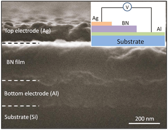
Continuous hBN films have been grown by means of a radio-frequency-sputtering technology, and their material properties have been investigated. The prepared hBN films can achieve good smoothness in a large area. The surface morphologies and compositions of the hBN films on Si substrate and Al film have been characterized, indicating that there is no difference. The 101-phase peak of hBN film is the strongest, and the optical band gap of the fabricated film is 5.84 eV. An attempt on the fabrication of the hBN based resistive switching (RS) device has been made by using an Ag/hBN/Al structure, leading to the observation of a clear and stable RS behavior. The device exhibits a resistance window (high-resistivity state/low-resistivity state) of around 102, and the RS behaviors of hBN film prepared by sputtering were first observed. It has been found that the opening voltage for the device is changed when a different cycle voltage is applied because of the built-in electric field increasing with the increase of applied cycle voltage. The mechanism of the RS behavior has been analyzed, which lay a foundation for the application of hBN as RS material in resistive random access memory to improve the storage density.

Type
Article
Copyright
Copyright © The Author(s), 2020, published on behalf of Materials Research Society by Cambridge University Press

Access options

Get access to the full version of this content by using one of the access options below. (Log in options will check for institutional or personal access. Content may require purchase if you do not have access.)

References

Park, J., Lee, S., and Yong, K.: Photo-stimulated resistive switching of ZnO nanorods. Nanotechnology 23, 385707 (2012).CrossRefGoogle ScholarPubMed
Eloi, J.C., Chabanne, L., Whittell, G.R., and Manners, I.: Metallopolymers with emerging applications. Mater. Today 11, 28 (2008).CrossRefGoogle Scholar
Qi, J., Olmedo, M., Ren, J., Zhan, N., Zhao, J., Zheng, J.-G., and Liu, J.: Resistive switching in single epitaxial ZnO nanoislands. ACS Nano 6, 1051 (2012).10.1021/nn204809aCrossRefGoogle ScholarPubMed
Waser, R. and Aono, M.: Nanoionics-based resistive switching memories. Nat. Mater. 6, 833 (2007).CrossRefGoogle ScholarPubMed
Son, J.Y., Shin, Y.H., and Park, C.S.: Bistable resistive states of amorphous SrRuO3 thin films. Appl. Phys. Lett. 92, 133510 (2008).CrossRefGoogle Scholar
Moreno, C., Munuera, C., Valenica, S., Kronast, F., Obradors, X., and Ocal, C.: Reversible resistive switching and multilevel recording in La0.7Sr0.3MnO3 thin films for low cost nonvolatile memories. Nano Lett. 10, 3828 (2010).CrossRefGoogle ScholarPubMed
Pan, F., Gao, S., Chen, C., Song, C., and Zeng, F.: Recent progress in resistive random access memories: Materials, switching mechanisms, and performance. Mater. Sci. Eng. R-Rep. 83, 59 (2014).CrossRefGoogle Scholar
Yang, J.J.S., Strukov, D.B., and Stewart, D.R.: Memristive devices for computing. Nat. Nanotechnol. 8, 13 (2013).CrossRefGoogle ScholarPubMed
Wang, H., Meng, F., Zhu, B., Leow, W.R., Liu, Y., and Chen, X.: Resistive switching memory devices based on proteins. Adv. Mater. 27, 7670 (2015).CrossRefGoogle ScholarPubMed
Tan, C.L., Liu, Z.D., Huang, W., and Zhang, H.: Non-volatile resistive memory devices based on solution-processed ultrathin two-dimensional nanomaterials. Chem. Soc. Rev. 44, 2615 (2015).CrossRefGoogle ScholarPubMed
Liang, L., Li, K., Xiao, C., Fan, S.J., Liu, J., Zhang, W.S., Xu, W.H., Tong, W., Liao, J.Y., Zhou, Y.Y., Ye, B.J., and Xie, Y.: Vacancy associates-rich ultrathin nanosheets for high performance and flexible nonvolatile memory device. J. Am. Chem. Soc. 137, 3102 (2015).CrossRefGoogle ScholarPubMed
Qian, K., Tay, R.Y., Nguyen, V.C., Wang, J., Cai, G., Chen, T., Teo, E.H.T., and Lee, P.S.: Hexagonal boron nitride thin film for flexible resistive memory applications. Adv. Funct. Mater. 26, 2176 (2016).CrossRefGoogle Scholar
Choi, B.J., Zhang, J., Norris, K., Gibson, G., Kim, K.M., Jackson, W., Zhang, M.M., Li, Z., Yang, J.J., and Williams, R.S.: Trilayer tunnel selectors for memristor memory cells. Adv. Mater. 28, 356 (2016).CrossRefGoogle ScholarPubMed
Park, S., Lee, J., Kim, H.S., Park, J.B., Lee, K.H., Han, S.A., Hwang, S., Kim, S.W., and Shin, H.J.: Formation of hexagonal boron nitride by metal atomic vacancy-assisted B-N molecular diffusion. ACS Nano 9, 633 (2015).CrossRefGoogle ScholarPubMed
Han, S.A., Lee, K.H., Kim, T.H., Seung, W., Lee, S.K., Choi, S., Kumar, B., Bhatia, R., Shin, H.J., Lee, W.J., Kim, S., Kim, H.S., Choi, J.Y., and Kim, S.W.: Hexagonal boron nitride assisted growth of stoichiometric Al2O3 dielectric on graphene for triboelectric nanogenerators. Nano Energy 12, 556 (2015).CrossRefGoogle Scholar
Lee, K.H., Shin, H.J., Lee, J., Lee, I.Y., Kim, G.H., Choi, J.Y., and Kim, S.W.: Large-scale synthesis of high-quality hexagonal boron nitride nanosheets for large-area graphene electronics. Nano Lett. 12, 714 (2012).CrossRefGoogle ScholarPubMed
Liu, Z., Song, L., Zhao, S.Z., Huang, J.Q., Ma, L.L., Zhang, J.N., Lou, J., and Ajayan, P.M.: Direct growth of graphene/hexagonal boron nitride stacked layers. Nano Lett. 11, 2032 (2011).CrossRefGoogle ScholarPubMed
Wang, H., Liu, F.C., Fu, W., Fang, Z.Y., Zhou, W., and Liu, Z.: Two-dimensional heterostructures: Fabrication, characterization, and application. Nanoscale 6, 12250 (2014).CrossRefGoogle ScholarPubMed
Shi, Y., Liang, X., Yuan, B., Chen, V., Li, H., Hui, F., Yu, Z., Yuan, F., Pop, E., Wong, H.-S.P., and Lanza, M.: Electronic synapses made of layered two-dimensional materials. Nature Electron. 1, 458 (2018).CrossRefGoogle Scholar
Wong, H.S.P., Lee, H.Y., Yu, S., Chen, Y.S., Wu, Y., Chen, P.S., Lee, B., Chen, F.T., and Tsai, M.J.: Metal-oxide RRAM. Proc. IEEE 100, 1952 (2012).CrossRefGoogle Scholar
Fantini, A., Goux, L., Degraeve, R., Wouters, D.J., Raghavan, N., Kar, G., Belmonte, A., Chen, Y.Y., Govoreanu, B., and Jurczak, M.: Intrinsic switching variability in HfO2 RRAM. A theoretical and experimental study. In 5th IEEE International Memory Workshop, P. Kalavade, ed. (IEEE, Piscataway, NJ, 2012); p. 30.CrossRefGoogle Scholar
Ji, Y., Lee, S., Cho, B., Song, S., and Lee, T.: Flexible organic memory devices with multilayer graphene electrodes. ACS Nano 5, 5995 (2011).CrossRefGoogle ScholarPubMed
Guo, N., Wei, J., Jia, Y., Sun, H., Wang, Y., Zhao, K., Shi, X., Zhang, L., Li, X., and Cao, A.: Fabrication of large area hexagonal boron nitride thin films for bendable capacitors. Nano Res. 6, 602 (2013).CrossRefGoogle Scholar
Yao, J., Lin, J., Dai, Y.H., Ruan, G.D., Yan, Z., Li, L., Zhong, L., Natelson, D., and Tour, J.M.: Highly transparent nonvolatile resistive memory devices from silicon oxide and graphene. Nat. Commun. 3, 1101 (2012).CrossRefGoogle ScholarPubMed
Tian, H., Chen, H.Y., Gao, B., Yu, S.M., Liang, J.L., Yang, Y., Xie, D., Kang, J.F., Ren, T.L., Zhang, Y.G., and Philip Wong, H.S.: Monitoring oxygen movement by Raman spectroscopy of resistive random access memory with a graphene-inserted electrode. Nano Lett. 13, 651 (2012).CrossRefGoogle Scholar
Sangwan, V.K., Jariwala, D., Kim, I.S., Chen, K.S., Marks, T.J., Lauhon, L.J., and Hersam, M.C.: Gate-tunable memristive phenomena mediated by grain boundaries in single-layer MoS2. Nat. Nanotechnol. 10, 403 (2015).CrossRefGoogle ScholarPubMed
Cheng, P.F., Sun, K., and Hu, Y.H.: Memristive behavior and ideal memristor of 1T phase MoS2 nanosheets. Nano Lett. 16, 572 (2016).CrossRefGoogle ScholarPubMed
Hui, F., Grustan-Gutierrez, E., Long, S., Liu, Q., Ott, A.K., Ferrari, A.C., and Lanza, M.: Graphene and related materials for resistive random-access memories. Adv. Electron. Mater. 3, 1600195 (2016).CrossRefGoogle Scholar
Hao, C.X., Wen, F.S., Xiang, J.Y., Yuan, S.J., Yang, B.C., Li, L., Wang, W.H., Zeng, Z.M., Wang, L.M., Liu, Z.Y., and Tian, Y.J.: Liquid-exfoliated black phosphorous nanosheet thin films for flexible resistive random access memory applications. Adv. Funct. Mater. 26, 2016 (2016).CrossRefGoogle Scholar
Li, J., Fan, Z.Y., Dahal, R., Nakarmi, M.L., Lin, J.Y., and Jiang, H.X.: 200 nm deep ultraviolet photodetectors based on AIN. Appl. Phys. Lett. 89, 3365 (2006).CrossRefGoogle Scholar
Kobayashi, Y., Akasaka, T., and Makimoto, T.: Hexagonal boron nitride grown by MOVPE. J. Cryst. Growth 310, 5048 (2008).CrossRefGoogle Scholar
Kubota, Y., Watanabe, K., Tsuda, O., and Taniguchi, T.: Deep ultraviolet light-emitting hexagonal boron nitride synthesized at atmospheric pressure. Science 317, 932 (2007).CrossRefGoogle ScholarPubMed
Pan, C., Ji, Y., Hui, F., Tang, K., Guo, Y., Xie, X., Puglisi, F.M., Larcher, L., Miranda, E., Jiang, L., Shi, Y., Valov, L., Mclntyre, P.C., Waser, R., and Lanza, M.: Coexistence of grain-boundaries-assisted bipolar and threshold resistive switching in multilayer hexagonal boron nitride. Adv. Funct. Mater. 27, 1604811 (2017).CrossRefGoogle Scholar
Ohta, J. and Fujioka, H.: Sputter synthesis of wafer-scale hexagonal boron nitride films via interface segregation. APL Mater. 5, 076107 (2017).CrossRefGoogle Scholar
Nemanich, R.J., Solin, S.A., and Martin, R.M.: Light scattering study of boron nitride microcrystals. Phys. Rev. B 23, 6348 (1981).CrossRefGoogle Scholar
Chen, T.-A., Chuu, C., Tseng, C.-C., Wen, C.-K., Philip Wong, H.-S., Pan, S., Li, R., Chao, T.-A., Chueh, W.-C., Zhang, Y., Fu, Q., Yakobson, B.I., Chang, W.-H., and Li, L.-J.: Wafer-scale single-crystal hexagonal boron nitride menolayers on Cu(111). Nature 56, 15 (2020).Google Scholar
Liang, J., Lin, J., Li, R., Song, Q., Fang, Y., Yu, C., Luo, H., Liu, Z., Tang, C., and Huang, Y.: Microstructure evolution and photoluminescence properties of boron nitride nanospheres under extreme therman processing. Ceram. Int. 43, 15402 (2017).CrossRefGoogle Scholar
Yuzuriha, T.H. and Hess, D.W.: Structural and optical properties of plasma deposited boron nitride films. Thin Solid Films 140, 199 (1986).CrossRefGoogle Scholar
Ismach, A., Chou, H., Ferrer, D.A., Wu, Y., McDonnell, S., Floresca, H.C., Covacevich, A., Pope, C., Piner, R., Kim, M.J., Wallace, R.M., Colombo, L., and Ruoff, R.S.: Toward the controlled systhesis of hexagonal boron nitride films. ACS Nano 6, 6378 (2012).CrossRefGoogle Scholar
Zhang, C.H., Fu, L., Zhao, S.L., Zhou, Y., Peng, H.L., and Liu, Z.F.: Controllable co-segregation synthesis of wafer-scale hexagonal boron nitride thin films. Adv. Mater. 26, 1776 (2014).CrossRefGoogle ScholarPubMed
Jo, S.H. and Lu, W.: CMOS compatible nanoscale nonvolatile resistance switching memory. Nano Lett. 8, 392 (2008).CrossRefGoogle ScholarPubMed
Mikheev, E., Hoskins, B.D., Strukov, D.B., and Stemmer, S.: Resistive switching and its suppression in Pt/Nb:SrTiO3 junctions. Nat. Commun. 5, 3990 (2014).CrossRefGoogle ScholarPubMed
Hu, C. and Zhu, Y.: Poly-NiO/Nb:SrTiO3 based resistive switching device for nonvolatile random access memory. Adv. Mater. Res. 605–607, 1944 (2012).CrossRefGoogle Scholar