


Introduction
Depth-sensing nano-/micro-mechanical testing of irradiated and radioactive materials has become widely utilized in scanning electron microscopic (SEM) and transmission electron microscopic (TEM) in situ configurations [Reference Kiener, Minor, Anderoglu, Wang, Maloy and Hosemann1, Reference Hosemann, Shin and Kiener2, Reference Hosemann3]. An advantage of these in situ methods is that the experimentalist can obtain quantitative load–displacement data alongside real-time video that informs deformation phenomena at SEM/TEM resolutions. The specimen size effect [Reference Arzt4, Reference Nix and Gao5, Reference Elmustafa and Stone6, Reference Kiener, Grosinger, Dehm and Pippan7, Reference Nowak, Beaber, Ugurlu, Girshick and Gerberich8, Reference Greer and De Hosson9, Reference Ngan, Chen, Leung, Gu and Gan10] cannot be neglected when reducing mechanical testing geometries to the SEM/TEM scale. The size effect is evidenced by elevated yield stress measurements in successively smaller specimen geometries and is attributed to the specimen geometry being sufficiently small that it contains too few dislocation sources, inhibiting plastic yield until a sufficient population of dislocations has been introduced through external loading. However, the presence of irradiation-induced defects and/or nanostructuring sufficiently reduce the intrinsic dimension (i.e., microstructure) of the material, such that an electron-transparent extrinsic dimension (i.e., specimen geometry) can provide meaningful mechanical tests using the in situ TEM approach [Reference Wharry, Yano and Patki11].
A variety of in situ TEM specimen geometries have been demonstrated on irradiated materials, including indentation [Reference Yano, Thomas, Swenson, Lu and Wharry12], tensile [Reference Ding, Tian, Han, Li, Ma and Shan13, Reference Chisholm14], bending and fracture [Reference Han, Ding and Shan15], and compression pillars [Reference Kiener, Hosemann, Maloy and Minor16, Reference Mao, Özerinç, King, Averback and Dillon17, Reference Yano, Swenson, Wu and Wharry18, Reference Jawaharram, Price, Barr, Hattar, Averback and Dillon19, Reference Patki20]. Uniaxial compression pillars are among the most commonly used specimen geometries because their stress state is relatively easy to understand compared to indentation, and they are relatively easy to fabricate as compared to tensile, bend, and fracture geometries [Reference Hosemann, Shin and Kiener2]. Kiener et al. [Reference Kiener, Hosemann, Maloy and Minor16] published the first TEM in situ compression pillar study on an irradiated material. That work investigated the minimum pillar dimensions that would provide meaningful mechanical test results (i.e., representative of bulk mechanical test results) from irradiated Cu. Subsequently, several groups have utilized the approach to quantitatively understand deformation in a number of materials. Dillon and coworkers have used TEM in situ compression pillars to study shear strengths of irradiated Cu–Nb interfaces [Reference Mao, Özerinç, King, Averback and Dillon17] as well as the behavior of irradiation-induced creep in Ag [Reference Jawaharram, Price, Barr, Hattar, Averback and Dillon19]. Yano et al. [Reference Yano, Swenson, Wu and Wharry18] and Patki [Reference Patki20] have used TEM in situ compression pillars to understand yield strength in irradiated Fe–9% Cr oxide dispersion strengthened (ODS) and nanocrystalline Cu–24% Ta alloys, respectively.
The TEM in situ compression pillar studies on irradiated materials have thus far focused primarily on elastic and yield properties (with the exception of the irradiation-induced creep study, Ref. Reference Jawaharram, Price, Barr, Hattar, Averback and Dillon19), the measurement of which is relatively straightforward. Engineering stress–strain curves are simple to generate from load–displacement data collected from in situ TEM since they require knowledge of only the initial specimen dimensions and cross-sectional area. Subsequently, properties such as yield strength and elastic modulus can be measured directly from the engineering stress–strain curve [Reference Yano, Swenson, Wu and Wharry18]. But beyond the elastic and yield properties from engineering stress–strain curves, TEM in situ mechanical testing has the potential to enhance our understanding of plastic phenomena which are critical to comprehensively evaluating irradiated materials performance. Studying plastic phenomena (e.g., work hardening) is more complex and requires an understanding of true stress–strain behavior. Generating these true stress–strain curves can be challenging because they require knowledge of the instantaneous specimen dimensions throughout loading.
With the widespread adoption of nano-/micro-mechanical materials testing techniques over the past decade, numerous methods have been developed to generate true stress–strain curves and measure local stresses and strains from SEM or TEM in situ videos, recently summarized in Ref. Reference Gammer, Richard and Eberl21. Many of these methods are based on digital image correlation (DIC) techniques [Reference Kuo, Zaefferer, Zhao, Winning and Raabe22, Reference Godara, Raabe, Bergmann, Putz and Muller23, Reference Kamaya and Kawakubo24, Reference Zhu, Bai, Zhang, Lei and He25]. Specifically, a photogrametric pixel-based pattern recognition algorithm is used, which maps the microtexture onto a finite element mesh [Reference Raabe, Sachtleber, Zhao, Roters and Zaefferer26]. This requisite coupling with a finite element model is critical for mapping stresses and strains across a microstructure. However, there remains an opportunity for generating a true stress–strain curve in a simpler, self-contained, and more automated manner.
In this paper, we present an automated method for processing TEM in situ micropillar compression test videos to extract the instantaneous pillar dimensions and then determine the true stress–strain curves. This method is benchmarked for the TEM in situ micropillar compression tests previously published by the authors on as-received and ion-irradiated model Fe–9% Cr ODS alloy and nanocrystalline Cu–24% Ta. The strain hardening coefficients are extracted from the true stress–strain curves and are discussed in the context of the deformation mechanisms observed concurrently in the TEM in situ videos.
Results
Summary of elastic and yield properties from compression pillar tests
TEM in situ compression pillars were used to measure the elastic properties, including modulus and yield strength, of the as-received, 3 and 100 dpa-irradiated Fe–9% Cr ODS [Reference Yano, Swenson, Wu and Wharry18]. Elastic moduli measured directly from the TEM in situ compression tests were adjusted for deformation and deflection in the base material and then fell within a range of 130–309 GPa, consistent with the expected values [Reference Yano, Swenson, Wu and Wharry18]. Irradiation had little to no effect on the elastic modulus [Reference Yano, Swenson, Wu and Wharry18]. Compression yield stress values were also relatively unaffected by irradiation [Reference Yano, Swenson, Wu and Wharry18] and were consistent with the expected values for minimum pillar dimensions larger than ∼100 nm [Reference Toualbi, Cayron, Olier, Logé and de Carlan27]. The Cu–24% Ta compression yield stress values were also unchanged with 1 dpa irradiation [Reference Patki20]. All pillars, even those with external dimensions ≤100 nm, have yield stresses near the expected bulk yield stress because of the ∼nm scale of the Cu–24% Ta microstructure [Reference Wharry, Yano and Patki11].
The absence of statistically significant irradiation strengthening in both the ODS and Cu–24% Ta was consistent with the observed microstructure stability in both materials and can be explained by the enhanced kinetics at the 500 °C irradiation temperature. Negligible irradiation hardening is typical of 500 °C irradiations in a variety of Fe–Cr alloys including a model Fe–9 Cr alloy self-ion irradiated to 1 dpa [Reference Heintze, Bergner and Hernández-Mayoral28], F82H irradiated with Fe3+ to 5 dpa [Reference Ando, Tanigawa, Jitsukawa, Sawai, Katoh, Kohyama, Nakamura and Takeuchi29], tempered martensitic HT-9 proton irradiated to 2 dpa [Reference Hosemann, Vieh, Greco, Kabra, Valdez, Cappiello and Maloy30], and T91 proton irradiated to 3 dpa [Reference Penisten31].
True stress–strain curves and strain hardening exponents
To gain insight into plastic deformation, true stress–strain curves are generated for each compression pillar experiment using the algorithm described in section “True stress–strain curves and strain hardening exponents.” with “Algorithm to automate true stress–strain calculation.” Representative pairs of engineering and true stress–strain curves are shown for each material condition in Figs. 1 and 2 for the ODS and Cu–24% Ta, respectively. The true stress–strain curves are identical to the engineering stress–strain curves through the elastic region, but the curves deviate from one another upon plastic yielding. The pillar barreling (i.e., increasing pillar width and thickness) during plasticity causes the true stresses to be lower than engineering stresses, and true strains to be larger than engineering strains. As is common in nanosized pillars and wires, the stress–strain curves tend to exhibit three regions: (i) linear elastic, (ii) strain hardening immediately upon plastic yielding, and (iii) plastic yielding at constant or gradually decreasing flow stress [Reference Champion, Guérin-Mailly, Bonnentien and Langlois32, Reference Philippe, Wang, Peyrot, Hassel and Michler33]. These three distinct regions, marked in Fig. 2(a) as an example, are more clearly evident in the true than in the engineering stress–strain curves.

Figure 1: Representative engineering (dashed) and true (solid) stress–strain curves from (a) as-received, (b) 3 dpa, and (c) 100 dpa Fe–9% Cr ODS micropillars.

Figure 2: Representative engineering (dashed) and true (solid) stress–strain curves from (a) as-received and (b) 1 dpa Cu–24% Ta micropillars.
The strain hardening (or softening) exponent, n, describes the deformation characteristics of a material and is obtained from the true stress–strain curves. The Matlab™ algorithm developed herein uses linear regression to calculate the strain hardening exponent based on the user-identified strain range of interest:
 $$\sigma = K{\varepsilon ^n}\quad ,$$
 $$\log \left( \sigma \right) = n \times \log \left( \varepsilon \right) + \log \left( K \right)\quad .$$
In the Fe–9% Cr ODS, the as-received pillars tend to exhibit low but positive strain hardening exponents, with an average value of 0.16. But after irradiation, the average strain hardening exponents are reduced and become negative, with average values of −0.21 and −0.25 for the 3 dpa and 100 dpa specimens, respectively. Hence, irradiation induces strain softening in the Fe–9% Cr ODS. In the Cu–24% Ta, on the other hand, strain hardening coefficients are negative even in the as-received material (average value −0.21). Irradiation does not measurably alter the strain hardening coefficient for Cu–24% Ta (average value −0.24), and the strain softening behavior persists. Strain hardening exponents of both the Fe–9 Cr ODS and Cu–24% Ta appear to be independent of strain rate, at least within the narrow strain rate range tested, 0.005–0.025 s−1 (Fig. 3). Meanwhile, the strain hardening exponent for Fe–9 Cr ODS is dependent on the specimen minimum dimension, Fig. 3(c), although this trend does not hold for the Cu–24% Ta [Fig. 3(d)].
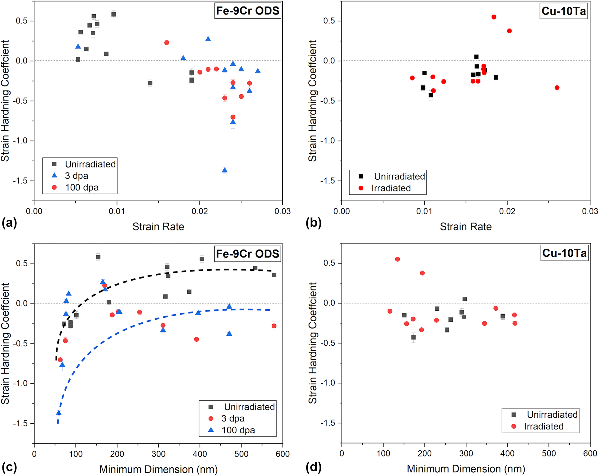
Figure 3: Strain hardening exponent as a function of strain rate for (a) ODS and (b) Cu–24% Ta, and as a function of minimum pillar dimension for (c) ODS and (d) Cu–24% Ta.
TEM video
The true stress–strain curves also obviate the numerous load drops that occur throughout deformation in both as-received and irradiated alloys. In the Fe–9% Cr ODS, load drops appear to be associated with dislocation bursts. One such burst is depicted in still-frames from the TEM resolution video of the as-received Fe–9% Cr ODS [Figs. 4(a)–4(c)], in which a band of dislocations moves through the material at time coincident with a load drop in the true stress–strain curve. But with irradiation, possible dislocation cross-slip is observed in Fe–9% Cr ODS. Specifically, ‘U’-shaped dislocations moving upward [one such dislocation is identified with an arrow in Figs. 4(d) and 4(e)] cross-slip and become lines moving northwest [Figs. 4(f) and 4(g)].
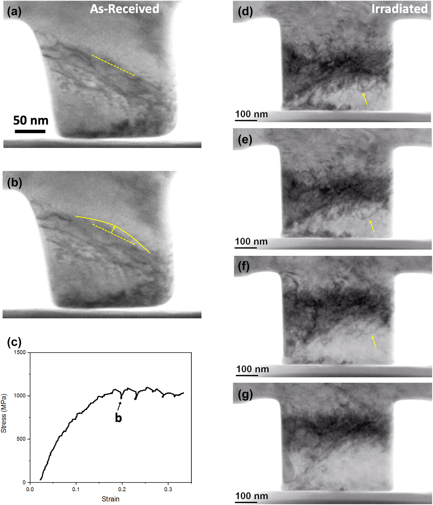
Figure 4: Still-frames from TEM in situ compression pillar test on as-received Fe–9% Cr ODS, showing strain burst (a and b) corresponding to load drops on the true stress–strain curve (c); and still-frames from TEM in situ compression pillar test on 3 dpa, 500 °C, Fe2+ irradiated Fe–9% Cr ODS, showing dislocation in (d and e) cross-slipping in (f and g).
In the Cu–24% Ta, the load drops are believed to be associated with grain boundary sliding events. For example, in the irradiated Cu–24% Ta, still-frames from the TEM video show grain boundary sliding at a triple junction [Figs. 5(a)–5(c)] following dislocation-mediated triple junction displacement that is characteristic of grain boundary sliding [Reference Ovid’ko, Pande and Masumura34]. Two of the three boundaries comprising the triple junction exhibit sliding, with each boundary’s motion corresponding to a load drop in the true stress–strain curve [Fig. 5(d)].

Figure 5: (a–c) Still-frames from TEM in situ compression pillar test on 1 dpa, 500 °C proton-irradiated Cu–24% Ta, showing two-step grain boundary sliding of the yellow (b) and pink (c) boundaries at a triple junction, corresponding to load drops on the engineering stress–strain curve (d).
Discussion
Bulk compression tests for the Cu–24% Ta show a small amount of strain hardening at the onset of plasticity, followed by pronounced strain softening [Reference Darling, Tschopp, Guduru, Yin, Wei and Kecskes35]. This complex behavior is relatively consistent with the generally negative strain hardening coefficients measured from as-received and irradiated Cu–24% Ta compression pillars herein. Likewise, the strain hardening coefficients from most of the as-received Fe–9% Cr ODS pillars fall reasonably near the bulk values of ∼0.2–0.4 as measured by nanoindentation in Refs. Reference Dolph, da Silva, Swenson and Wharry36 and Reference Robertson, Panigrahi, Balaji, Kataria, Serruys, Mathon and Sundar37. However, the strain hardening coefficients from the irradiated Fe–9% Cr ODS pillars are notably lower than bulk values. But it is well known that nano- through micro-scale mechanical tests are currently unable to extract meaningful “bulk” hardening parameters [Reference Dehm, Jaya, Raghavan and Kirchlechner38]. The miniaturized specimen geometry [Reference Dunstan and Bushby39, Reference Kiener and Minor40] and the microstructure-controlled localized plastic phenomena most significantly influence the strain hardening coefficient measured in nano-/micro-mechanical tests. These factors will be considered in the remainder of this section.
Intermitted plastic flow
Intermitted stress–strain curves, with load drops associated with isolated slip events or strain bursts, are well known to occur during deformation of nano- through micro-scale specimens [Reference Dimiduk, Woodward, LeSar and Uchic41]. These isolated strain bursts in microcompression pillars have also been linked to strain softening [Reference Schneider, Kaufmann, Clark, Frick, Gruber, Mönig, Kraft and Arzt42]. Low strain hardening exponents and strain softening are also common in materials undergoing localized deformation [Reference Jiang, Jonas, Luo, Sachdev and Godet43]; this behavior tends to be exacerbated with irradiation [Reference Farrell, Byun and Hashimoto44]. Strain softening due to strain localization has been observed and predicted in a wide variety of irradiated materials including Fe and steels [Reference Farrell, Byun and Hashimoto44, Reference Barton, Arsenlis and Marian45], Zr alloys [Reference Farrell, Byun and Hashimoto44], Cu [Reference Blewitt, Coltman, Jamison and Redman46], Mo [Reference Brimhall47], Ni [Reference Okada, Kanao, Yoshiie and Kojima48], and Au [Reference Okada, Kanao, Yoshiie and Kojima48]. Likewise, in unirradiated materials, low strain hardening or strain softening due to localized deformation has been observed in materials prehardened by cold working [Reference Choi, Liu, Sun and Khaleel49, Reference Ritschel, Luft and Schulze50, Reference Yoshida, Kiritani, Deguchi and Kamigaki51, Reference Cottrell and Stokes52], quenching [Reference Yoshida, Kiritani, Deguchi and Kamigaki51, Reference Mori and Meshii53], or precipitation [Reference Mori and Meshii53, Reference Gysler, Lütjering and Gerold54], which tend to have the effect of locking dislocations and dislocation sources. Strain burst-based load drops during deformation are consistent with observations from the TEM video collected during the Fe–9% Cr ODS compression tests (Fig. 4). These load drops typically occur when dislocation sources, once activated, send avalanches of dislocations through the material. These avalanches sweep out the barriers ahead of them, clearing a soft pathway resulting in strain softening [Reference Cottrell and Stokes52]. Other proposed explanations include rapid dislocation release and movement [Reference Hahn55], cascade-induced source hardening [Reference Singh, Foreman and Trinkaus56], and geometrical softening [Reference Price and Kelly57].
Strain softening
The microstructure is believed to be central to the strain hardening/softening behavior in the as-received and irradiated Fe–9% Cr ODS. Dislocation dynamics models have provided plausible explanations for both oxide nanocluster-induced strain hardening and strain softening. For example, incoherent oxide nanoclusters cause strain hardening as mobile dislocations pinch off into Orowan loops around them [Reference Bakó, Weygand, Samaras, Chen, Pouchon, Gumbsch and Hoffelner58]. On the other hand, incoherent oxide nanoclusters can also force mobile dislocations to cross-slip around them [Reference Robertson and Gururaj59], resulting in little strain hardening. Both of these explanations could be at work in the as-received Fe–9% Cr ODS, justifying the low strain hardening measured.
Irradiation induces strain softening in the Fe–9% Cr ODS, which can be attributed to irradiation-induced oxide disordering and dislocation loop nucleation and growth. We have shown that the oxide nanoclusters in the same 3- and 100-dpa specimens studied herein undergo inverse Ostwald ripening during irradiation [Reference Swenson and Wharry60]. Inverse Ostwald ripening occurs due to competing irradiation damage mechanisms of ballistic dissolution and diffusion-driven nanocluster growth [Reference Wharry, Swenson and Yano61]. In the most extreme cases, inverse Ostwald ripening is evidenced by a reduced average cluster size and increased number density, but during its evolutionary stages, the phenomenon presents as enhanced incoherency, disordering, irregularity, or “haloing” at the oxide–matrix interface [Reference Dubuisson, Schill, Hugon, Grislin, Seran, Nanstad, Hamilton, Garner and Kumar62, Reference Lescoat, Ribis, Gentils, Kaïtasov, De Carlan and Legris63, Reference Zhanbing, Benfu, Kinoshita, Takahashi and Watanabe64]. As these oxide–matrix interfaces become increasingly diffuse and incoherent, dislocation cross-slip around them becomes more likely and common [Reference Robertson and Gururaj59], further reducing strain hardening. Another theory from Robertson and Gururaj [Reference Robertson and Gururaj59] considers the concomitant roles of oxide nanoclusters and irradiation-induced dislocation loops. In the presence of loops, dislocations accumulate around oxides, generating high internal stresses and leading to cross-slip. With the help of internal stresses, cross-slipped dislocations can then overcome dislocation loops, reducing strain hardening. This can explain the possible cross-slip behavior observed in the TEM in situ compression video of the irradiated Fe–9% Cr ODS (Fig. 4). Our prior TEM in situ indentation tests [Reference Yano, Thomas, Swenson, Lu and Wharry12] also corroborate the idea that dislocation loops play a central role in deformation of the same irradiated Fe–9% Cr ODS studied here.
The low strain hardening and strain softening observed in the Cu–24% Ta specimens are typical of nanostructured and nanocrystalline materials [Reference Lu, Chen, Huang and Lu65, Reference Zhu and Liao66, Reference Kumar, Van Swygenhoven and Suresh67] because nanocrystalline grains are inherently unable to accumulate dislocations, unless dislocation motion can be obstructed through pinning, tangling, or locking [Reference Wu, Zhu, Wei and Wei68]. Rather, in nanocrystalline materials, grain boundary dislocation emission and absorption occur readily because of the high number density of grain boundaries [Reference Chen, Ma, Hemker, Sheng, Wang and Cheng69, Reference Zhang, Liu, Wang, Li, Sun and Ma70, Reference Van Swygenhoven, Derlet and Frøseth71, Reference Yamakov, Wolf, Phillpot, Mukherjee and Gleiter72], leading to deformation by grain boundary sliding and migration [Reference Gutkin, Ovid’ko and Skiba73, Reference Yu, Peng and Wen74, Reference Padmanabhan, Dinda, Hahn and Gleiter75, Reference Guo, Song, Luo, Goddard, Chen, Reddy and An76, Reference Zelin and Mukherjee77] or grain rotation [Reference Yamakov, Wolf, Phillpot, Mukherjee and Gleiter72, Reference Wang, Teng, Liu, Hirata, Ma, Zhang, Chen and Han78, Reference Schiotz79, Reference Van Swygenhoven and Derlet80, Reference Cahn and Taylor81, Reference Wolf, Yamakov, Phillpot, Mukherjee and Gleiter82, Reference Farkas, Mohanty and Monk83]. Similarly, micropillar compression and nanoindentation studies of Al/Al3Sc [Reference Han, Phillips and Nix84], Al/Nb [Reference Li, Wang, Huang, Misra and Zhang85], Cu/Zr [Reference Zhang, Lei, Liu, Niu, Chen, Liu, Zhang and Sun86], and Cu/Nb [Reference Mara, Bhattacharyya, Hirth, Dickerson and Misra87, Reference Mara, Bhattacharyya, Dickerson, Hoagland and Misra88] nanolayers exhibit strain softening when nanolayer thicknesses are on the order of a few tens of nm. Dislocation emission and absorption readily occur at nanolayer interfaces, with little to no dislocation accumulation within the layers. The softening is subsequently attributed to slip on the interlayer planes [Reference Mara, Bhattacharyya, Hirth, Dickerson and Misra87].
These typical mechanisms of strain softening are consistent with the evidence of grain boundary sliding shown in our irradiated Cu–24% Ta TEM in situ compression pillars (Fig. 5). The absence of an irradiation-induced change in strain hardening exponent for Cu–24% Ta is consistent with the negligible irradiation-induced microstructure evolution [Reference Patki20]. Hence, the extreme irradiation tolerance attributed to the nanocrystallinity of the Cu–24% Ta limits the extent of structure–property evolution under irradiation.
Parametric dependences of strain hardening exponents
The observation that strain hardening exponents are independent of strain rate (Fig. 3) is consistent with arguments presented by Dunstan and Bushby [Reference Dunstan and Bushby39] and Kiener and Minor [Reference Kiener and Minor40], which state that the parameters that most strongly influence strain hardening exponent are the specimen geometry and the flow strain. It is expected that the strain hardening exponent for Fe–9 Cr ODS will be dependent on the specimen minimum dimension [Fig. 3(c)]. The size effect on strain hardening can be explained because at very small specimen dimensions, there are insufficient defects in the material—so once dislocations are nucleated, they can glide easily without getting hung up on defects, hence the absence of the typical work hardening behavior. But the observed independence of the Cu–24% Ta strain hardening exponent on the specimen dimension [Fig. 3(d)] is believed to be caused by the extremely nanoscopic characteristic length of the microstructure (∼20 nm) [Reference Wharry, Yano and Patki11], which is smaller than even the smallest pillar dimensions tested (∼75 nm). The same phenomenon has been observed for the Cu–24% Ta yield stress measured by TEM in situ compression pillars, in which an absence of a transition between size-effected and “bulk-like” yield stresses was observed [Reference Wharry, Yano and Patki11] due to the nanoscopic characteristic length, i.e., intrinsic size, of the microstructure.
Conclusions
We have analyzed the plastic deformation of as-received and irradiated Fe–9% Cr ODS and nanocrystalline Cu–24% Ta, following TEM in situ compression pillar testing. We have developed an algorithm to automate the measurement of instantaneous pillar dimensions, which enabled us to generate true stress–strain curves for each pillar. Intermitted plastic flow is observed in all as-received and irradiated specimens of both Fe–9% Cr ODS and Cu–24% Ta. This behavior is typical of nano- through micro-scale specimens and is directly linked to strain bursts in the Fe–9% Cr ODS as observed in TEM videos.
Strain hardening coefficients were calculated for each pillar. Values of the strain hardening exponent were low to negative for all specimen conditions, indicative of low strain hardening to strain softening. In Fe–9% Cr ODS, irradiation induces strain softening due to the irradiation-induced disordering of oxide nanoclusters and nucleation of dislocation loops. In the Cu–24% Ta, the strain softening is attributed to grain boundary sliding, which is directly observed in the TEM videos during compression testing. Strain hardening exponents are generally independent of strain rate, but are influenced by specimen dimensions.
Methods
Materials, irradiations, and micropillar compression testing
This work analyzes the stress–strain response of TEM in situ compression pillars of two irradiated nanostructured alloys: an Fe–9% Cr ODS steel and a Cu–24% Ta nanocrystalline alloy (compositions in wt%). Here, we will summarize the materials, their irradiations, and their microstructures.
The Fe–9% Cr ODS was obtained from the Japan Nuclear Fuel Cycle Development Institute (now known as the Japan Atomic Energy Agency). The ODS alloy was processed by mechanical alloying of ferritic steel with Y2O3 powder, followed by 1150 °C hot extrusion. The final heat treatment involved 1-h solutionizing at 1050 °C, air cooling, 800 °C tempering, and a final air cooling. The composition in wt% of major components is Fe–8.67, Cr–1.96, W–0.23, Ti–0.27, Y–0.14, O–0.14, C–0.34, and Y2O3. Complete details of the fabrication and processing of the ODS alloy can be found in Ref. Reference Ohtsuka, Ukai, Fujiwara, Kaito and Narita89. Specimens of the ODS alloy were irradiated with 5.0 MeV Fe2+ ions to doses of 3 and 100 displacements per atom (dpa) at 500 °C. To achieve these doses, total ion fluences of 4.0 × 10¹⁵ and 1.3 × 10¹⁷ ions/cm2 were delivered, respectively, at a dose rate of 2.2 × 10⁻⁴ dpa/s. The irradiation damage profile was calculated using the Stopping Range of Ions in Matter (SRIM) 2013 in quick Kinchin–Pease mode, per Ref. Reference Stoller, Toloczko, Was, Certain, Dwaraknath and Garner90. The nominal doses of 3 and 100 dpa were determined at a depth of 400–600 nm into the damage profile, which avoids both surface and ion implantation effects as recommended by Zinkle and Snead [Reference Zinkle and Snead91]. Comprehensive irradiation experiment details can be found in Refs. Reference Yano, Swenson, Wu and Wharry18 and Reference Dolph, da Silva, Swenson and Wharry36.
The starting microstructure of the ODS alloy is comprised of ∼230 nm fully martensitic grains containing a dislocation density of ∼19 × 1014 m−2 and ∼6 nm oxide nanoclusters at a number density of ∼57 × 1022 m−3 [Reference Swenson and Wharry92]. There are no statistically significant irradiation-induced changes in grain size and dislocation density [Reference Swenson and Wharry60, Reference Swenson and Wharry93]. However, both the 3- and 100-dpa irradiations induce the nucleation of ∼10 nm dislocation loops at number densities on the order of ∼1021 m−3. The oxide nanocluster number density decreases by a factor of four in the 3-dpa irradiation condition [Reference Swenson and Wharry60, Reference Swenson and Wharry93]. The comprehensive microstructure quantification from Refs. Reference Swenson and Wharry60 and Reference Swenson and Wharry93 is summarized in Table I, with example micrographs shown in Figs. 6(a) and 6(b).
TABLE I: Quantitative summary of microstructure of materials tested.
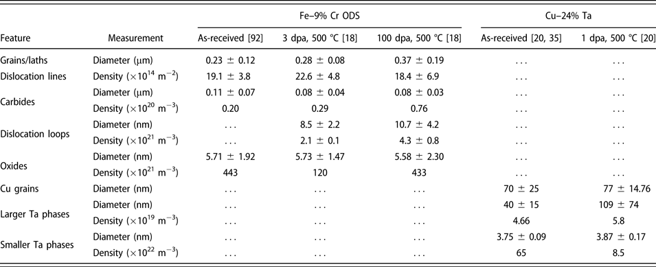

Figure 6: Representative bright-field TEM micrographs of (a) as-received and (b) irradiated Fe–9% Cr ODS, with red arrows indicating oxide nanoclusters and dashed red circles indicating dislocation loops; and (c) as-received and (d) irradiated Cu–24% Ta, with yellow arrows indicating Ta nanoclusters  $\lessapprox$ 20 nm and solid yellow circles indicating Ta phases $\gtrapprox$ 20 nm. Composition of Ta phases and nanoclusters in irradiated Cu–24% Ta is confirmed by (e) zero loss image and (f) EFTEM.
The Cu–24% Ta is a binary nanocrystalline alloy, studied as a simple model system of engineering ODS alloys. The Cu–24% Ta was obtained from the US Army Research Laboratory and was synthesized by high-energy cryogenic mechanical alloying of immiscible Cu and Ta powders. As-milled powders were consolidated by equal channel angular extrusion (ECAE) at 700 °C using a channel angle of 90°. Four consecutive extrusions produced a total strain of ∼450% in the material. Comprehensive details on the Cu–24% Ta alloy processing are available in Ref. Reference Darling, Tschopp, Guduru, Yin, Wei and Kecskes35. The as-extruded microstructure contains ∼70 nm metallic Cu grains, with a bimodal metallic Ta particle size distribution having mean values around 7 and 40 nm [Reference Darling, Tschopp, Guduru, Yin, Wei and Kecskes35]. The Cu–24% Ta was irradiated with 2.0 MeV protons to 1 dpa at 500 °C. To achieve this dose, a total ion fluence of 7.6 × 10¹⁸ protons/cm2 was delivered, and the dose rate was 7.3 × 10⁻⁵ dpa/s. The irradiation damage profile was calculated using SRIM 2013 in quick Kinchin–Pease mode, and the nominal dose of 1 dpa was determined at a depth of 10 μm (i.e., approximately half the distance to the damage peak). The Cu–24% Ta was irradiated concurrently with specimens analyzed in Ref. Reference Bazarbayev, Kattoura, Mao, Song, Vasudevan and Wharry94, which provides more comprehensive details of the proton irradiation experiments. No statistically significant grain or phase size evolution was observed after irradiation, and sparse irradiation-induced defects were reported in the Cu grains [Reference Patki20]. The microstructure quantification is summarized in Table I, with example micrographs in Figs. 6(c) and 6(d). The chemical composition of Cu grains and Ta phases and nanoclusters is confirmed using energy filtered TEM (EFTEM), Figs. 6(e) and 6(f).
Micropillars having rectangular cross-sections were fabricated from the as received and irradiated Fe–9% Cr ODS and Cu–24% Ta using focused ion beam (FIB) milling. Micropillar dimensions were systematically varied between 60 and 700 nm to understand the role of extrinsic size effects. Corners and edges of pillars having rectangular cross-sections are known to introduce stress concentrations that influence elastic properties and yield stress [Reference Kiener and Minor40, Reference Lowry, Kiener, Leblanc, Chisholm, Florando, Morris and Minor95]. But since the present work focuses on the plastic region of the stress–strain curve, stress concentrations at pillar corners and edges are not considered in the strain hardening analysis. The external dimensions were verified by TEM and thickness by electron energy loss spectroscopy (EELS). A minimum of 10 micropillars were tested from each material condition. Micropillars were compressed to half of their original height using a diamond flat punch tip on a Hysitron (now Bruker, Minneapolis, Minnesota) PI-95 depth-sensing TEM mechanical testing holder. Throughout each compression test, quantitative load and displacement data were collected along with TEM-resolution video at a frame rate of 30 frames per second (fps). Strain rates ranged 0.01–0.026 s−1. Engineering stress–strain curves were generated for each pillar, from which the elastic moduli and 0.2% offset yield stress were determined. Moduli and yield stresses for the ODS were reported in Ref. Reference Yano, Swenson, Wu and Wharry18, and yield stresses for the Cu–24% Ta were reported in Ref. Reference Patki20.
Algorithm to automate true stress–strain calculation
To calculate the true stress and strain, we developed an algorithm within Matlab™ to automate the measurement of instantaneous pillar widths throughout the compression test. The algorithm was comprised of two major tools, executed in sequence: (i) image processing to determine pillar widths from TEM video, and (ii) data analysis to calculate true stress–strain curves. A flowchart of the algorithm is shown in Fig. 7.
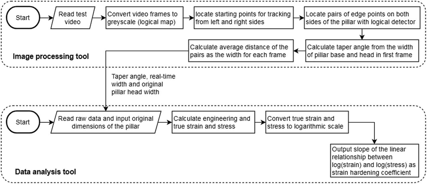
Figure 7: Flowchart of Matlab™ algorithm developed to automate pillar width determination and true stress–strain curve calculation.
Within the image processing tool, each frame of the TEM video was first converted to a greyscale image. The canny edge detection routine, built-in within Matlab™, applied a Gaussian filter to the image; the derivative of the Gaussian filter was used to identify local maxima. These local maxima were edges or boundaries of features within the original TEM video frame. For the purposes of this study, these identified “edges” were the true edges of the pillar, as well as some of the highest-contrast features within the pillar microstructure (e.g., grain boundaries, precipitates, dislocation loops). Based on the edge identification, a pixel-by-pixel binary numerical map was generated, wherein pixels containing an identified edge were marked as 1 and are colored white, while all other pixels were marked as 0 and were colored black.
Once the pixels in each frame are color-coded, a logical filter is used to identify pillar dimensions. A logical filter moves downward from the top left and top right corners of the image to identify pixels surrounded by all black (or 0) pixels. These pixels are set as the starting points for the edge tracking algorithm and are marked as ‘+’ in Fig. 8; these points ensure the pillar edge tracking begins in the TEM vacuum, rather than on the specimen or flat punch. From the starting points, the script moves toward the center of the image until it encounters pillar edges, marked as ‘×’ in Fig. 8. The script then moves onto each subsequent row of pixels in the binary numerical map and scans from both sides until it marks five or more points (based on user preference), or until it reaches the upper or lower boundary of the TEM vacuum. After five pairs of edge points are marked, the distance between each pair is calculated, and the average of these distances is exported as the instantaneous pillar width; this is repeated for each frame of the video. On only the first frame of the video, the pillar base and head (marked as ‘o’ in Fig. 8) widths are specifically measured for calculating taper angle as:
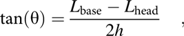 $$\tan \left( \theta \right) = {{{L_{{\rm{base}}}} - {L_{{\rm{head}}}}} \over {2h}}\quad ,$$
where L base is the width of the pillar at contact with the substrate, L head is the pillar width at contact with the indentation head, and h is the height of the pillar.

Figure 8: Application of edge tracking algorithm to a frame that has been converted to binary (black and white) image, with the starting points for the edge tracking algorithm marked ‘+’, pillar edges marked ‘×’, and pillar base and head marked ‘○’.
The second component of the script calculates true stress and strain hardening exponent. The raw load–displacement data obtained from the experiment is read in to Matlab™. The user specifies the original pillar dimensions, and the instantaneous pillar widths (for each frame) are called from the image analysis portion of the script. Engineering stress and strain are first calculated based on original pillar dimensions, and the elastic modulus is determined. True stress and strain are calculated at each time step (i.e., in each frame), based on the instantaneous pillar dimensions and using expressions developed by Zhang et al. [Reference Zhang, Liang, Zhang, Wu, Liu and Sun96] for multicrystalline micropillars under compression:
 $${\varepsilon _{\rm{T}}} = {{1 + {{{L_0}} \over {{r_{{\rm{head}}}}}}\tan \left( \theta \right)} \over {{E_{{\rm{measured}}}}}}{{P{L_{{\rm{final}}}}} \over {{A_{{\rm{half}}}}{L_0}}} + \ln \left( {{{{L_0}} \over {{L_{{\rm{final}}}}}}} \right)\quad ,$$
 $${\sigma _{\rm{T}}} = {P \over {{A_{{\rm{half}}}}{L_0}}}\left\{ {{L_0} - \left[ {{u_{{\rm{tot}}}} - {{P\sqrt \pi \left( {1 - {v^2}} \right)} \over {2{E_{{\rm{substrate}}}}\sqrt {{A_{{\rm{base}}}}} }}} \right]} \right\}\quad ,$$
where L 0 is the initial pillar height, A half is the pillar cross-sectional area at half the initial pillar height, L final is the final pillar height, r head is the radius at the top of the pillar, u tot is the total displacement, and A base is the average cross-sectional area of the substrate. Although the compression pillars studied in this work have rectangular cross-sections, the automated method presented can be utilized on pillars with round cross-sections and can also be extended to SEM in situ compression pillar testing.
Supplementary material
To view supplementary material for this article, please visit https://doi.org/10.1557/jmr.2019.295.
Acknowledgments
This research was sponsored in part by the National Science Foundation CAREER award DMR-1752636, the US Department of Energy Office of Nuclear Energy awards DE-NE0008758 and DE-NE0008759, Purdue University, and by the US DOE Office of Nuclear Energy under DOE Idaho Operations Office contract DE-AC07-05ID14517, as part of the Nuclear Science User Facilities experiments 16-656 and 18-1168.


 Open access