

Introduction
Layered semiconductor materials have attracted considerable attention in the past 10 years for the fabrication of electronic devices such as transistors, energy storage batteries, and other photovoltaic and catalytic engineering applications.[Reference Kumar Singha, Kumar, Late, Kumar, Patel and Singh1,Reference Li and Zhu2] The MoS2 crystal structure was resolved by Pauling and Dickinson,[3,Reference Dickinson and Pauling4] who were able to determine S–Mo–S sandwich layers as stacked in three layers over the c-axis by a van der Waals weak bonding creating a unit cell.[Reference Dickinson and Pauling4] MoS2 lattice parameters are always a = b = 3.17 Å, whereas the c-axis varies according to the found polyforms 2H-MoS2 (hexagonal, c = 12.3 Å), 3R-MoS2 (rhombohedral, c = 18.3 Å), and 1T-MoS2 (trigonal).[Reference Ramos, Chianelli, Enríquez-Carrejo, Gonzalez and Berhault5,Reference Ramos, Galindo-Hernández, Arslan, Sanders and Domínguez6] MoS2 theoretically predicted and experimentally verified band gaps range from 0.8 to 1.9 eV as extensively discussed in the literature.[Reference Perea-López, Lin, Pradhan, Iñiguez-Rábago, Elías, McCreary, Lou, Ajayan, Terrones, Balicas and Terrones7] Observations of the MoS2 structure on the transmission electron microscopy (TEM) level were first made by Chianelli et al. confirming an average ~0.62 nm distance between MoS2 layers.[Reference Chianelli, Ruppert, José-Yacamán and Váquez-Zavala8] Garcia et al. performed a TEM experiment to determine radiation damage under Cs-corrected TEM observations encountering that 80 kV is appropriate to achieve a good observation on single layers, which were able not to obtain any three-dimensional (3D) information.[Reference Garcia, Raya, Mariscal, Esparza, Herrera, Molina, Scavello, Galindo, José-Yacamán and Ponce9] And, using the computer software, Wu et al. estimated the sample thickness versus contrast by ADF-STEM and SAED simulations.[Reference Wu, Odlyzko and Andre Mkhoyan10] Even though TEM is a highly sophisticated microanalysis tool, it is only possible to achieve 2D imaging,[Reference Egerton, McLeod, Wang and Malac11] and while electron tomography by TEM can be applied to obtain volume distribution of MoS2 thin films and particles, it is limited to −30° to +30° of probe tilting, as described by Kong et al.[Reference Kong, Wang, Cha, Pasta, Koski, Yao and Cui12] Compared to that, laser-assisted atom probe tomography (APT) is a characterization technique to determine the chemical and spatial resolution at the 3D nanometric scale. For example, APT was used to determine titanium homogeneous spatial (3D) distribution within a MoS2 matrix on magnetron-sputtered thin films, as reported by Singh et al.[Reference Singh, Mutyala, Evans and Doll13] Also, it was used to obtain a spatial distribution on SiGe/Si/SiGe interfaces, in order to determine any migration and volume distribution between species.[Reference Dyck, Leonard, Edge, Jackson, Pritchett, Deelman and Poplawsky14] Here, APT measurements of molybdenum disulfide (MoS2) layers on indium tin oxide (ITO) are presented. ITO was selected for the electrical contact layer because of its low resistivity n-type semiconductor behavior having 2–4 × 10⁻⁴ Ω cm together with other beneficial electronic properties. The optimum electrical properties of ITO can be achieved through post-deposition annealing of the film at temperatures between 300 and 500°C, and it is highly used as a transparent contact material for the integration and fabrication of electronic devices like graphic display panels, photovoltaic panels, and nanotransistors.[Reference Szász, Seils, Klotz, Störmer, Heilmaier, Gerthsen, Yokokawa and Ivers-Tiffée15–Reference Marikkannan, Subramanian, Mayand, Tanemura, Vishnukanthan and Pearce19] In our study, a metal-semiconducting interface was studied using APT to determine any possible migration/precipitation of indium (In), tin (Sn), oxygen (O2), molybdenum (Mo), and sulfur (S) species, which in principle could affect electron mobility. The long-term motivation of this work is the fundamental understanding of layered MoS2 templates for low-cost solar cells fabrication.
Materials and methods
ITO and MoS2 were deposited directly onto commercial APT coupons (Cameca©) as substrates using a Kurt J. Lesker PVD-75 RF-magnetron sputtering located in a class 1000 clean room (S1). The ITO deposition period was 1800 s with a sputter gas mixture of 90% Ar and 10% O2 at 20°C, 3 mT at 145 W DC. To maintain consistently low ITO resistivity, O2 was only introduced during the deposition period of the processing sequence. Prior to and following the deposition phase, 100% Ar was utilized to stabilize the target's surface prior to deposition and in preparation for subsequent runs. After deposition, the ITO film was subjected to a rapid thermal annealing process, 300°C for 20 min at atmospheric pressure using a 100 sccm gas mixture of 3.8% H2/Balance N2. The subsequent MoS2 deposition period was 3600 s using 100% Ar at 20°C, 3 mT at an applied power of 275 W DC. The aforementioned deposition conditions achieved an MoS2 layer with a thickness of approximately 700 nm. The film surface was observed using a scanning electron microscopy (SEM) model Hitachi SU5500 equipped with energy-dispersive x-ray unit and operated at 20 kV with 8 A to avoid sample damage. The 3D spatial distribution of S, Mo, In, Sn, and O2 was studied by an APT technique, using a Cameca® LEAP 4000X high-resolution system, equipped with a UV laser (λ ~ 355 nm). All measurements were taken at a set temperature of 50 K with an evaporation rate of 0.2 and a laser frequency of 100 kHz. The laser beam was set to 20 pJ/V, and all data were reconstructed from SEM images using the Cameca IVAS© 3.6.14 package. Additional samples were prepared by directly coating the microtip coupons provided by the CAMECA with the multilayer sputtering system. The samples were prepared by annular milling with the aid of the focused ion-beam (FIB) instrument models FEI© Strata or Zeiss Auriga, both equipped with dual beam. The surface was protected with an additional platinum layer deposited from a precursor gas within the SEM-FIBs to reduce amorphization of the MoS2 film matrix due to Ga-ion beam radiation; FIB was carried out with 1000–100 pA ion beam gun power. The grazing-incidence x-ray diffraction (GIXRD) was performed in a Rigaku Smart Lab with a HyPix 3000 detector and Cu Kα radiation source. The sample was aligned using the Rx–Ry stage, parallel beam with PA-optics, and an incident angle of 0.2° or 0.5°. The detector was in the point detector 0D mode, texture analysis was completed with 5° Soller slits on beam side and detector side, slits on detector side are open (10 mm), speed 50°/min, the detector in the area 2D mode.
Results and discussion
Using SEM during FIB needle preparation for APT measurements, it was possible to observe a typical high porosity MoS2 film matrix surface (Fig. 1(a)). A direct deposit on pristine APT coupons was done due to the fragility seen during the FIB lift-out process from deposits made on SiO2 (images are presented in the Supplementary material); thus, a reduction of amorphization over ITO–MoS2 interface was achieved. Amorphization is typical, mainly in semiconductors as extensively described by Bogdanowicz et al. for silicon (Si) and gallium nitride (GaN) thin films during the FIB lift-out process.[Reference Bogdanowicz, Kumara, Fleischmann, Gilbert, Houard, Vella and Vandervorst20] Vertical nucleation and growth oriented along the 〈110〉-MoS2 direction of neddle-like crystallites over the silicon substrate using similar RF-sputtering conditions have been previously reported by Ramos et al.,[Reference Ramos, Nogan, Ortíz-Díaz, Enriquez-Carrejo, Rodríguez-González, Mireles-Jr-Garcia, Ornelas and Hurtado-Macias21] and it is presented in Figs. 1(a)–1(d). The GIXRD principal reflections at (002) which corresponds to 2H-MoS2 stacks (wire thickness), (100) and (101) and (201) indicate space group 2H-R3 m and average crystallite size of 6.216 Å and d (101) = 2.838 Å, as shown in Fig. 2(a) (insets: enlargement at (101)-principal reflection). This is in agreement with the results of Lince and Fleischauer and Jiang et al. for heterogenous MoS2/WS2 heterojunctions.[Reference Lince and Fleischauer22,Reference Jiang, Sun, Song, Dou, Ji and Wang23] And we found no substantial evidence of 1T and 2H mixed-phase formed during sputtering, as recently reported by Sarma et al.[Reference Sarma and Chandra Ray24] SEM images indicate that rugosity [Fig. 2(c)] and elemental analysis by surface energy-dispersive x-ray emission confirmed the presence of S and Mo as shown in Fig. 2(d). A full description of the APT technique is beyond this report, but in brief it consists of placing a sample to undergo an ionizing evaporation process by the laser pulse at a high electric field under UHV conditions and low temperatures. Then, the potential energy of an ion leaving the sample's surface is due to the shape of the field almost entirely converted into kinetic energy of 1/2 mv 2 in the close vicinity of the tip. Thus, to obtain the mass-spectra signal, the relationship given by m/n = 2e/d 2(Vdc)t 2 is used to analyze the mass- to charge-state ratio (m/n) of ions evaporated; n is the number of electrons removed from an ion, e the electron charge (−1.62 × 10⁻¹⁹C), V dc is the applied voltage, m is the atomic mass, and the speed of an ion is given as v = d/t, with d being the distance detector-tip and t is the time of flight (a schematic of test set-up is presented in Supplementary material).[Reference Kelly and Miller25] The results from APT measurements indicate a well-defined interface between MoS2 and ITO layers as shown in Fig. 3(a); allowing to observe a well-defined chemical contact of MoS2 and the ITO matrix (Supplementary video), with little, to no intermixing within chemical species. From the time-of-flight mass spectra, as shown in Fig. 3(b), it was possible to determine that sulfur and molybdenum tend to evaporate as MoS molecular ions (MoS+2, MoS+3,  ${{{\rm MoS}_3}^{+2}}$, and MoS+1). Due to its typical peak fingerprint, these molecules, as well as Sn, can be identified easily and are used to track the respective element distributions. Indium has only one major isotope, but it does not show any overlaps with any other possible peaks from ITO and MoS2, and thus the corresponding atoms can be identified with certainty. The most problematic overlap for this material is between S+ and
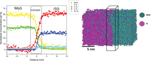
  ${{{\rm O} _2}^+}$. Here, it is necessary to disregard the main peak for both 32 amu and the minor peak at 33 amu. By contrast, the peak at 34 amu almost exclusively stems from S and can be used to track its position. The same problem exists for the double-charged ion S2+. However, the isotope at 17 amu cannot be used because it overlaps with OH+. In Fig. 4, the proxigram profile through the 50 at.% indium isosurface is shown, and it was utilized to identify the ITO–MoS2 interface concentration along the vertical growth direction and more detailed volume reconstruction is presented in Fig. 4(b). It was calculated with a bin size of 0.1 nm as a function of the distance from the isosurface. The high spread of the S and O concentration results from the necessity to disregard the main S/O2 peak at 32 amu in the mass spectrum. Together with the subsequent background correction, this causes the originally—in absolute values—small errors for S and O concentrations to spread to values that can even be negative for O. The continuous lines through the data points illustrate the concentration gradient without this effect.

Figure 1. (a) SEM image for ITO–MoS2 as-deposited over commercial APT pristine coupons. (b) SEM image of the tiny needle as completed by FIB is possible to determine the layers; by contrast, the red arrow indicates some porosity. (c) A sharper needle used to perform the APT measurements. (d) Brightness profile along the tip axis between left-ITO center–MoS2 and right-ITO coating [as denoted by a red dotted line on (c)]. Each portion of ITO measures ~100 nm, while the MoS2 layer measures ~ 700 nm.

Figure 2. (a) GIXRD pattern and pole figures for MoS2 as-deposited over ITO; (b) pole figures and predominant diffraction for (101) indicating a vertical alignment of MoS2 crystallites in agreement with the literature[Reference Lince and Fleischauer22]; (c) SEM image for the MoS2 surface; it is possible to observe vertical laminar structures typical of MoS2 (inset: colored signals of the Mo and S content as obtained by EDS), in agreement with Lince and Fleischauer[Reference Lince and Fleischauer22]; and (d) energy-dispersive x-ray spectroscopy (EDS) taken from MoS2 surfaces during the SEM survey (inset: an enlarge region near 2.1 keV where S-KA1 and Mo-LA1 signals overlap).

Figure 3. (a) APT distribution for the ITO–MoS2 interface. MoS2 is displayed as small spheres 16S cannot be distinguished from 16O2 easily in the mass spectrum, as they both have a signal at 32 amu. Every single dot represents one atom, and for visibility, only 20% of In atoms are displayed with no enrichment found within the ITO–MoS2 interface. (b) Mass spectrum of the ITO–MoS2 interface. Due to the complexity of the mass spectra, only the peaks near 60 amu were identified as MoS contributions mainly and used for the APT reconstruction. Other peaks were identified as O, Sn, In, SnO, InO, SnS, InS, SO, and Mo.

Figure 4. (a) Proxigram of relative composition for S, O2, Mo, In, and Sn as data processed taken from the interaction at the interface. (b) APT time-of-flight volume reconstruction for ITO and MoS2 interface. (c) Spatial atomic reconstruction for the MoS2 matrix from APT measurements. No specific features were encountered. (d) Raman spectroscopy performed over the MoS2 film surface, typical two main vibrational modes at E12g at 378 cm−1 and A1g at 407 cm−1 are found in agreement with the literature.[Reference Kong, Wang, Cha, Pasta, Koski, Yao and Cui12,Reference Sarma and Chandra Ray24]
In our APT study, it was mainly intended to be able to distinguish the existence of 1T and 2H phases within the MoS2 film matrix with a spatial distribution map-based approach as described by Boll et al.[Reference Boll, Al-Kassab, Yuan and Liu26,Reference Boll, Zhu, Al-Kassab and Schwingenschlög27] and Geiser et al.,[Reference Geiser, Kelly, Larson, Schneir and Roberts28] since evidence of its existence was reported by x-ray photon spectroscopy (XPS).[Reference Sarma and Chandra Ray24] However, the aberrations during ions trajectory, due to limited APT precision in the laser mode, made it difficult to achieve an accurate reconstruction of the tip surface.[Reference Gault, Moody, de Geuser, Tsafnat, La Fontaine, Stephenson, Haley and Ringer29] Moreover, the high fragility of the tips, specially at high vacuum conditions, did not allow us to achieve a large collection of time-of-flight events to complete statistical analysis. The spatial distribution of S and Mo is given in Fig. 4(c), which indicates no segregation or migration of In, Sn, or O2 from the ITO layer. And, using Raman surface spectroscopy, we were able to confirm the formation of the 2H-MoS2 phase, due to modes of vibration at E12g at 378 cm−1 and A1g at 407 cm−1 at the surface as presented in Fig. 4(d), and previously discussed in Ref. [Reference Ramos, Nogan, Ortíz-Díaz, Enriquez-Carrejo, Rodríguez-González, Mireles-Jr-Garcia, Ornelas and Hurtado-Macias21].
Conclusions
We successfully presented RF-sputtering of 2H-MoS2 thin films over the ITO substrate from commercial 99.9% targets. Our results from Raman spectroscopy and GIXRD indicated large colonies of 2H-MoS2 crystallites with epitaxial growth along 〈101〉. By SEM, it was possible to observe large colonies of flakes with porosity within. APT allowed us to determine spatial distribution reconstruction of the ITO–MoS2 interfaces, and this reconstruction shows no indication of segregation of any specific element within the film matrix and interface. The proxigram concentration profiles confirmed the uniform composition of MoS2 and ITO layers. The obtained information from APT measurements indicates that ITO can serve as an ideal transparent contact material, suggesting that the semiconducting electronic structure properties will be retained in multilayers of MoS2–ITO.
Supplementary material
The supplementary material for this article can be found at https://doi.org/10.1557/mrc.2019.150.
Acknowledgments
The principal author, M. Ramos, thanks the Karlsruhe Micro and Nano Facility (KNMF) of Karlsruhe Institute of Technology for the usage of atom probe tomography and FIB instruments under proposal 2018-020-022609. The KNMF grants measurement time to external users for proposals pertinent to KNMF goals. The authors would like to express their gratitude to Delphine Chassaing from KIT for the APT–FIB preparation. Universidad Autónoma de Ciudad Juárez for financial support by PIVA-2017 project titled: “Fabricación de plantillas metálico-orgánicas: Una ruta hacia celdas solares más eficientes.” And to UACJ-PFCE-1337 scholar travel award from UACJ. Part of this work was performed at the Center for Integrated Nanotechnologies, an Office of Science User Facility operated for the U.S. Department of Energy (DOE) Office of Science. Sandia National Laboratories is a multi-program laboratory managed and operated by Sandia Corporation, a fully owned subsidiary of Lockheed Martin Corporation, for the U.S. Department of Energy's National Nuclear Security Administration under contract DE-AC04-94AL85000.


 Open access