


Introduction
With the development of society, demands for new materials applied in energy- and sensor-related area have become more and more urgent [Reference Zhao, Liu, Zhu, Xu, Li, Huang, Zhang and Liu1, Reference Lee, Kim, Park, Park, Lee and Jeong2]. The concept of “nanostructure” was first proposed in 1959 [Reference Huang and Mei3], and has become one of the most promising materials because of their nanoscale properties and high controllability. The materials with nanostructures have one or three dimensions in the scale of 1–100 nm [Reference Liu, Liu, Liu, Du, Wang and He4, Reference Jin, Guo, Liu, Liu, Vasileff, Jiao, Zheng and Qiao5]. Hierarchical nanostructured materials are composites comprised with various functional phases and interfaces [Reference Huang, Cavallo, Liu and Lagally6, Reference Zheng, Tang, Li, Hu, Zhang, Xue and Pang7, Reference Fang, Kim, Kim and Yu8, Reference Ding, Zhang, Chen and Lou9]. In the resultant hierarchical nanomaterials, combination of different phases with electrical/magnetic/mechanical/optical functions leads to new properties that cannot be found in conventional materials [Reference Radovic, Dubourg, Dohcevic-Mitrovic, Stojadinovic, Vukmirovic, Samardzic and Bokorov10, Reference Janghela, Devi, Kambo, Roy, Mukhopadhyay and Prasad11, Reference Cheng, Chang, Feng, Jian, Wu, Zheng, Wang, Ma, Xu, Song, Wang and Zhang12, Reference Abu-Zied and Alamry13]. However, the fabrication of composite structure through the combination of functionalized phases or confined different nanomaterials in space of few nanometers is still very challenging [Reference Zhu, Chen, Yang, Cai, Bao and Zhou14]. One of the challenges in the fabrication of novel nanostructures is the direct manipulating of atoms, which can preserve the properties of both nanomaterials when combining those to form a new composite structure [Reference Pimenta, Dresselhaus, Dresselhaus, Cancado, Jorio and Saito15, Reference Dai, Jiao, Ma, Zeng, Lu, Wang, Bao and Zhai16, Reference Linic, Christopher and Ingram17, Reference Li, Mueller, Gilje, Kaner and Wallace18]. One common strategy for constructing composite structures is the deposition of nanoparticles or monolayers on the surfaces of substrates [Reference Oviroh, Akbarzadeh, Pan, Coetzee and Jen19]. Various deposition approaches, such as solution-based precipitation [Reference Sutka, Jarvekulg and Gross20], sol–gel method [Reference Zhang, Yang, Sun and Wang21], layer-by-layer (LBL) deposition [Reference Yang, Gong, Zhang and Que22], electrodeposition [Reference Nazari, Kashanian and Mohammadi23], chemical vapor deposition (CVD) [Reference Dawood, Gupta, Monteverde, Alqahtani, Kim, Sexton, Young, Missous and Migliorato24], and atomic layer deposition (ALD) [Reference Oviroh, Akbarzadeh, Pan, Coetzee and Jen19], have been explored. Among all the deposition methods, ALD is one of the most promising deposition techniques due to good conformality, excellent thickness and composition controlability, and ability of manipulation at atomic scale [Reference Tseng, Wuu, Chen, Lee, Chien, Liu and Horng25, Reference Lee, Lee, Park, Yu, Cho, Kim and Cha26], and therefore has become a promising technique in nanostructure fabrications. In ALD-related researches, a wide range of materials and structures such as various wafers [Reference Kim, Chang, Cho, Kim, Kim, Choi, Ko, Hwang and Park27], nanoparticles [Reference Zhu, Liu and Sun28], nanowires [Reference Solanki, Huo, Freeouf and Miner29], nanotube [Reference Ahmed, Xia and Alshareef30], soft materials [Reference Chen, Kang, Hirahara, Aisawa and Li31], and biological materials [Reference Knez, Kadri, Wege, Gosele, Jeske and Nielsch32], can be served as substrates for ALD coating. The resultant nanostructures are applied for enhanced performance in batteries [Reference Li, Meng, Liu, Geng, Zhang, Banis, Li, Yang, Li, Sun, Cai and Verbrugge33, Reference Jung, Cavanagh, Riley, Kang, Dillon, Groner, George and Lee34], supercapacitors [Reference Sun, Xie, Wang, Sun, Cavanagh, Travis, George and Lian35, Reference Guan, Xia, Meng, Zeng, Cao, Soci, Zhang and Fan36, Reference Boukhalfa, Evanoff and Yushin37], catalysts [Reference van der Zande, Huang, Chenet, Berkelbach, You, Lee, Heinz, Reichman, Muller and Hone38, Reference Hofmann, Sharma, Ducati, Du, Mattevi, Cepek, Cantoro, Pisana, Parvez, Cervantes-Sodi, Ferrari, Dunin-Borkowski, Lizzit, Petaccia, Goldoni and Robertson39, Reference Zhao, Zhang, Zhao, Liu, Liu, Wang, Zheng, Huang and Mei40], and sensor areas [Reference Ratan, Kumar, Kumar, Jarwal, Mishra, Upadhyay and Jit41, Reference Huang, Chang, Chang, Lee, Chang, Kwo, Wu and Hong42].
Along this review article, the function and the applications of ALD will be discussed. The first part of the article illustrates the history and advantages of ALD, focusing on its function for nanostructure fabrication. Then, the applications in supercapacitor and battery will be demonstrated. Sensor and especially biosensor applications of ALD-fabricated nanostructures are subsequently summarized. Finally, the outlook and conclusion will describe the perspectives and challenges of ALD method in terms of nanostructure fabrication and processing.
History and advantages of ALD
ALD is a technique enabling a variety of thin film materials coating from the vapor phase [Reference Huang, Cavallo, Liu and Lagally6, Reference Knoops, Donders, Baggetto, Sanden, Notten and Kessels43]. ALD was first invented by Finland physicist Tuomo Suntola in 1977, which was called atomic layer epitaxy (ALE) [Reference Oviroh, Akbarzadeh, Pan, Coetzee and Jen19]. Depositions of ZnS, SnO2, and GaP layers through vapor phase on glass plate were achieved via this method [Reference Reghima, Akkari, Guasch and Kamoun-Turki44, Reference Nasr, Kamoun and Guasch45, Reference Baek, Jin, Lee, Jeong, Lee and Lee46]. In the next decades and up to now, the synthesis strategy was then referred to as ALD [Reference George47]. A typical ALD cycle consists of two gaseous chemical precursors that perform self-limiting reactions with each other on certain substrates and one precursor is firstly pulsed into the reactor chamber to adsorb on the surface of substrate under vacuum [Reference Puurunen48, Reference Groner, Fabreguette, Elam and George49]. The reactions between precursors and active groups on the substrate are self-limiting, whereas the surplus precursor molecules and the intermediate products are removed by inert carrier gas purging (commonly N2 or Ar) [Reference Groner, Fabreguette, Elam and George49]. Only one monolayer is generated on the surface of substrate eventually. The next step involves the purging of a second chemical precursor gas to react with the molecules coating on substrate to form the resultant layer [Reference Wellings, Chaure, Heavens and Dhannadasa50, Reference Schreier, Heroguel, Steier, Ahmad, Luterbacher, Mayer, Luo and Gratzel51, Reference Niinisto, Paivasaari, Niinisto, Putkonen and Nieminen52, Reference Guan, Wang, Zhang, Fan, Zhang and Fan53]. Subsequently, after purging of carrier gas again, the untreated precursors and intermediate products are removed. Therefore, only one monolayer of desired material is deposited on the substrate in one cycle and the thickness of obtained film/membrane can be well controlled by tuning the number of cycles [Reference Zhao, Gao, Li, Song, Hu and Liu54, Reference Szabo, Volk, Horvath, Medveczky, Czigany, Vad and Baji55].
The major advantage of ALD is the controllability at atomic scale control due to its sequential, self-saturating, vapor phase reaction [Reference Zhu, Liu and Sun28, Reference Tynell and Karppinen56, Reference Kozen, Lin, Pearse, Schroeder, Han, Hu, Lee, Rubloff and Noked57]. Compared with other deposition techniques, the conformality of nanomembrane deposited via ALD is the crucial feature [Reference Robertson58, Reference Park, Yoon and Thomas59, Reference Golberg, Bando, Huang, Terao, Mitome, Tang and Zhi60]. The unique characteristic broadens its applications in decorating and modifying three-dimensional structures. With sufficient waiting times of precursors pulsing, the precursor can penetrate into deep structure, leading to complete membrane coating on the entire surface [Reference King, Heineman, Graugnard and Summers61]. On the other hand, sequential deposition induces the uniform growth on various structures, whereas other deposition techniques, for example, CVD, may hardly generate such uniform layer due to rapid surface reactions and shadowing effects [Reference Kwack and Choi62]. In a typical ALD cycle, only finite surface sites can be adsorbed, and therefore the reactions only produce a finite number of surface species. The self-limiting reaction between precursors can produce a thin layer at atomic level control in a sequential deposition process. Thus, an apparent advantage of ALD is the highly controllable of thickness when depositing membranes. Through the regulation of cycling number of ALD process, the thickness of film can be tailored. In the single depositing process, ultrathin layer with thickness about or even less than 1 Å can be fabricated [Reference Leskela and Ritala63]. In addition, composition control is another obvious advantage of the ALD technique [Reference Kim, Vaynzof, Sepe, Guldin, Scherer, Cunha, Roth and Steiner64, Reference Gregorczyk, Kozen, Chen, Schroeder, Noked, Cao, Hu and Rubloff65, Reference Bae, Shin and Nielsch66]. Composition control has been illustrated with a variety of materials such as zinc oxide (ZnO), aluminum oxide (Al2O3), or titanium dioxide (TiO2), and others [Reference Huang, Chang, Chang, Lee, Chang, Kwo, Wu and Hong42, Reference Zhang, Zhao, Whitney, Elam and Van Duyne67, Reference Ritala, Kukli, Rahtu, Raisanen, Leskela, Sajavaara and Keinonen68, Reference Bonera, Scarel and Fanciulli69]. These membranes can be deposited and compositionally controlled via precursors choosing in ALD process. For example, to produce multiple nanostructures with ZnO and Al2O3 composite layer, the component of resultant membrane can be adjusted through changing the cycle ratios between ZnO and Al2O3 [Reference Johansson, Kostamo, Karppinen and Niinisto70, Reference Yang, Wolcott, Wang, Sobo, Fitzmorris, Qian, Zhang and Li72, Reference Miikkulainen, Leskela, Ritala and Puurunen73], which can regulate and combine various properties of the materials such as conductive performance [Reference Yin, Wu, Zhou, Huang, Zhang, Boey and Zhang74, Reference Choi, Jeong, Kim, Rohde, Choi, Oh, Kim, Hwang, Szot, Waser, Reichenberg and Tiedke75], pseudocapacitive property [Reference Daubert, Mundy and Parsons76], or optical characteristic [Reference Banerjee, Lee, Bae, Lee and Rubloff77]. Figure 1 shows a collection of electron microscopy images of nanostructures, in which ALD was used in at least one of the fabrication steps.
Complex nanostructures synthesized by ALD. (a) Pt nanotube structure observed inside porous anodic alumina template cross‐section. Adapted from Ref. Reference Comstock, Christensen, Elam, Pellin and Hersam141. (b) ZnO nanomembrane obtained with 200 ALD cycles. The inset shows the ZnO nanomembranes in a vial. Adapted from Ref. Reference Zhao, Huang, Li, Edy, Gao, Tang, Bao and Mei150. (c) CNT@Co3O4 on CC. Adapted from Ref. Reference Guan, Qian, Wang, Cao, Zhang, Li and Wang127. (d) Nanoporous gold films after CoO deposition. Adapted from Ref. Reference Zhang, Huang, Qian, Yuan, Wang and Chen136. (e) 2D honeycomb lattice photonic crystal fabricated in an air-bridge format. Adapted from Ref. Reference Cha, Lee, Jordan, Lee, Oh, Kim, Park, Hong and Jeon138. (f) Ni grown on CNTs after 250 cycles of ALD (as illustrated in the inset). Adapted from Ref. Reference Choi, Kim, Lee, Kim, Choi, Kim, Kim, Park and Kim135. (g) C/ZnO porous network of the sample after pyrolysis. Adapted from Ref. Reference Zhao, Huang, Wang, Ma, Fan, Bao and Mei79. (h) Rat cortical neuron on the sensor input structure of a CMOS FG FET chip, which was passivated by an Al2O3/HfO2 multilayer. Adapted from Ref. Reference Schindler, Kim, Hwang, Schindler, Offenhaeusser and Ingebrandt81. (i) Conical Al2O3 replicas obtained by coating the conical nanochannels by 150 cycles of ALD Al2O3. Adapted from Ref. Reference Wang, Fu, Wang, Kong, Sheng, Wang, Chen and Xue139.

Because of its unique advantages, ALD technique may play an essential role in energy storage and sensing fields. Herein, we summarize the concrete function of this method via selective examples. We will focus on the applications in supercapacitors, batteries, and sensors (including biosensors). Our reviews on the applications of ALD for nanostructures are summarized as follows:
Growth and deposition of active materials
Because of the strong combination between ALD coatings and substrate, active materials can be directly deposited as functional body on certain substrate with good characteristic. The active materials include uniform nanomembrane or nanoparticle, which can provide desired properties like high catalytic activity, good conductivity, outstanding capacitance, or bio compatibility [Reference Yang, Tong, Wang, Gao, Guo and Qin78, Reference Zhao, Huang, Wang, Ma, Fan, Bao and Mei79, Reference Naeem, Naeem, Zhao, Wang, Zhang, Mei and Huang80]. Such applications commonly involve a one-pot synthesis via ALD deposition, which is convenient and efficient [Reference Zhu, Liu and Sun28, Reference Naeem, Naeem, Zhao, Wang, Zhang, Mei and Huang80]. The quantity and morphology of active materials are also simple to control through adjusting the deposition process, and it is easy to establish the relation between structure and property.
Formation of the protective layer
The uniform and firm films can be used as a protective layer to separate active component and harsh environment. For example, the corrosion from electrolyte will degrade the electrochemical performance of electrode, whereas ALD coatings can prevent the structure from destroying [Reference Schindler, Kim, Hwang, Schindler, Offenhaeusser and Ingebrandt81, Reference Couniot, Vanzieleghem, Rasson, Van Overstraeten-Schloegel, Poncelet, Mahillon, Francis and Flandre82]. In addition, the nanomembrane can efficiently reduce the dissolution of active materials [Reference Im, Lindquist, Lesuffleur and Oh83]. In the biosensor-related field, maintaining the characteristic stability of biologic active molecule such as enzyme, antibody, biotin, and certain proteins is especially critical [Reference Tereshchenko, Fedorenko, Smyntyna, Konup, Konup, Eriksson, Yakimova, Ramanavicius, Balme and Bechelany84, Reference Dominik, Lesniewski, Janczuk, Niedziolka-Joensson, Holdynski, Wachnicki, Godlewski, Bock and Smietana85, Reference Wang, Lin, Huang, Lu, Lue, Yang, Pijanswska, Yang, Wang, Yu, Chang, Chou and Lai86]. The protective shell formed by the ALD technique has become a promising strategy.
Direct establishment of nanoarchitecture
ALD technique can participate in the establishment of nanoarchitecture, owing to its fascinating conformal depositing advantage. For example, one may utilize area selective ALD deposition to generate certain pattern or step [Reference Couniot, Vanzieleghem, Rasson, Van Overstraeten-Schloegel, Poncelet, Mahillon, Francis and Flandre82, Reference Lee, Zine, Baraket, Zabala, Campabadal, Caruso, Trivella, Jaffrezic-Renault and Errachid87], and nanoarchitectural materials can be elaborated by ALD [Reference Zhao, Huang, Wang, Ma, Fan, Bao and Mei79, Reference Xie, Choi, Lu, Roling, Herron, Zhang, Park, Wang, Kim, Xie, Mavrikakis and Xia88, Reference Mayrhofer, Mitterer, Hultman and Clemens89, Reference Marichy, Bechelany and Pinna90]. During the vapor phase penetration, nanomembrane can form in deep channel of substrate, which broadens the applications of ALD technique from two-dimensional plate to three-dimensional framework. On the other hand, the substrates of ALD coatings can also be used as sacrificial templates to produce self-standing layer [Reference Zhu, Wu, Liu, Lu, Zhang, Fan and Ding91, Reference Purniawan, Pandraud, Moh, Marthen, Vakalopoulos, French and Sarro92].
Applications of ALD in batteries
Batteries, which are considered as successful and promising energy storage devices for the future development, such as lithium-ion batteries (LIBs), lithium–sulfur batteries (LSBs), sodium-ion batteries (NIBs), and zinc–air batteries [Reference Dunn, Kamath and Tarascon93, Reference Scrosati and Garche94, Reference Wang, Yang, Wan, Du, Xie and Xu95, Reference Kundu, Talaie, Duffort and Nazar96, Reference Fu, Cano, Park, Yu, Fowler and Chen97] have been deeply investigated in mechanism, materials, and applications, owing to their high energy capacity, excellent storage density, low-self discharging, splendid stability, and so forth [Reference Lang, Xiao, Gu, Guo, Wen and Wan98, Reference Nitta, Wu, Lee and Yushin99, Reference Cano, Banham, Ye, Hintennach, Lu, Fowler and Chen100]. Nevertheless, even the state-of-the-art batteries currently suffer the insufficiency in the demand of high charging-discharging rate, critical safety of the batteries, low cost, and environment-friendly properties along with the progress of the technology. It is widely believed that the introduction of nanostructure could be an efficient route to solve the issues [Reference Snyder, Trebukhova, Ravdel, Wheeler, DiCarlo, Tripp and Desisto101, Reference Ma, Li, Yang, Mi, Luo, Deng, Yan, Zhang, Lin, Ren, Li and Zhang102]. However, highly controllable fabrication of nanostructures as well as atomic scale manipulation are still challenging. More and more researches are concentrating on the precise controllable nanomembrane-like structures and this may provide new insight to overcome the challenges of the modern energy storage devices.
Tremendous researches on ALD have been performed in the energy storage systems, whereas some notable achievements have been obtained in the past decades. For example, Snyder et al. [Reference Snyder, Trebukhova, Ravdel, Wheeler, DiCarlo, Tripp and Desisto101] firstly used ALD TiN to improve the LIB charge–discharge performance and keep the batteries maintaining a constant charge capacity with a value close to the theoretical value by tailing the interface between the anode and the liquid electrolyte which induce to the removal of surface carbonate species and the avoidance of the anode corrosion by the electrolyte. The TiN fabricated by ALD in the study acted as a nanostructure layer for blocking the decomposition of the Li4Ti5O12 anode. Besides, Li et al. [Reference Li, Meng, Liu, Geng, Zhang, Banis, Li, Yang, Li, Sun, Cai and Verbrugge33] deposited SnO2 onto the graphene nanosheets by ALD which could facilely manipulate the morphology and the crystallinity of the SnO2 layer and got a conductive and flexible hybrid structure simultaneously. By controlling the ALD parameters, they found that the amorphous SnO2 composite showed a better cycling stability than the crystallization SnO2 composite because of its isotropic property. In this study, ALD technique was utilized to directly synthesize the anode active material by which the structure phase of the anode layer can be precisely controlled. What’s more, the ALD membranes could also provide a significant protection of the electrodes from erosion by the various electrolytes. For instance, the conformal ultrathin Al2O3 layer constructed by ALD was coated outside the natural graphene which can protect the surface of the electrodes while keeping a smooth pathway for electronic transferring, which induced both long-term durability and safety of the batteries. Here we refer some cross-sectional works to review the progress of the employment of the ALD in batteries field in the following sections.
ALD for structure engineering/modification layer
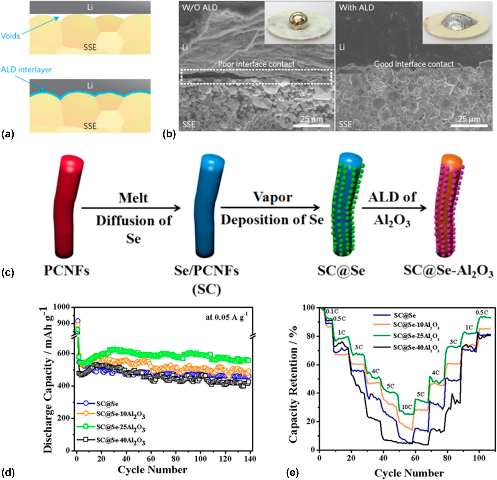
To improve the comprehensive performance of the batteries, commonly a well-designed structure is needed. ALD is capable to construct an intermediate layer or auxiliary medium for the nanostructure engineering of the entire battery system including the anode, the cathode, the electrolyte, the separator, and especially the interfaces between them. For instance, the giant interfacial impedance of lithium/garnet-type electrolyte in garnet-type solid-state electrolyte Li batteries had block the development of this environment stable, efficient, and promising storage devices for a long time. Hu et al. [Reference Han, Gong, Fu, He, Hitz, Dai, Pearse, Liu, Wang, Rubloff, Mo, Thangadurai, Wachsman and Hu103] found that the ultrathin Al2O3 membrane could effectively negate the interfacial impedance between the metal lithium and the garnet electrolyte for its decreased sintering temperature and increased lithium ion conductivity. As shown in Figs. 2(a) and 2(b), they modified the garnet surface with 40 ALD cycles of Al2O3 coating [Reference Wolfenstine, Allen, Read and Sakamoto104]. They found that the Al2O3 layer could help the molten Li conformally to coat the surface without void space, which can be distinctly observed in the SEM images in Fig. 3(b) that the Al2O3 layer enhances the contact between the garnet and the metal Li. The impedance of the obtained ALD-modified interfacial layer showed a relatively low value of 1 Ω cm2 compared with 1710 Ω cm2 of the non-ALD samples at room temperature. They ascribed the improvement of the performance to the wetting of metal lithium in contact with the garnet electrolyte and the efficacious lithium ion transport through the interfacial layer offered by the ALD Al2O3. Another case is that the atomic layer Al2O3 was utilized to construct stable freestanding carbon–selenium cathodes which exhibited a high mass loading of selenium as well as superior cyclic performance.
(a) Schematic of the wetting behavior of garnet surface with molten Li. (b) SEM images of the garnet solid-state electrolyte/Li metal interface. Without the ALD-Al2O3 coating, garnet has a poor interfacial contact with Li metal even on heating. With the help of ALD–Al2O3 coating on garnet, Li metal can uniformly bond with garnet at the interface on heating. Inset are photos of melted Li metal on top of the garnet surface clearly demonstrating classical wetting behavior for the ALD-treated garnet surface. (a) and (b) are adapted from Ref. Reference Wolfenstine, Allen, Read and Sakamoto104. (c) Schematic illustration of the preparation process for SC@Se–xAl2O3 composites. (d) Cycle stability of SC@Se–xAl2O3 composites. (e) Comparison of the rate capability of SC@Se–xAl2O3 composites expressed as a percentage of the initial capacity at 0.1 C. (c)–(e) are adapted from Ref. Reference Ma, Li, Yang, Mi, Luo, Deng, Yan, Zhang, Lin, Ren, Li and Zhang102.
(a) Schematic illustration of the NG/S–TiO2 preparation process and the experimental demonstration showing that the battery can light up two blue LEDs. (b) The rate performances of the electrodes at various current densities. (a) and (b) are adapted from Ref. Reference Yu, Ma, Song, Wang, Tian, Wang, Qiua and Wang109. Characterization of as-prepared HF-etched Ti3C2 MXene: (c) XRD patterns of Ti3AlC2 and Ti3C2. (d) Typical SEM image of HF-etched Ti3C2 Mxene. TEM analysis of MXene sheets coated with a 50 nm-thick layer of SnO2: low-magnification TEM image and SAED pattern for ALD (e) at 150 °C and (f) at 200 °C. (g) Fourier-filtered high-resolution RGB image for ALD at 200 °C, showing the presence of two phases and (h) STEM image along with the EDS line-scan for ALD @150 °C showing the conformal SnO2 coating. (c)–(h) are adapted from Ref. Reference Ahmed, Anjum, Gogotsi and Alshareef110.

Zhang and his coworkers fabricated a selenium composite cathode material by vapor depositing Se onto porous carbon nanofiber mats and subsequently ALD of Al2O3 with the synthesis routine shown in Fig. 2(c) [Reference Ma, Li, Yang, Mi, Luo, Deng, Yan, Zhang, Lin, Ren, Li and Zhang102]. They firstly introduced the ALD technique into the Se batteries and systematically investigated the effect to the electrochemical properties of the batteries induced from the Al2O3 thickness that is precisely controlled by the ALD. A 67 wt% of Se content correspondingly provided by 25 cycles Al2O3 layers shows an excellent cyclic stability which can deliver specific capacity of 503.5 mA h/g after 1000 cycles at 0.5 A/g and even maintain 72.1% of the capacity comparing to the original with analysis details shown in Figs. 2(d) and 2(e). They contributed the enhancement of the performance to the exceptional conductivity, fast ionic/charge transfer, limitation of the dissolution of the sodium polyselenides, and the confinement of the volume expansion during charging/discharging.
Moreover, Hwang et al. [Reference Hy, Chen, Cheng, Pan, Cheng, Rick and Hwang105] build a flexible connection via the combination of ALD Al2O3 between the Si anode and the additive vinylene carbonate (VC), which remarkably led to an increasement of performance from a 73 to 11% capacity loss. Additionally, some other materials such as titanium oxide (TiO2), tin oxide (SnO2), and even the garnet Li7La3Zr2O12 (LLZO) also have been deposited to optimize the lithium batteries performance serving as a structure modification layer [Reference Kazyak, Chen, Wood, Davis, Thompson, Bielinski, Sanchez, Wang, Wang, Sakamoto and Dasgupta106, Reference Guan, Li, Yu, Mao, Wong, Yanc and Wang107, Reference Jiang, Luo, Zhu, Huang, Liu and Yu108].
ALD for active electrode materials
Direct implementation of ALD on the synthesis of electrode materials may also provide an insight to the design of novel batteries. Because of the great capability to form conformal and thickness-controlled membranes, ALD emerges as an ideal technique to fabricate anode or cathode materials that can basically determine the specific capacity, durability, and other electrochemical performance of the batteries. A typical example is that Wang and coworkers fabricated a sandwich-like structure media as a cathode for Li–S battery using N-doped graphene (NG), sulfur, and ALD–TiO2 as raw materials [Reference Yu, Ma, Song, Wang, Tian, Wang, Qiua and Wang109]. As the details shown in Fig. 3(a), TiO2 was deposited on the NG-pure sulfur composites that are used as a conductive matrix and the source of elemental S. Two LED bulbs can even be lightened by the assembled battery using the composite as raw materials. Various cycles of ALD here for 0, 50, 20, and 40 were adopted to investigate the effect of the ALD thickness to the performance. The obtained hybrid active material showed robust and steady architectures, which induced to the great improvement of the results as the NG/S–20TiO2 could deliver 1374 mA h/g at 0.1 C for discharge capacity and keep an average coulombic capacity efficiency of approximately 99.7% at 1 C [see in Fig. 3(b)]. Ahmed et al. [Reference Ahmed, Anjum, Gogotsi and Alshareef110] proposed a methodology that oxide anodes can be grown on two-dimensional titanium carbide sheets (MXenes) through the ALD [XRD patterns, SEM, and TEM images shown in Figs. 3(c)–3(h)]. They deposited atomic layered SnO2 up to the MXene, which showed an excellent electrochemical performance working as anodes for LIBs. Similarly, some other recent works on ALD SnO2 were also studied by using various conductive substrates such as graphene nanosheets and carbon nanotubes for electrodes of batteries [Reference Xie, Sun, George, Zhou, Lian and Zhou111]. In summary, ALD has provided a good venue to build ideal electrode materials with excellent inner electrochemical performance and external controllable physical properties. However, most of the anode or cathode materials still suffer the deterioration during working process which has attracted the attention of the researchers.
Recently, Zhao and coworkers made a multilayer structure comprising two porous C layers and one sandwiched active ZnO (CZC) nanosheet [Reference Zhao, Huang, Wang, Ma, Fan, Bao and Mei79], and the fabrication details and the corresponding characterizations are presented in Figs. 4(a)–4(d). In this composite, the thickness of the interlayer zinc oxide was accurately controlled by the ALD, which was used to investigate the effect of the thickness between the ZnO and the carbon coating. They found that the battery could perform a high capacity of 300 mA h/g at 5000 mA/g with the ratio of ZnO/C at about 1:1. The critical thickness ratio was proposed because the carbon layer is found fragile when the interlayer is thicker than the critical value which may ruin the stable SEI layer and reduce the conductivity. Additionally, ALD ZnO was also fabricated on expanded graphite (EG) as a binder-free anode for LIBs by Li and his coworkers [Reference Li, Zhao, Huang, Xu, Wang, Pan, Men and Mei112] with the details shown in Figs. 4(e)–4(h). The composite was pressed into both self-supporting and flexible film and thus was directly utilized as anode. The ALD-ZnO/expanded graphite (ZG) anode battery shows a high stable capacity without using any conductive agent, binder, and current collector.
(a) Schematic of the synthesis procedure of CZC nanosheets. SEM images demonstrating the change of the electrode structure before and after 200 discharge/charge cycles. (b) Cross-sectional TEM image of a CZC nanosheet. The nanosheet is composed of a sandwiched structure. (c) High-resolution TEM image of the C/ZnO interface. (d) Nitrogen adsorption–desorption isotherms and pore size distribution (inset) of the CZC nanosheet sample. (a)–(d) are adapted from Ref. Reference Zhao, Huang, Wang, Ma, Fan, Bao and Mei79. (e) Schematic diagram of ZG preparation and corresponding device assembling. (f) CV curves of anode made from ZG300 (first three cycles) at 0.2 mV/s. The inset shows corresponding CV results from pure ZnO anode for comparison. (g) The 1st, 2nd, 5th, and 10th discharge and charge curves of ZG300 and pure ZnO (inset) at a current rate of 200 mA/g; (h) EIS of anode made from EG and ZG composites before galvanostatic discharging/charging cycles. The inset shows the equivalent circuit used to fit the experimental results. (e)–(h) are adapted from Ref. Reference Li, Zhao, Huang, Xu, Wang, Pan, Men and Mei112.

ALD for the passivation layer
There is a well-known challenge that the dissolution or the side reactions of the active electrode materials in the electrolyte could seriously affect the cycling performance of the batteries [Reference Goodenough and Kim113]. One aspect to ameliorate the situation we discuss here is the achievement which has been obtained by constructing an ALD passivation/protection layer onto the active materials. One typical example is that Alexander and his coworkers proved that ALD Al2O3 can effectively protect the Li metal from corrosion [Reference Kozen, Lin, Pearse, Schroeder, Han, Hu, Lee, Rubloff and Noked57]. The electrode was used as an anode for Li–S batteries to investigate the function of the ALD coating and they found that 14 nm ALD Al2O3 could alleviate the first cycle capacity loss because the ALD layer protected metal anode from the erosion of both the sulfur species and the electrolyte [see Fig. 5(a)]. As exhibited in Fig. 5(b), the great electrochemical performance with a 14-nm ALD Al2O3 coating can be clearly observed. Recently, Zhang’s group used ALD TiO2 to protect the flexible C/S/BaTiO3 electrode (CSB@TiO2) for room temperature Na–S batteries which also provide a novel case for the ALD passivation layer on batteries [Reference Ma, Li, Yang, Mi, Luo, Deng, Yan, Rauf, Zhang, Sun, Ren, Li and Zhang114]. In the work, they developed a tactic to synthesize a hybrid consisted of porous freestanding C mats, 3 wt% ferroelectric BaTiO3 nanoparticles, and thickness-controlled TiO2 [see Fig. 5(c)]. Corresponding TEM images and digital photos are shown in Fig. 5(d), respectively. They found that the ALD-modified electrode exhibited an excellent durability of remaining 382 mA h/g after 3000 cycles with a coulombic efficiency of 106.1% based on the 2nd cycle at 2 A/g. It is concluded that the function of TiO2 passivation layer could inhibit the volume extension, capture and limit the intermediate polysulfide inside the conductive matrix, and keep the ionic transfer interface stable, which led to the high performance of the Na–S batteries. Yu et al. [Reference Yu, Wang, Tian, Song, Wang, Li, Hongd and Shi115] fabricated a graphene–sulfur composite with dual-protection by a compact graphene skin and ALD oxide coating for LSBs [see sample photos in Fig. 5(e)]. The enhanced performance can be ascribed to the preservation of the lithium polysulfide intermediates by the synergistic function of the graphene and the ALD-coated layer, which can enhance the structural stability.
(a) Optical analysis of lithium foil surface tarnishing during atmospheric exposure at 25 °C and 40% relative humidity. (α) unprotected and (β) 14 nm ALD Al2O3-protected Li metal foil immediately upon removal from an argon atmosphere (γ) Bare and (δ) 14 nm ALD Al2O3-protected Li metal foil after 20 h exposed to atmosphere at 25 °C and 40% relative humidity. (b) anode protected with 14 nm ALD Al2O3 LiS cells. (a)–(e) are adapted from Ref. Reference Kozen, Lin, Pearse, Schroeder, Han, Hu, Lee, Rubloff and Noked57. (c) Schematic illustration of the CSB@TiO2 electrode preparation process. (d) TEM images of the CSB@TiO2 nanofiber and photograph of the CSB@TiO2 freestanding electrode. (c) and (d) are adapted from Ref. Reference Ma, Li, Yang, Mi, Luo, Deng, Yan, Rauf, Zhang, Sun, Ren, Li and Zhang114. (e) Digital images of GO–S dispersion, as-obtained G–S hydrogel and a bent G–S aerogel. Scale bars, 1 cm. Adapted from Ref. Reference Yu, Wang, Tian, Song, Wang, Li, Hongd and Shi115.

Applications of ALD in supercapacitors
Supercapacitors as a new-generation energy storage system hold excellent performance such as high power density, fast charge/discharge rate, and good cycling performance [Reference Zhao, Liu, Zhu, Xu, Li, Huang, Zhang and Liu1, Reference Zhu, Murali, Stoller, Ganesh, Cai, Ferreira, Pirkle, Wallace, Cychosz, Thommes, Su, Stach and Ruoff116, Reference Snook, Kao and Best117, Reference Simon and Gogotsi118, Reference Pandolfo and Hollenkamp119]. Supercapacitors are typically classified into electric double-layer capacitors (EDLCs) and pseudocapacitors. The mechanism of EDLCs can be attributed to electrostatic charge diffusion and accumulation at the interface of the electrode/electrolyte, whereas pseudocapacitors deliver high capacitance by Faradaic reactions at the electrode materials [Reference Wei, Sevilla, Fuertes, Mokaya and Yushin120, Reference Chen, Qiu, Ren, Guan, Lin, Zhang, Chen, Wang and Peng121, Reference Bose, Kuila, Mishra, Rajasekar, Kim and Lee122]. The pseudocapacitors could deliver more attractive values of energy density than EDLCs [Reference Sruthi and Kartick123, Reference Liu and Pan124, Reference Feng, Li, Yang and Huang125, Reference Fan, Ren, Yang, Yu and Wang126].
Among various materials, transition metal oxides are viewed as an ideal electrode material for pseudocapacitors. Aimed to depositing active materials via ALD, Guan et al. [Reference Guan, Qian, Wang, Cao, Zhang, Li and Wang127] deposited Co3O4 nanolayers on a flexible carbon nanotubes/carbon cloth (CC) substrate by ALD [Fig. 6(a)]. The highest capacitances obtained for the CNT@2400–Co3O4/CC is 416.7 mF/cm2 and the improvement can be attributed to the mechanically robust CC/CNTs substrate [Fig. 6(b)], the uniform coated high capacitance materials of Co3O4 nanoparticles, and the unique hierarchical structure. Parsons et al. [Reference Daubert, Lewis, Gotsch, Mundy, Monroe, Dickey, Losego and Parsons128] grew V2O5 thin films via ALD process on active carbon powders to form meso- and microporous carbon electrodes. As shown in Fig. 6(c), V2O5 ALD near the pore opening would block the pores, thus decreasing double layer capacitance. In addition, the V2O5 increased pseudocapacitance but decreased the accessible pores and double layer capacitance, leading to only a minimal change in overall capacitance at low ALD cycles. Also, the cyclic voltammetry scans for the ALD-coated carbon powders were less rectangular. A thicker V2O5 layer can increase total charge capacity, whereas a thinner V2O5 layer required shorter charge diffusion times, thus enabling quicker faradaic charge storage. Figure 6(d) demonstrates the great electrochemical performance in terms of large specific capacitance and good rate performance.
(a) The morphology and electrochemical performance of Co3O4 nanolayers on a flexible CC, (b) capacitance at various current densities of as-obtained composites. (a) and (b) are adapted from Ref. Reference Guan, Qian, Wang, Cao, Zhang, Li and Wang127. (c) Schematic image of V2O5 thin films via ALD process on active carbon powders. (d) Specific capacitance at various scan rates, (c) and (d) are adapted from Ref. Reference Daubert, Lewis, Gotsch, Mundy, Monroe, Dickey, Losego and Parsons128. (e) and (g) SEM images of uncoated CNT and smooth nanostructured vanadium oxide coatings on the surface of multiwalled carbon nanotube. (f) and (h) Charge discharge curves of as-obtained materials. (e)–(h) are adapted from Ref. Reference Boukhalfa, Evanoff and Yushin37.

Boukhalfa et al. [Reference Boukhalfa, Evanoff and Yushin37] designed a structure-allowed uniform deposition of smooth nanostructured vanadium oxide coatings on the surface of multiwalled carbon nanotube (CNT) electrodes, thus offering a novel route for the formation of binder-free flexible composite electrode fabric for supercapacitor applications with greatly improved electrical conductivity and cycle stability [Figs. 6(e) and 6(g)]. As shown in Figs. 6(f) and 6(h), the electrochemical performance of capacitance largely enhanced by ALD vanadium oxide coating. With 100 ALD cycles, the composites exhibit pseudocapacitance.
Sun et al. [Reference Sun, Xie, Wang, Sun, Cavanagh, Travis, George and Lian35] fabricated a nanoscaled coating of titanium oxide on graphene via a novel atomic ALD approach. The TiO2 nanoparticles formed by ALD are homogeneously anchored onto the porous graphene sheets. The strong chemical bonding resulting from ALD ensures excellent electrical conductivity and stability throughout the entire three-dimensional network. In addition, TiO2 provides pseudocapacitance and further enhanced the electrochemical performance. Figures 7(a)–7(d) show the SEM images of titanium oxide coatings on graphene, and Fig. 7(e) demonstrated the electrochemical performance in capacitance, which exhibits large capacitance and good rate capability. As a potential supercapacitor material, the composites exhibited a capacity of 75 F/g and 84 F/g at a scan rate of 10 mV/s for composites grown using 50 and 100 ALD cycles, respectively. The nearly identical Nyquist plots of the TiO2–G composites compared with those of pure graphene demonstrated that the composites possess excellent conductivity for charge transfer and open structures for ion diffusion. Aimed to titanium oxide coatings through ALD technique, we recently fabricated TiO2 nanomembranes with different thicknesses via ALD technique and used them for supercapacitor [Figs. 7(f)–7(i)] [Reference Naeem, Naeem, Zhao, Wang, Zhang, Mei and Huang80]. The uniform TiO2 nanomembrane enhances the capacitance up to 2332 F/g at 1 A/g [Fig. 7(j)].
(a)–(d) SEM images of TiO2–G composite grown different ALD cycles. (e) Specific capacitance at various scan rates. (a)–(e) are adapted from Ref. Reference Sun, Xie, Wang, Sun, Cavanagh, Travis, George and Lian35. (f)–(i) Fabrication process and morphologies of TiO2 nanomembranes with different thicknesses. (f) Sketch represented fabrication process of TiO2 nanomembranes. (g)–(i) SEM images of TiO2 nanomembranes with 100, 200, and 400 ALD cycles, respectively. (j) Specific capacitance at various current densities. (f)–(j) are adapted from Ref. Reference Naeem, Naeem, Zhao, Wang, Zhang, Mei and Huang80.

Applications of ALD in biosensors
Sensors have important applications among society. They are widely applied to industrial emission monitor, biomedical, and agricultural related fields [Reference Ripka and Janosek129, Reference Lee, Roh and Park130, Reference Hill, Vijayaragahvan and Novoselov131, Reference Han, Peng, Sun, Venkatesh, Chung, Lau, Zhou and Roy132]. Thanks to its excellent performance in thickness and composition control, as well as the conformallity; ALD can be applied in the preparation of various kinds of sensor devices [Reference Zhang, Zhang, Yao, Xia and Chen133, Reference Chikae, Fukuda, Kerman, Idegami, Miura and Tamiya134].
For directly depositing high catalytic active materials, Chio et al. [Reference Choi, Kim, Lee, Kim, Choi, Kim, Kim, Park and Kim135] synthesized CNTs decorated with Ni by ALD [Fig. 8(a)]. The CNT-Ni composites exhibited high electrocatalytic activity for glucose oxidation in alkaline solutions. ALD can help Ni particles to be well deposited on CNTs, and this controllable construction led to an enhanced detection performance, such as high sensitivity, rapid response, wide linear response window, good selectivity, and repeatability for nonenzymatic detection. As shown in Fig. 8(b), CNT-Ni exhibits high sensitivity to target glucose and good selectivity. On the other hand, Yang et al. [Reference Yang, Tong, Wang, Gao, Guo and Qin78] used ALD to deposit NiO nanoparticles on SiC particles. The TEM images of composites were shown in Fig. 8(c). Taking advantages of ALD process, the NiO particles uniformly grew on SiC. As shown in Fig. 8(d), the NiO/SiC exhibits advantages of high glucose-sensing ability, low detection limit, high sensitivity, wide linear detection range, and good stability. The NiO/SiC prepared with 600 ALD cycles of NiO had the best sensing performance among the 200-, 400-, 600-, and 800-NiO/SiC with a sensitivity of 2.037 mA/(mM/cm2). Zhang et al. [Reference Zhang, Huang, Qian, Yuan, Wang and Chen136] created a flexible electrode by depositing an ultrathin CoO layer on the skeleton surfaces of a nanoporous gold film by ALD [Fig. 8(e)]. The hybrid showed high catalytic activity for glucose oxidation and H2O2 reduction due to the excellent synergistic performances of interfacial Au and CoO, as well as the gold skeleton with a large surface area. Because of high catalytic performance of the CoO layer, as shown in Fig. 8(f), the composites exhibit good sensitivity to target samples.
(a) SEM image of CNT–Ni composites. (b) Amperometric responses of the CNT–Ni–GCE with constant stirring in 0.1 M NaOH after successive glucose additions at V a of +0.50 V. Inset: the amperometric response to 2 and 5 μM. (a) and (b) are adapted from Ref. Reference Choi, Kim, Lee, Kim, Choi, Kim, Kim, Park and Kim135. (c) TEM images of NiO/SiC composites. (d) CV curves of NiO/SiC with different ALD cycles in 1 M KOH solution at a scan rate of 50 mV/s. (c) and (d) are adapted from Ref. Reference Yang, Tong, Wang, Gao, Guo and Qin78. (e) SEM image of NPG films after CoO deposition with various ALD cycles. (f) CV curves of the NPG/CoO electrode in 0.5 m KOH solution with different amounts of glucose at a scan rate of 20 mV/s. (e) and (f) are adapted from Ref. Reference Zhang, Huang, Qian, Yuan, Wang and Chen136. (g) TEM image of CF@CuAl-LDH. (h) Dose–response curve for glucose detection. (g) and (h) are adapted from Ref. Reference Wu, Wan, Shi, He, Xu, Tang, Hao and Wang137.

In addition, the ALD coatings as precursor and seed can take part in chemical reaction to form active materials. Recently, Wu et al. [Reference Wu, Wan, Shi, He, Xu, Tang, Hao and Wang137] used ALD to form uniform Al2O3 coating on carbon fiber to induce the growth of layered double hydroxide (LDH), and a carbon fiber-supported ultrathin CuAl LDH nanosheets (CF@CuAl-LDH) was obtained. The TEM image of CF@CuAl-LDH is shown in Fig. 8(g). In their work, Al2O3 was deposited by ALD at a deposition temperature of 150 °C. As shown in Fig. 8(h), the CF@CuAl-LDH had an excellent intrinsic peroxidase mimic activity for peroxidase substrate 3,3′,5,5′-tetramethylbenzidine (TMB), thus providing a rapid, sensitive, and selective colorimetric method for sensing glucose.
Because of good biocompatibility, ALD-prepared membrane can be used as transducer to load bioactive molecule. Utilizing this method, Tereshchenko et al. [Reference Tereshchenko, Fedorenko, Smyntyna, Konup, Konup, Eriksson, Yakimova, Ramanavicius, Balme and Bechelany84] reported their optical biosensor aimed for the determination of Grapevine virus A-type (GVA) proteins (GVA-antigens) based on ALD ZnO films. The GVA-antigen detection was performed by using the changes in the GVA-related light emission. The sensitivity of the biosensor was tested to be in the range from 1 pg/mL to 10 ng/mL of protein. Dominik et al. [Reference Dominik, Lesniewski, Janczuk, Niedziolka-Joensson, Holdynski, Wachnicki, Godlewski, Bock and Smietana85] deposited titanium oxide thin films on a long-period grating (LPG) induced in an optical fiber for the recognition of the complex formation between biotin and avidin. The sensitivity of the sensor was close to 3400 nm/RIU for LPG. Here, titanium oxide coating plays a role in modifying the sensor sensitivity, as well as enabling biofunctionalization and recovering process of the surface.
The uniform wrapping of thin films can provide great protection for whole device from harsh environment. Jeon et al. [Reference Cha, Lee, Jordan, Lee, Oh, Kim, Park, Hong and Jeon138] reported a unique structure where SiO2 films with a thickness of few nanometers were deposited on susceptible In–P wafer, which protected the underlying In–P from extremely harsh environments. Schematic surface functionalization steps for biosensing tests are shown in Fig. 9(a). Then, with the biotinylation of ALD-SiO2 surface, chemical interaction between biotin and streptavidin molecules tagged with phosphor (SAPE) allows the detection. As demonstrated in Figs. 9(b) and 9(c), the device decorated with ALD thin film is able to detect streptavidin with a large refractive index sensitivity of ∼163 nm/RIU, and, meanwhile, generates a figure of merit of ∼800. Flandre et al. [Reference Couniot, Vanzieleghem, Rasson, Van Overstraeten-Schloegel, Poncelet, Mahillon, Francis and Flandre82] developed a novel structure for direct and selective detection of bacteria via lytic enzyme. The schematic for its function mechanism is demonstrated in Figs. 9(d) and 9(e). A CMOS-compatible chip was coated with a thin layer of ALD Al2O3 in average thickness of 30 nm. As the PDMS cap is pressed on the device, the whole microfluidic channel is formed [Fig. 9(d)]. The incubation of lytic enzyme was able to function with target bacteria in the matrix flow, thus accomplish the whole bacteria detection. The Al2O3 layer protected the chip from corrosion of electrolyte and reduced the detrimental effects on bacterial sensitivity. As shown in Fig. 9(e), because of the protection of ALD Al2O3, the sensors exhibited an outstanding detection limit of approximately 108 (CFU/mL) min in a 1.5 μL microfluidic chamber with an additional setup time of 50 min.
(a) Schematic surface functionalization steps for biosensing test. Graphs show the lasing spectra of the biosensors in (b) dipole-like Γ2 BEL mode and (c) monopole-like Γ1 BEL mode. Spectra in each plot are vertically shifted for clarity. (a)–(c) are adapted from Ref. Reference Cha, Lee, Jordan, Lee, Oh, Kim, Park, Hong and Jeon138. (d) and (e) The illustration of sensing events: (I) washing with PBS 1:1000, (II) incubating 5 × 10⁸ CFU/mL E. faecium in synthetic urine, (III) incubating 5 × 10⁸ CFU/mL S. epidermidis in synthetic urine and (IV) incubating lysostaphin. Shifts after wash Δ1, Δ2, and Δ3 are evaluated after the addition of E. faecium, S. epidermidis, and lytic enzymes, respectively. (d) and (e) are adapted from Ref. Reference Couniot, Vanzieleghem, Rasson, Van Overstraeten-Schloegel, Poncelet, Mahillon, Francis and Flandre82. (f) Schematic illustration of uniform ALD coating on a single conical nanochannel. (g) Example of current trace seen before and after adding buffered 100 nM BSA solution to the tip side of the conical nanochannel. (f) and (g) are adapted from Ref. Reference Wang, Fu, Wang, Kong, Sheng, Wang, Chen and Xue139. (h) and (i) The schematic image and SEM micrograph of a freestanding region of TiO2 waveguide. (h) and (i) are adapted from Ref. Reference Purniawan, Pandraud, Moh, Marthen, Vakalopoulos, French and Sarro92.

Because of the stability of films based on ALD, the protective shell made from ALD technique broadens the application in regenerated biosensors. Xue et al. [Reference Wang, Fu, Wang, Kong, Sheng, Wang, Chen and Xue139] designed a conical nanochannel for protein sensing. The unique structure was built by track-etching and then modified via ALD Al2O3. With the conformal depositing, Al2O3 thin film coated on the surface uniformly and constructed resultant nanochannels [Fig. 9(f)]. The conical nanochannels can hinder the travel rate of bovine serum albumin to enhance the capture rate with excellent signal-to-noise ratio for the transport events [Fig. 9(g)]. Purniawan et al. [Reference Purniawan, French, Pandraud and Sarro140] developed a freestanding structure of rib via ALD-deposited TiO2 [Figs. 9(h) and 9(i)], which was selective to Escherichia coli, and used the structure to sense its presence. The sensitivity, evaluated by evaporation of several concentrations of ethanol and isopropyl alcohol diluted in water, was found to be 0.85 and 1.34 dB/% (v/v), respectively.
It is worth noting that some nanoarchitectures fabricated by ALD have similar dimensions with the biological components of the biorecognition film, and therefore draw considerable attention. Comstock et al. [Reference Comstock, Christensen, Elam, Pellin and Hersam141] produced rough Pt films via template-assisted ALD coating, as characterized by roughness factors as large as 310. The nanostructured Pt film was applied in enzyme-free glucose sensing and displayed a desirable near-linear response to glucose in the range of 0–20 m M with a sensitivity of 63.8 μA/(cm2/mM).
Applications of ALD in other sensors
Gas sensors are widely used in industrial emission monitor and environment protection field. ALD technique has also been extensively applied. Du et al. [Reference Du and George142] prepared ultrathin SnOx films by ALD and the SnOx films can be served as a CO gas sensor, of which maximum response for CO gas sensing was observed at a SnOx film with a thickness of 26.2 Å. The pictures of the front and back sides of the hotplate template are shown in Fig. 10(a). The response of gas sensor was temperature dependent and displayed its highest responsivity at temperatures between 250 and 325 °C. Sensor response for a CO pressure of 11 m torr at 300 °C for different SnOx ALD film thicknesses grown on separate hotplate templates is shown in Fig. 10(b). Niskanen et al. [Reference Niskanen, Varpula, Utriainen, Natarajan, Cameron, Novikov, Airaksinen, Sinkkonen and Franssila143] used ALD to produce gas-sensitive tin dioxide film in a microhotplate gas sensor. Ethanol, acetone, and acrylonitrile were used as model analytes to investigate the device performance. The results demonstrated good response, low drift rates of the output signal, and good operational stability in the short term.
(a) Pictures of the front and back sides of the hotplate template. (b) Sensor response for a CO pressure of 11 m torr at 300 °C for different thicknesses of ALD SnOx films thicknesses. (a) and (b) are adapted from Ref. Reference Du and George142. (c) Schematic of 1D p-CuO/n-ZnO hollow nanofibers synthesis using a three-step method. (d) Responses of the 0.3 (g) CuO/ZnO200 (cycles), 0.3 (g) CuO/ZnO400 (cycles), and 0.3 (g) CuO/ZnO600 (cycles) HNFs sensors. (e) Dynamic resistance changes of 0.3CuO/ZnO600 HNFs sensor exposed to 100 ppm H2S as a function of operating temperature. (c)–(e) are adapted from Ref. Reference Han, Li, Shao, Li, Ma, Zhang and Liu145. (f) SEM images of ZnO nanosheet on sponge and freestanding ZnO nanosheet. (g) Responsivity varying with the voltage under different irradiated power densities. (f)–(g) are adapted from Ref. Reference Guo, Zhao, Wang, Chen, Zhao, Jiang, Huang, Di and Mei149.

Yun et al. [Reference Yun, Seo, Lee and Yoon144] reported NH3 gas sensors with semiconductor thin-film transistor (TFT) configuration using ALD ZnO nanoparticles as gas-sensing element. Oxygen molecules on the surface of exposed sensing materials in atmosphere extract the electrons from the conduction band in ZnO nanoparticles to form oxygen ions when thermal energy is supplied, and when contacted with NH3 gas, by-products such as NH4OH were generated and the conductivity changes can be observed by measuring drain current (I DS) of TFT. The device showed high sensitivity to target gas, excellent retrievability after the gas removal, and stable device performance even after the repeated measurements.
On the other hand, Han et al. [Reference Han, Li, Shao, Li, Ma, Zhang and Liu145] reported the fabrication of 1D p-CuO/n-ZnO hollow nanofibers with high detection performance for H2S by the combination of electrospinning and ALD technique [Fig. 10(c)]. Taking advantages of ALD, the ratios of Zn to Cu (R Zn/Cu) was controlled, which optimized the repeated gas-sensing performance. The optimum response of these materials was improved about 6-fold versus the neat ZnO and 45-fold versus neat CuO. Meanwhile, an improvement in the selectivity and stability of these H2S sensors was also observed [Figs. 10(d) and 10(e)].
In addition, ALD can also take part in the fabrication of pH sensors. Lin et al. [Reference Lin, Huang, Chow, Lan, Yang, Chang and Lai146] reported an light-immune pH sensor with a SiC-based electrolyte-insulator-semiconductor structure, which overcame the problem caused by light penetration. 10 nm ALD HfO2 was deposited on the supporting wafer. This device reached an average pH sensitivity of 52.35 mV/pH and had a low light response (3.9–8.6 mV) due to its intrinsic property of having a wide band gap. Jakob et al. [Reference Jakob, Gutsch, Chatelle, Krishnaraja, Fahlteich, Weber and Zacharias147] used low-temperature ALD to fabricate ZnO and Al2O3 thin films for pH sensor. The Al2O3 thin film was applied as a sensitive layer on the ZnO thin film, and meanwhile acted as a gate oxide between the liquid gate potential and the ZnO channel. This small volume potentiometric pH sensor based on flexible and transparent field effect transistors had a good pH sensitivity for wide pH ranging from 5 to 10. Recently, Wang et al. [Reference Wang, Li, Zhang, Liu and Ao148] enhanced the pH sensitivity of AlGaN/GaN ion-sensitive field-effect transistor (ISFET) by coating an ALD Al2O3 layer on its sensing area. The Al2O3 coating not only successfully reduced the surface state density and the current in the solution but also induced higher density of sensing site as well as better surface hydrophilicity, leading to an improved sensitivity of 57.8 mV/pH for the Al2O3-ISFET. Recently, Guo et al. [Reference Guo, Zhao, Wang, Chen, Zhao, Jiang, Huang, Di and Mei149] developed a simple and convenient approach to synthesize large amounts of ZnO nanosheets [Fig. 10(f)], which are suitable for producing the key component of printed ultraviolet photodetectors. As shown in Fig. 10(g), the obtained printed ultraviolet photodetector that utilizes ZnO nanosheets as the functional materials exhibits a high responsivity of ∼148 A/W and a response time of 19 s.
Summary and outlook
In the past decade, ALD has undergone tremendous progress and become an efficient technique for nanostructures fabrication. In many studies, ALD was proven to be valuable because of its ability to improve device performance. Thanks to its ability to fabricate advanced nanostructures and generate uniform coatings on the surface, ALD has become one of the most promising deposition methods and is used in a variety of applications.
The films deposited by ALD are of extremely high quality and precise thickness and composition control, while also providing a high degree of uniformity, which is a significant capability in the fabrication of novel nanostructures. Therefore, ALD is widely used for active material growth and deposition, formation of protective layers, and direct establishment of nanostructures. These aspects are well represented in applications like supercapacitors, batteries, and sensors. For batteries, ALD can be applied to structure engineering/modification layer formation for better performance. The active electrode materials for excellent electrochemical performance and controllable physical properties, as well as passivation layer to get electrodes free from the threats from the working environment, were fabricated and investigated. In addition, good biocompatibility makes ALD work well in biosensors and can be used for the sensing of glucose (both enzyme detection and enzyme-free detection), protein, etc. Other types of sensors are also becoming more sensitive because of ALD, including but not limited to some gas sensors and pH sensors.
However, there is still a long way to go before ALD comes to scale application. ALD now remains a relatively slow method than other conventional deposition methods. To solve this problem, many enhancements, e.g., plasma, which can lower the reaction temperature and accelerate the reaction rate, have been induced to the system. Based on the advantages of ALD technology itself and existing researches, we can say with certainty that ALD will still be in a rapid development stage. We believe it will be more commonly used in energy storage applications and sensor devices as well as many other fields. With the increasing emphasis on this field and the development of ALD technology itself, the large-scale application of ALD-based nanostructures will make this technology more affordable in the future.
Acknowledgments
This work was supported by the Natural Science Foundation of China (Nos. 61975035 and U1632115), Science and Technology Commission of Shanghai Municipality (No. 17JC1401700), the National Key R&D Program of China (Nos. 2017YFE0112000 and 2015ZX02102-003), and the Program of Shanghai Academic Research Leader (19XD1400600).


