


I. INTRODUCTION
The processing speed of microprocessors is continuously increasing due to the significant progress in down-scaling transistor size [Reference Moore1, 2]. This advancement results in the production of fast and dense complementary metal oxide semiconductor (CMOS) chips which pose a challenge for on-chip and chip-to-chip interconnects due to smaller real estate available to metal wires [Reference Lopez, Murali, Sarvari, Bowman, Davis and Meindl3–Reference Balamurugan6]. Hence, novel interconnection methods are essential in order to provide links with high bandwidth, low latency, and low power consumption. To tackle this issue, optical links are broadly investigated in order to assess their feasibility for short reach (i.e., few millimeters to several centimeters) interconnection [Reference Young7–Reference Dai and Bowers10].
Recently, we have introduced and successfully demonstrated a novel hybrid finite ground coplanar waveguide (FGCPW) interconnect structure which supports high-speed signal transmission at microwave and optical frequencies, simultaneously [Reference Banan, Hai, Berini and Liboiron-Ladouceur11]. The proposed FGCPW structure consists of two thin ground strips of 25 nm thickness and a 1 µm thick signal strip. This approach provides a new paradigm for short reach communications where high-frequency electrical and optical signals co-exist on the same structure. This leads to reduced number of layers (i.e., less complexity) and also a potentially increased bandwidth density of the metal wires. The envisioned application for the discussed hybrid link is in architectures where an electrical interface between chips is implemented using ball-grid arrays (BGAs) or micro bumps. The proposed structure has inherently unlimited bandwidth density because it supports optical signal. Optical bandwidth limitations originate from E/O and O/E converters bandwidth. The goal of this structure is to provide efficient and low energy consumption chip-to-chip interconnects (several mm to few cm long links) by allocating high data rate channels to the optical section and sending lower data rates (e.g., control signals or low-speed data) over electrical section.
Measurement results of the hybrid link [Reference Banan, Hai, Berini and Liboiron-Ladouceur11] shows simultaneous error-free transmission (BER <10−9) of optical and electrical data at 40 and 12 Gbps, respectively, over a 3 mm long structure without any observable interference. The measured channel losses for the optical and electrical signals are approximately 12.6 dB (at 1550 nm) and 3.4 dB (at 12 GHz), respectively. Results are promising and show comparable performance with recent works, and justify future analysis to further improve the performance of the structure and achieve practical chip-to-chip implementation.
In [Reference Banan, Hai, Berini and Liboiron-Ladouceur11], we discussed the methodology used to optimize both the optical and microwave performance of the proposed waveguide structure using Lumerical MODE and ANSYS HFSS commercial software, respectively. For the microwave simulation, we used a simplified de-embedding technique to estimate the transmission and reflection responses. However, some elements of the structure such as ground contact pads and their associated connections could not be properly simulated using a full 3D (three-dimensional) electromagnetic wave solver, mainly due to the large aspect ratio of the waveguide structure (i.e., few tens of nanometer of thickness and several millimeters of propagation length). A study in investigating an optimized structure requires taking into account all aspects of the structure. The goal of this paper is to provide a more in-depth understanding of the electrical performance of the novel hybrid link through conventional coplanar waveguide (CPW) analysis methods. To the best of our knowledge, there is no study on CPWs where ground strips are very thin while the signal strip is thick. The literature provides a study on CPWs where all stripes are of equal thickness [Reference Simons12]. Here, we present a methodology based on conformal mapping technique to find an optimized structure for any target application. We also study the effect of pads and their connections based on measurement results of devices with different lengths.
In Section II, the structure and its fabrication are described followed by the details of its optimization using conformal mapping analysis. Section III discusses the experimental results for devices of various geometrical parameters, previously not presented in [Reference Banan, Hai, Berini and Liboiron-Ladouceur11]. In Section IV, measurement results based on its accurate lumped circuit model are analyzed. In Section V, the targeted applications for the hybrid waveguide structure are discussed. The work concludes in Section VI.
II. PROPOSED WAVEGUIDE STRUCTURE
To design a waveguide structure that can support both microwave and optical signals, we investigated conventional microwave planar waveguides such as embedded symmetric striplines, microstrip, slotlines, and CPWs. Considering fabrication limitations, our initial simulations using HFSS software ensured the feasibility of the CPW structure with a characteristic impedance of 50 Ω [Reference Banan, Hai, Berini and Liboiron-Ladouceur11]. In this regards, the signal trace must be made thicker than the skin depth to minimize the microwave loss. Furthermore, the ground traces supporting the optical mode propagation must be thin to lower the optical propagation loss over the metal structures. The schematic cross-section of the structure is depicted in Fig. 1(a). The waveguide structure comprises three metal strips of thicknesses t 1 and t 2 with widths w g and w s , respectively. A distance s separates the metal strips. Metal strips with permittivities of ε1 for the thin metal strips and ε2 for the thick signal strip are surrounded by a finite homogeneous dielectric of thickness t 3 with permittivity ε3. The bottom dielectric has a thickness t 4 with permittivity ε4. This structure forms an embedded FGCPW capable of supporting quasi transverse electromagnetic (TEM) waves at microwave frequencies [Reference Wen13]. Each ground strip is designed to be thin enough (a few tens of nanometer) to support long range surface plasmon polaritons (LRSPPs) at optical frequencies [Reference Berini14].
(a) Schematic cross-section of the proposed structure excluding the ground pads with connections as well as optical tapers. (b) Microscope image of a fabricated structure at one end of the transmission line.

The microwave mode is excited and captured via ground–signal–ground (GSG) radio frequency (RF) probes from the top. To provide contact between the probes and the FGCPW transmission line, two ground pads with the same thickness as the signal strip has (t 1 + t 2) are designed (Fig. 1(b)). The two ground pads are connected to the corresponding ground strips via five parallel connections of 5 µm width and t 1 thickness. The use of these narrower connections instead of a single wide one is motivated by a need to allow propagation of the LRSPP along the ground strips without minimum perturbation. The length of these pad connections is adjusted such that the pitch is compatible to the GSG RF probes (150 µm). The LRSPP modes are excited and captured through edge-coupling technique via single mode fibers. To increase the optical coupling efficiency between the fibers and the ground strips, optical tapers are designed. A 2 µm gap between optical tapers and ground strips is inserted to provide electrical isolation of the ground strips.
According to the experimental optical performance of the waveguide structure detailed in [Reference Banan, Hai, Berini and Liboiron-Ladouceur11], an optical attenuation of approximately 1.87 dB/mm and coupling loss of 3.9 dB/facet were measured for a 25 nm thick and 30 µm wide waveguide. Additionally, the optical attenuation might be further decreased mainly by reducing the thickness of the propagating waveguides, however it comes at the cost of larger optical mode profile. The coupling loss can be improved by redesigning and optimizing the taper section.
This work focuses on the investigation of the microwave performance of the proposed waveguide structure. We provide more insight on how the proposed FGCPW dimensions affect transmission and reflection responses. The discussion presented in this research work allows an optimization of the structure for enhanced RF performance beyond the results obtained in [Reference Banan, Hai, Berini and Liboiron-Ladouceur11] of 40 GHz bandwidth for a 3 mm long waveguide.
Assuming that the propagation mode in the CPW is quasi-static (i.e., a pure TEM mode), and using conformal mapping technique, the FGCPW can be characterized to derive the analytical expressions of the line capacitance per unit length [Reference Chen and Chou15, Reference Ghione and Naldi16]. Indeed, conformal mapping transforms the geometry of the CPW into a parallel plate capacitor whose capacitance is a linear function of dielectric constant. In this analysis, the metal structure is considered to be a PEC (perfect electrical conductor, ε1 = ε2 = ∞) embedded in Cytop polymer, i.e., a fluoroscope-polymer, with a dielectric constant of ε3 = 2 [17], which is spin coated on a silicon wafer with a dielectric constant of ε4 = 11.7. Using this technique, the total line capacitance of the CPW can be obtained whereby the characteristic impedance Z c can also be determined by
 $$Z_c = \displaystyle{1 \over {C_{tot} v_p}}, $$
where v
p
is the phase velocity given by $v_p = \left( {c/(\sqrt {{\rm \varepsilon} _{eff}} )} \right)$
. Here, c is the speed of light, and ε
eff
is the effective dielectric constant which can be obtained from ε
eff
= (C
tot
(ε
r
)/C
tot
(ε
r
= 1)) where ε
r
denotes the dielectric constant of the medium between the parallel plates of the capacitor.
$v_p = \left( {c/(\sqrt {{\rm \varepsilon} _{eff}} )} \right)$
. Here, c is the speed of light, and ε
eff
is the effective dielectric constant which can be obtained from ε
eff
= (C
tot
(ε
r
)/C
tot
(ε
r
= 1)) where ε
r
denotes the dielectric constant of the medium between the parallel plates of the capacitor.
Considering that the dielectric–air boundaries (magnetic walls) are along the electric field lines, C tot can be expressed as the sum of all partial capacitances without affecting the field [Reference Chen and Chou15, Reference Ghione and Naldi16, Reference Hoffmann18]. Therefore, C tot = C 0 + C 1 + C 2 + C 3, where C 0 represents the air-capacitance in the absence of any dielectric. C 1 is the capacitance of the top cladding (Cytop polymer) with a thickness of h 1 = t 3/2 and an equivalent dielectric constant of (ε3 − 1) which is the difference between the cladding and the air dielectric constants. Similarly, C 2 expresses the capacitance of the bottom cladding layer (Cytop polymer) that is beneath the signal and ground traces with a thickness of h 2 = t 3/2 and an equivalent dielectric constant of (ε3 − ε4). Finally, C 3 denotes the capacitance of the bottom substrate (silicon) layer with a thickness of h 3 = t 4 and an equivalent dielectric constant of (ε4 − 1) [Reference Chen and Chou15, Reference Ghione and Naldi16].
These partial capacitances can be determined by using the conformal mapping technique which tailors a separation into two parallel plates by using complete elliptical integrals of the first kind, K(k) [Reference Chen and Chou15]. Thus, C tot can be expressed as
 $$\eqalign{C_{tot} & = 4{\rm \varepsilon} _0 \displaystyle{{K(k_0^{\prime} )} \over {K(k_0 )}} + 2{\rm \varepsilon} _0 ({\rm \varepsilon} _3 - 1)\displaystyle{{K(k_1^{\prime} )} \over {K(k_1 )}} \cr &\quad+ 2{\rm \varepsilon} _0 ({\rm \varepsilon} _3 - {\rm \varepsilon} _4 )\displaystyle{{K(k_2^{\prime} )} \over {K(k_2 )}} + 2{\rm \varepsilon} _0 ({\rm \varepsilon} _4 - 1)\displaystyle{{K(k_3^{\prime} )} \over {K(k_3 )}},} $$
where the four terms on the right side of equation (2) represent C 0, C 1, C 2, and C 3, which can be determined using the complete elliptical integrals of the first kind as the following
 $$\eqalign{k_0 = & \displaystyle{{x_3} \over {x_2}} \sqrt {\displaystyle{{(x_2^2 - x_1^2 )} \over {(x_3^2 - x_1^2 )}}}, \cr k_i = & \displaystyle{{\sinh \left( {\displaystyle{{\pi x_3} \over {2h_i}}} \right)} \over {\sinh \left( {\displaystyle{{\pi x_2} \over {2h_i}}} \right)}}\sqrt {\displaystyle{{\mathop {\sinh} \nolimits^2 \left( {\displaystyle{{\pi x_2} \over {2h_i}}} \right) - \mathop {\sinh} \nolimits^2 \left( {\displaystyle{{\pi x_1} \over {2h_i}}} \right)} \over {\mathop {\sinh} \nolimits^2 \left( {\displaystyle{{\pi x_3} \over {2h_i}}} \right) - \mathop {\sinh} \nolimits^2 \left( {\displaystyle{{\pi x_1} \over {2h_i}}} \right)}}},} $$
where $k^{\prime} = \sqrt {1 - k^2}, {\kern 1pt} \;x_1 = (w_s /2),{\kern 1pt} \;x_2 = x_1 + s,{\kern 1pt} \;x_3 = x_2 + w_g, $
and i = 1, 2, and 3. Using the obtained transmission line capacitance per unit length (C
tot
), the effective dielectric constant can be calculated by ε
eff
= 1 + Q
1 (ε3 − 1) + Q
2 (ε3 − ε4), where, Q
1 and Q
2 can be given by
$k^{\prime} = \sqrt {1 - k^2}, {\kern 1pt} \;x_1 = (w_s /2),{\kern 1pt} \;x_2 = x_1 + s,{\kern 1pt} \;x_3 = x_2 + w_g, $
and i = 1, 2, and 3. Using the obtained transmission line capacitance per unit length (C
tot
), the effective dielectric constant can be calculated by ε
eff
= 1 + Q
1 (ε3 − 1) + Q
2 (ε3 − ε4), where, Q
1 and Q
2 can be given by $Q_1 = \displaystyle{1 \over 2}\displaystyle{{K(k_0 )} \over {K(k_0^{\prime} )}}\left( {\displaystyle{{K(k_3^{\prime} )} \over {K(k_3 )}} + \displaystyle{{K(k_1^{\prime} )} \over {K(k_1 )}}} \right),\;Q_2 = \displaystyle{1 \over 2}\displaystyle{{K(k_0 )} \over {K(k_0^{\prime} )}}\displaystyle{{K(k_2^{\prime} )} \over {K(k_2 )}}$
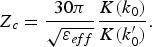
. Therefore, the characteristic impedance of the CPW can be determined by
$Q_1 = \displaystyle{1 \over 2}\displaystyle{{K(k_0 )} \over {K(k_0^{\prime} )}}\left( {\displaystyle{{K(k_3^{\prime} )} \over {K(k_3 )}} + \displaystyle{{K(k_1^{\prime} )} \over {K(k_1 )}}} \right),\;Q_2 = \displaystyle{1 \over 2}\displaystyle{{K(k_0 )} \over {K(k_0^{\prime} )}}\displaystyle{{K(k_2^{\prime} )} \over {K(k_2 )}}$
. Therefore, the characteristic impedance of the CPW can be determined by
 $$Z_c = \displaystyle{{30\pi} \over {\sqrt {{\rm \varepsilon} _{eff}}}} \displaystyle{{K(k_0 )} \over {K(k_0^{\prime} )}}.$$
Based on the above analysis, the impact of the separation distance, and the width of the signal and ground traces on the FGCPW line characteristic impedance, Z c , is investigated. As illustrated in Fig. 2(a), at 40 GHz for a fixed gap size of s = 15 μm, increasing the signal strips width w s decreases the impedance, while increasing the ground strip width w g has relatively small impact on the impedance Z c . Furthermore, Fig. 2(b) shows that an increase in the signal separation s increases the characteristic impedance.
Characteristic impedance of the FGCPW at 40 GHz as a function of signal strip width (w
s
) for (a) $s = 15{\kern 1pt} \;{\rm \mu m}$
and different ground strip widths, and (b)
$s = 15{\kern 1pt} \;{\rm \mu m}$
and different ground strip widths, and (b) $w_g = 30\;{\kern 1pt} {\rm \mu m}$
and different gap sizes.
$w_g = 30\;{\kern 1pt} {\rm \mu m}$
and different gap sizes.
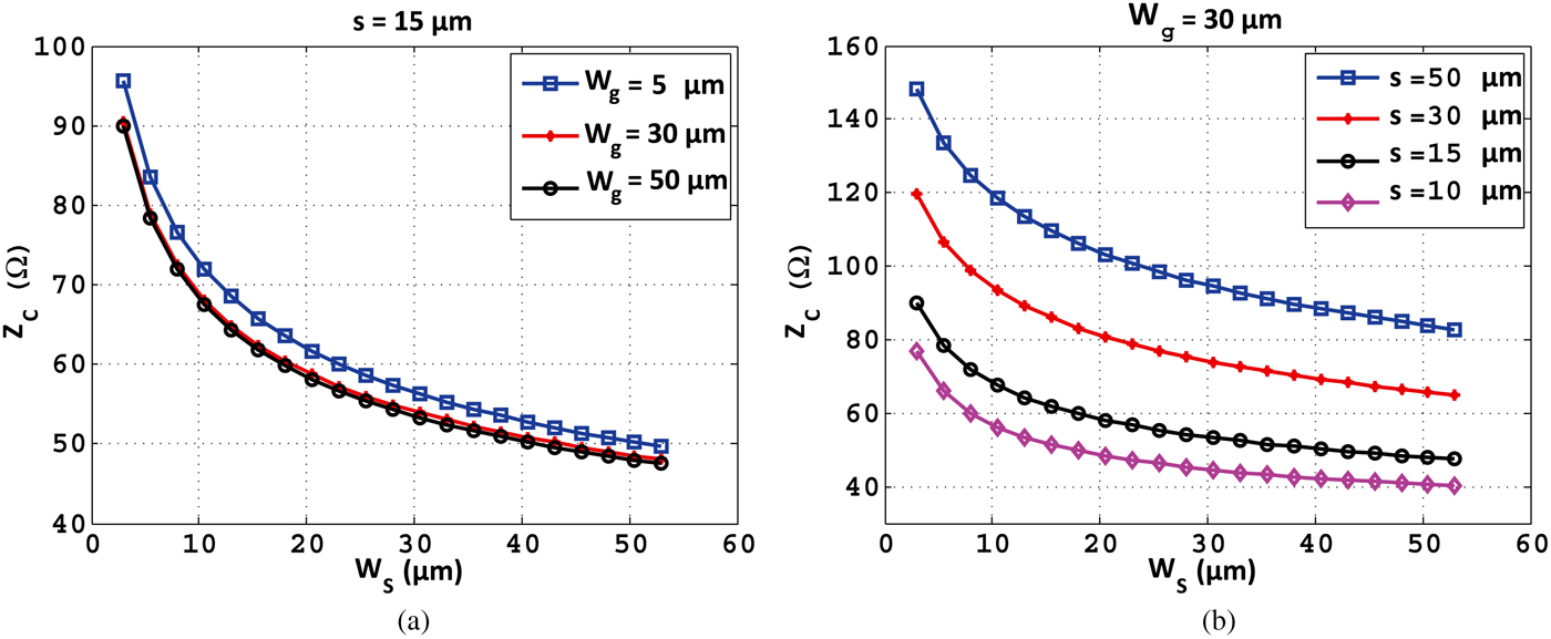
To characterize the proposed waveguide structure with its data transmission, high-speed test and measurement equipments are exploited and a transmission line impedance of 50 Ω is set as a design requirement. In such context, as shown in Fig. 2(b), the optimal signal strip dimension for a 50 Ω FGCPW line is w
s
= 50 μm. Additionally, according to Fig. 2(a), the requirement of 50 Ω for a signal strip width of $50{\kern 1pt} \;{\rm \mu m}$
is met if the values for the two other parameters w
g
and s are 30 μm and 15 μm, respectively. The proposed structure is fabricated through a custom fabrication process. The complete fabrication process is detailed in [Reference Banan, Tait, Liboiron-Ladouceur and Berini19].
$50{\kern 1pt} \;{\rm \mu m}$
is met if the values for the two other parameters w
g
and s are 30 μm and 15 μm, respectively. The proposed structure is fabricated through a custom fabrication process. The complete fabrication process is detailed in [Reference Banan, Tait, Liboiron-Ladouceur and Berini19].
III. CHARACTERIZATION OF THE FGCPW
After the design and fabrication, the transmission response of the waveguide structure is characterized. Figure 3 illustrates the schematic of the electrical S-parameter measurement set-up using a 50 MHz–40 GHz vector network analyzer (VNA). An electrical input power of −10 dBm is provided by the VNA which is used to excite and capture the quasi-TEM mode of the proposed FGCPW. The waveguide is excited using an electrical GSG probe at its input. The transmitted signal is collected with another GSG probe at the output of the waveguide structure. Both probes are controlled with three-axis micropositioners. Prior to the measurements, the set-up is calibrated using a calibration substrate for short, open, load (50 Ω) as well as through, i.e., standard short, open, load, and through (SOLT) calibration, to normalize the impact of the 40 GHz RF probes and cables on the measurements.
Schematic of the experimental set-up for the S-parameter measurements.

Figure 4 presents the S-parameter magnitude results for various 3 mm long waveguides with a 50 µm wide signal strip (w s ), three different ground strip widths (i.e., w g of 5, 20, and 30 µm) and seven different separation distances (i.e., s of 2, 5, 8, 10, 12, 15, and 18 µm). As shown in Fig. 4, all structures show a transmission (S 21) drop and high reflections (S 11) at low frequencies up to approximately 1 GHz. Afterwards, the transmission improves up to approximately 12 GHz, and then decreases as frequency increases. The transmission drop at low frequencies is largely due to reflection caused by impedance mismatch in the structure. This will be discussed in Section IV. The measurement shows that the wider the ground strips w g and separation distance s the lower the transmission loss. The results confirmed that a wider ground strip leads to lower reflection due to improved impedance match (i.e., see Fig. 2), whereas, a larger separation distance leads to higher reflections.
Measured transmission (S 21) and reflection (S 11) of the 3 mm long waveguides with w s = 50 μm for various separation distances s for w g = 30 μm (in (a), and (d)), w g = 20 μm (in (b), and (e)), and w g = 5 μm (in (c), and (f)), over the frequency range of 50 MHz to 40 GHz.

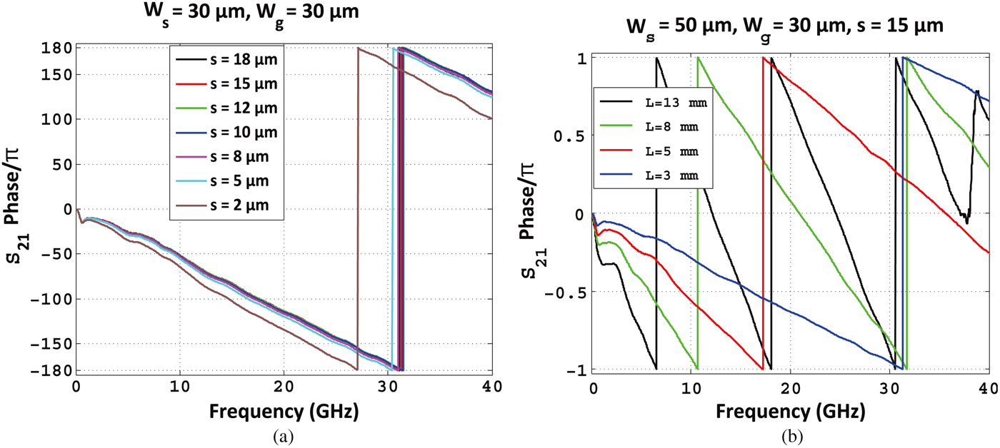
Additionally, Fig. 5 shows the measured transmission (S 21) phase profile of the 3 mm long waveguides with (w s ) = 50 μm (w g ) = 30 μm and various separation distances s (in Fig. 5(a)), and for different lengths while s = 15 μm (in Fig. 5(b)). As illustrated, the phase response of the line is linear suggesting that the line is not dispersive.
Measured transmission (S 21) phase profile of the waveguides with w s = 50 μm, w g = 30 μm; (a) for the length of 3 mm and various separation distances s, and (b) for various lengths and a fixed separation distance s = 15 μm, over the frequency range of 50 MHz to 40 GHz.
IV. CIRCUIT MODEL AND TRANSMISSION PARAMETERS EXTRACTION
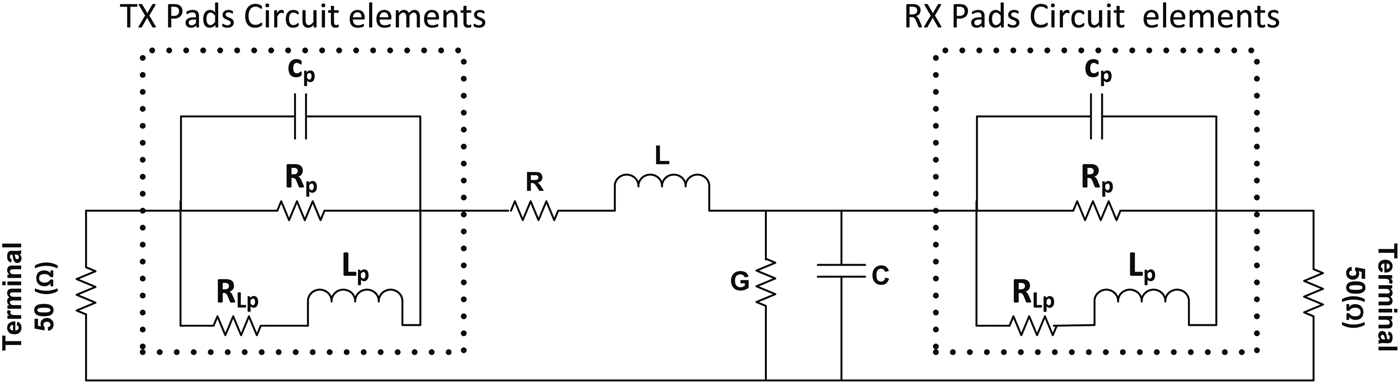
Transmission line models are necessary to predict interconnect properties such as impedance and propagation constant. In this work, the transmission line is modeled on the basis of its lumped circuit elements which requires careful consideration due to its operation frequency range from direct current (DC) to a few tens of GHz. Additionally such a circuit model should also reflect the effect of the parasitic elements originating from the pads and their connections to model the structure as precise as possible. The lumped circuit parameters of this accurate equivalent circuit model for the fabricated FGCPW are obtained using Advanced Design System (ADS) commercial software. In order to improve the accuracy of the model, the parasitic impact of the two electrical pads at both ends and their connections is modeled and compared with its conventional circuit model without these imposed effects, i.e., see Fig. 1(b). Indeed, the pads and their connections pose additional RLC parasitic elements to the FGCPW transmission line which degrade the performance of the device in terms of transmission (S 21), particularly at low frequencies (i.e., below 10 GHz). This issue can be mainly associated with the sheet resistance, inductance, and capacitance of the pads and their connections.
Figure 6 demonstrates the accurate equivalent circuit model with the parasitic elements of the pads. To extract the values of the elements in the circuit model shown in Fig. 6, the measured S 21 data are imported into ADS and the difference between the transmissions of the circuit model and the measured S 21 is minimized. This process is done by applying the “Random” and “Gradient” optimization methods in the OPTIM engine of ADS. Table 1 summarizes the results for different waveguide lengths with a signal width (w s ) of 50 µm, ground strips (w g ) of 30 µm width, and a 15 µm gap (s).
Equivalent lumped circuit model of the FGCPW transmission line in which the effects of the pads and their connections are considered.
Extracted lumped circuit element values from the measured S-parameters based on the distributed circuit model presented in Fig. 6 for different lengths of the transmission line with w s = 50 μm, w g = 30 μm, and s = 15 μm.

As expected, increasing the length results in an increase in the transmission line's resistance R and inductance L. It also reveals that the line's conductance G (or dielectric loss) is negligible. Additionally, the line capacitance C of the proposed FGCPW is approximately two orders of magnitude less than conventional CPW structures on silicon substrate. It should be underlined that the small divergence in the parasitic parameters of the TX and RX pads and their connections for different lengths is mainly associated with the optimization process of the ADS software to find the minimum difference between the transmission of the circuit model and the measured S 21.
Figure 7 shows the measured transmission S 21 (solid line) for the four devices length investigated in Table 1. Overlaid are the calculated transmission responses obtained from the extracted circuit element values based on both the conventional circuit model from the Telegrapher's equations [Reference Eisenstadt and Eo20] (black dash line) where the pads are not considered, and the customized accurate model (red dash-dotted line) which includes the pads parasitic circuit elements. The circuit model results for four different lengths are plotted in two figures for proper scaling of the magnitude.
Measured S 21 parameter (solid line) along with the modeled transmission responses without and with considering the parasitic elements of the pads and connections, for the conventional circuit model (dashed line) and the accurate circuit models (dash-dot), respectively. The waveguides are 3, 5, 8, and 13 mm long with 50 µm signal strip width, 30 µm ground strip width, and 15 µm separation distance over the frequency range of 50 MHz to 40 GHz.
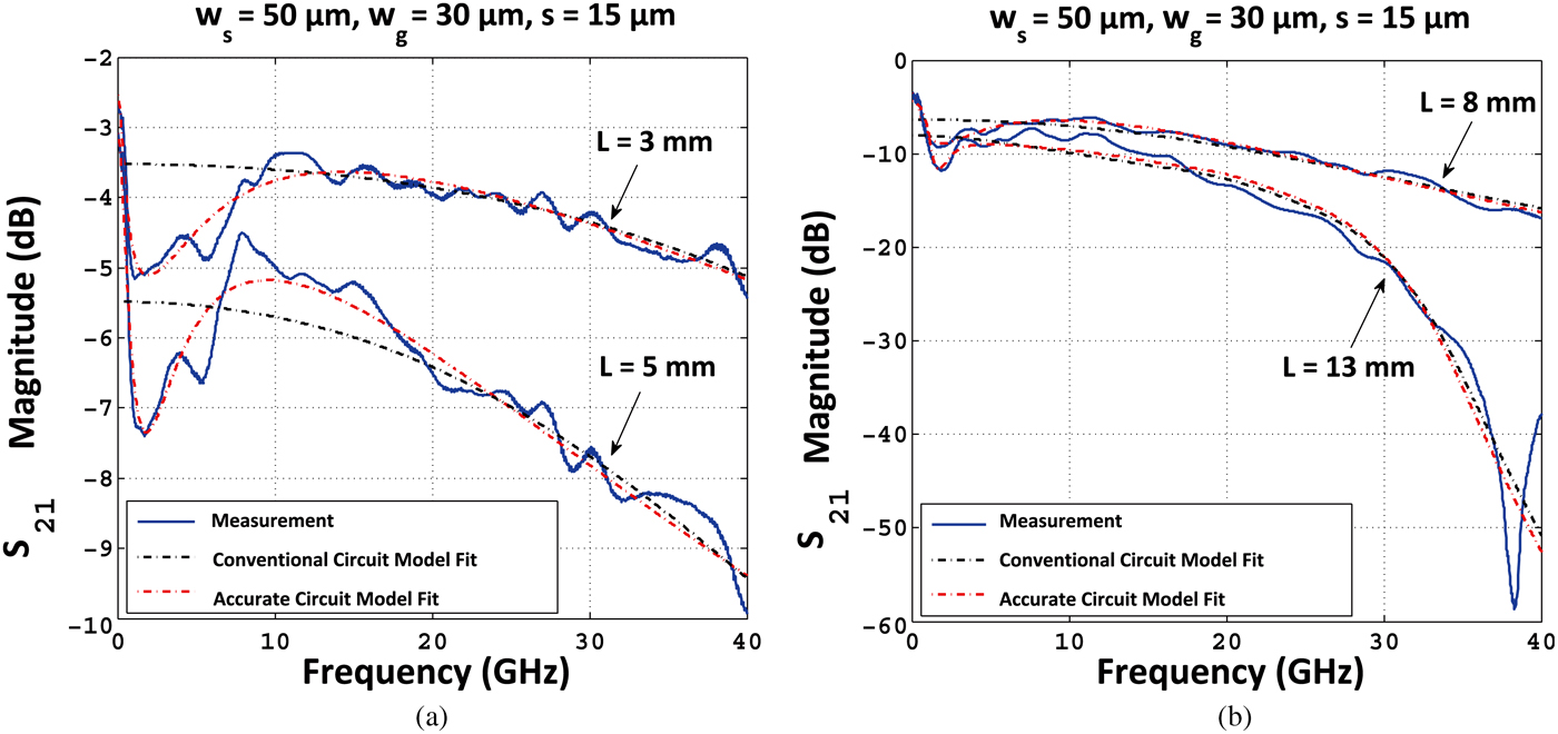
As can be inferred from the figure, the conventional and custom circuit models for different lengths provide approximately the same results for frequencies above 10 GHz, while they differ at lower frequencies due to the effect of the parasitic elements originating from the pads and their connections, in which they act as parallel lossy LC oscillator (i.e., parallel RLC circuit). This can be confirmed by calculating the equivalent impedance (Z in ) of the lumped circuit model as a function of frequency, in which the parallel RLC components cause high impedance mismatch at the input at low frequencies (below 10 GHz) resulting in high reflections. Therefore, the impact of the pads at lower frequency is significant and must be taken into account in order to have an optimized structure over the entire frequency range.
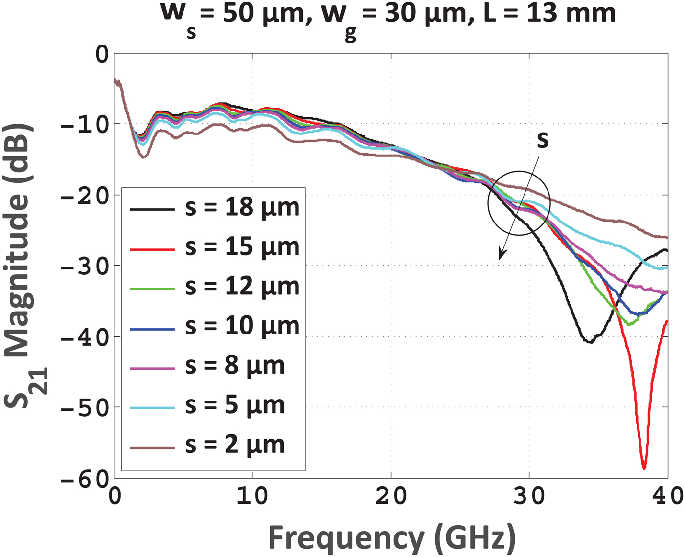
Figure 8 shows that the 13 mm long transmission line exhibits a resonance at 38 GHz which suggests the formation of a standing wave within the waveguide structure. Indeed, an impedance mismatch between the transmission line and the load will lead to reflections. If the incident signal is a continuous AC (alternating current) waveform, these reflections will mix with more of the oncoming incident waveform to produce stationary waveforms (i.e., standing waves) [Reference Connor21]. Measurement results depicted in this figure show that the resonance becomes weaker with smaller separation distances.
Measured transmission of 13 mm long lines with w s of 50 µm and w g of 30 µm for different separation distances.
V. ENVISIONED APPLICATIONS
The hybrid structure presented in this work allows for data transmission in both the optical and electrical domains. One envisioned application is short interconnects in advanced packaging such as interposers [Reference Lee, Lee, Kim, Park and Sim22]. To implement such a hybrid transmission line, the cross-sectional dimensions of the structure can be designed (referring to Section II) to satisfy the impedance matching condition with any target electronic interface. Also, the electrical interconnects are implemented using fine pitch micro bumps (20 µm, [Reference Banijamali, Ramalingam, Liu and Kim23]). Thus, depending on the available fabrication technology, the ground pads as well as the signal connection (or pad) can be designed as small as possible to minimize their parasitic effects (referring to Section IV), and that they are compatible with micro bumps for the electrical interface. Additionally for efficiency, the laser source must be ideally edge coupled to the ground strips of the waveguide. As such, edge emitting semiconductor lasers are a good fit.
Bandwidth and reach of the discussed transmission line is comparable to recent works [Reference Mensink, Schinkel, Klumperink, van Tuijl and Nauta24, Reference Nazari and Emami-Neyestanak25]. The bandwidth density of the proposed waveguide structures is 1 Gb/s/μm [see reference Reference Banan, Hai, Berini and Liboiron-Ladouceur11] compared with 1.16 Gb/s/μm in [Reference Mensink, Schinkel, Klumperink, van Tuijl and Nauta24] and 1.5 Gb/s/μm in [Reference Nazari and Emami-Neyestanak25]. In the former case, signal and ground trace widths are 0.54 µm separated by 0.64 µm, supporting 2 Gb/s data rate over a 10 mm length. The bandwidth density of the proposed hybrid structure in this work is limited mainly by the fact that the line's impedance was designed to be 50 Ω for characterization purpose. By relaxing this limitation to a slightly larger impedance (see Fig. 2(a)), the lateral dimension can be reduced with a narrower signal width w s for a larger bandwidth density.
The proposed structure has inherently unlimited bandwidth density due to the fact that it supports optical signal. Optical bandwidth limitations originate from electrical-to-optical (EO) and optical-to-electrical (OE) converters. An energy-efficient configuration for this structure is to provide on-chip and chip-to-chip interconnects by allocating high data rate channels to the optical section and sending lower data rates (e.g., control signals) over the electrical section. To reach this goal, assuming CMOS electrical transmitter and receiver designs with high impedance front-ends, the signal trace width can be as small as 0.5 µm and the ground traces width can be designed to be as small as 5 µm. The separation distance between the signal and ground traces should be such that the optical modes on the ground strips do not overlap with the signal strip. For the aforementioned ground width, a 10 µm separation must be considered for 20 nm thick ground strips. Structures with thicker strips (35 nm) can have 7 µm separation distances. Essentially, the geometry of the proposed structure can be optimized efficiently for a given characteristics of electrical transmitter and receiver.
VI. CONCLUSION
The microwave performance of a novel FGCPW waveguide was presented. The hybrid waveguide is capable of supporting microwave and optical signals, simultaneously. An existing conformal mapping method was defined to optimize the geometrical parameters of the transmission line to match a given characteristic impedance. Frequency dependent parameters were then extracted from experimental measurements of fabricated waveguides with different dimensions using a conventional circuit model. A more accurate circuit model enabled to take into account the impact of the parasitic elements from the ground pads at lower frequencies. Thus, it was realized that to improve the performance of the structure, the pad effects should be minimized by reducing pad area (i.e., less capacitance) and length of the connection (i.e., less resistance). The methodology presented allows for this novel structure to be used for interconnects of a few millimeters enabling a bandwidth density of 1 Gb/s/μm and higher.
ACKNOWLEDGEMENTS
The authors thank CMC Microsystems for providing the high-speed electrical measurement equipment. This work was funded by the Natural Sciences and Engineering Research Council of Canada (NSERC) Discovery program.
 Behnam Banan received his B.Sc. in Material Science in 2008 from University of Tehran, Iran and his M.Sc. in Nanotechnology with the major in Physics in 2010 from Royal Institute of Technology (KTH), Stockholm, Sweden. He is currently Ph.D. candidate in the Electrical and Computer Engineering Department at McGill University. The focus of his research is optical and electrical interconnects for on-chip and chip–chip communication.
 Farhad Shokraneh received his B.Sc. in Electrical Engineering from Shahed University of Tehran, Iran in 2009 and his M.Sc. degree in Electrical Engineering-Communication Systems from Lund University, Sweden. He is currently a Ph.D. candidate at the Department of Electrical and Computer Engineering, McGill University with the main focus on photonics integrated circuits, optical–electrical interconnects, and microwave-photonics.
 Pierre Berini (F'11) received his Ph.D. and M.Sc.A. degrees in Electrical Engineering from École Polytechnique de Montréal, Canada, and his B.E.Sc. and B.Sc. degrees in Electrical Engineering and Computer Science, respectively, from the University of Western Ontario, Canada. Dr. Berini is Professor of Electrical Engineering, Professor of Physics, University Research Chair in Surface Plasmon Photonics, and Director of the Centre for Research in Photonics at the University of Ottawa (CRPuO). He was the Founder and Chief Technology Officer of a venture capital-financed company and he collaborates on an ongoing basis with industry. Dr. Berini has received an NSERC Steacie Fellowship, an NSERC Discovery Accelerator, a Premier of Ontario Research Excellence Award (PREA), the University of Ottawa Young Researcher of the Year Award, an URSI Young Scientist Award, a George S. Glinski Award for Excellence in Research, and is a Canada Foundation for Innovation researcher. Dr. Berini is a Fellow of the IEEE and of the Canadian Academy of Engineering, and he is a member of the OSA and SPIE. He has published seven book chapters, approximately 300 scientific and technical papers in peer-reviewed periodicals and conference proceedings, and is an inventor or co-inventor on 20 patents. He was an Associate Editor of Optics Express and is currently an Associate Editor of Nanophotonics. He contributes on an ongoing basis to the organization of several international conferences in photonics. His research interests span many areas of optics and photonics, with surface plasmons and their applications being of particular interest.
 Odile Liboiron-Ladouceur (M'95, SM'14) received the B.Eng. degree in Electrical Engineering from McGill University, Montreal, QC, Canada, in 1999, and the M.S. and Ph.D. degrees in Electrical Engineering from Columbia University, New York, NY, USA, in 2003 and 2007, respectively. Prior to her graduate studies, she worked in the industry as an applications engineer at Teradyne in Boston, MA (1999–2000) and as a test engineer at Texas Instruments in Dallas, TX (2000–2002). She is currently an Associate Professor at the Department of Electrical and Computer Engineering, McGill University. Dr. Liboiron-Ladouceur holds the Canada Research Chair in Photonics Interconnect. She is a Senior member of the IEEE and a member of the OSA and SPIE. She as been elected on the Board of Governors of the IEEE Photonics Society (2016–2018). She is an Associate Editor of the IEEE Photonics Society since 2009, and the IEEE Photonics Society Montreal Chapter Chair. She has been on several technical program committees at international conferences. Her research interests include optical systems, photonic integrated circuits, and photonic interconnects. She is the author or coauthor of 43 journal papers and 93 papers in conference proceedings.


 Open access

