

Introduction
Wide-band frequency multiplier chains with sufficient output power above 200 GHz are of immense importance used as transmitters or to drive the mixer's local oscillator (LO) port in transceivers chip-sets. The main challenges for such circuits are to achieve flat frequency response with as high DC-to-RF efficiency as possible and filtering out the unwanted harmonics. Different solutions have been proposed to realize such circuits. Fundamental frequency oscillators at 240 GHz [Reference Voinigescu, Tomkins, Dacquay, Chevalier, Hasch, Chantre and Sautreuil1] or at 120 GHz followed by a frequency doubler [Reference Shopov, Balteanu, Hasch, Chevalier, Cathelin and Voinigescu2], although being power-efficient solutions, they are accompanied by constrains and tradeoffs concerning the phase noise due to the degraded quality factor of varactors at such frequencies. Also, in coherent systems when LO synchronization is required, the design of a phase locked loops divider (PLL) becomes a challenge. A second solution is the multiplication of a low frequency signal performed by LO chain consisting of cascaded frequency multipliers [Reference Momeni and Afshari3,Reference Sarmah, Heinemann and Pfeiffer4]. The latter option suits well for applications requiring wide tuning range and LO synchronization. It also allows for the usage of available PLLs at lower frequencies with optimized phase noise performance. The later solution might be more power consuming due to the multi-stage nature of such circuits. An efficient power budget distribution becomes of high importance to achieve acceptable power efficiency. Maximum power efficiency is achieved when the different stages are at the onset of saturation. Another point to consider when designing high multiplication factor LO chain is the LO spurs, which is critical for wideband communication systems as the spurious LO signal might lead to parasitic noise folding and unwanted image signals down-converted on top of the desired signal. That explains why the inter-stage matching circuits within the LO chain need to be carefully designed and centered within the band in order to reject spurious unwanted harmonics and frequency intermodulation products.
To enhance the achievable output power, power combining of multipliers array has been proposed in the literature where power combining might be either on-chip or wireless [Reference Lin and Rebeiz5,Reference Schmalz, Borngr”aber, Debski, Elkhouly, Wang, Neumaier and Hubers6] In this work LO multiplier-by-8 chain is presented, aiming to deliver 0 dBm of power, which is typically sufficient to saturate active double-balanced Gilbert cell mixers, across wide bandwidth with a fully differential architecture. This paper is organized as follows: in the section “Circuit design”, the LO chain architecture and the design details are discussed. The section “Measurement results” provides the measurement results and the section “Conclusion” concludes the paper.
Circuit design
LO multiplication chain architecture
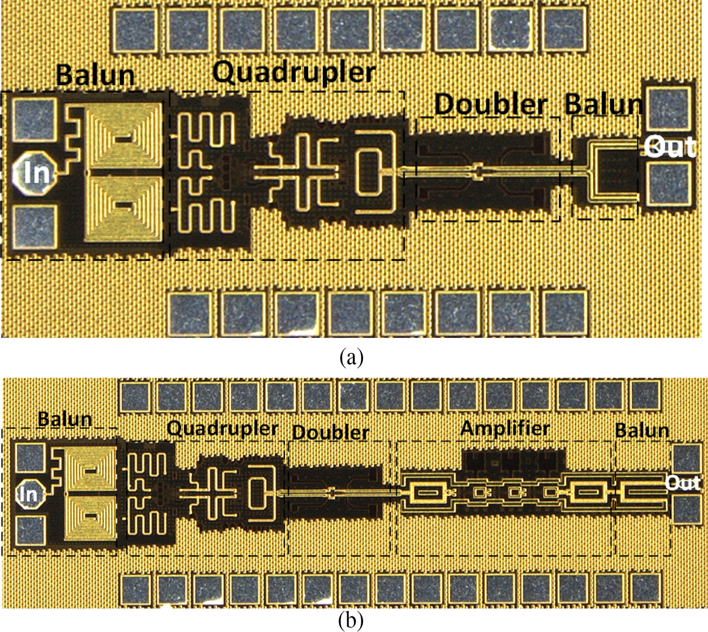
As shown in Fig. 1, a single ended 30 GHz signal (LO in) is fed through a spiral Marchand balun to a single stage Gilbert cell-based frequency quadrupler. The output is amplified by a single stage cascode amplifier which drives a 240 GHz frequency doubler, the die photo of this test structure is shown in Fig. 2(a). In a second version of the LO chain an output wideband amplifier is deployed in order to achieve 0 dBm output power, where the die photo of the full LO chain is shown in Fig. 2(b). Marchand baluns at 240 GHz were utilized in both versions to allow for on wafer measurements. The design is implemented in a standard 0.13 nm SiGe:C BiCMOS technology from IHP. The technology offers hetero-junction bipolar transistors (HBT) with a cutoff frequency and maximum frequency of oscillation of 300 GHz and 500 GHz, respectively. It has two thick metal layers: TopMetal2 (TM 2) and TopMetal1 (TM 1) with 3 and 2 µm thickness, respectively, and five thin metal layers made of Aluminum.
Schematic of the integrated LO chain.

Die photo of LO chain with no output amplifier (Version 1) (a) and with output amplifier (Version 2) (b).
Wideband 30 GHz Marchand balun
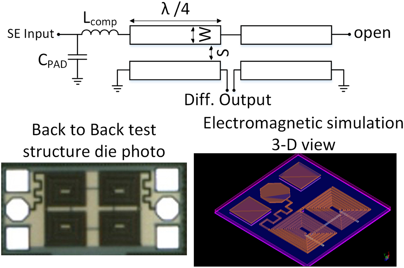
To enable the use of differential architecture, a spiral planar edge-coupled Marchand balun, shown in Fig. 3, was implemented at the input. The balun is designed using the top metal layer (3 µm thick) with a ground plane at a distance of 8.1 µm. The conductor width (W) and spacing (S) of 4 µm each were chosen to achieve both wide band operation without sacrificing the ripple in the insertion loss at the middle of the band, and a good input return loss (S 11) across the whole band, as explained in [Reference Lin, Wu, Yeh, Fu, Chang, Lin and Wang7,Reference Qian and Luo8]. Another important aspect when designing the conductor width is the self-resonance of the whole structure, caused by the parasitic capacitance in between the turns. An inductive compensation structure at the input (L comp) compensates for the pad capacitance (C PAD). Simulation results show an amplitude and phase imbalance of ±0.5 dB and ±2.5° within the band 10–50 GHz as shown in Fig. 4. Also the insertion loss for the differential mode (Diff.) and common mode (CM) to single ended input (SE) shows a rejection of approximately 25 dB across the whole band.
Wideband Spiral Marchand balun schematic and full electromagnetic (EM) view.
Simulated S-parameters and gain/phase imbalances for the wideband Marchand balun.

A back-to-back test structure, shown in Fig. 3, was manufactured and measured, the measurement results in Fig. 5 show a 3-dB bandwidth of 38.5 GHz from 14 to 52.5 GHz, with a fractional BW of 116 % and a minimum insertion loss of 2.35 dB. The S 11 is below −8 dB across the 3-dB bandwidth. The balun occupies an area of 260 µm × 150 µm.
Measurement and simulation results for the back to back test structure of the 30 GHz Marchand balun.

120 GHz frequency quadrupler design
Different architectures have been proposed in the literature to implement frequency quadruplers, frequency doublers have been either cascaded [Reference Sarmah, Heinemann and Pfeiffer4] or stacked in order to reduce the power consumption by reusing the bias current [Reference Jamal, Eissa, Borngräber, Ng, Kissinger and Wessel9]. The latter solution, although has a low power consumption and larger bandwidth because of the less number of stages, it suffers from low output power due to the limited output power from the input push-push doublers which subsequently does not saturate the second switching quad. In order to achieve low-power consumption and sufficient output power, a novel architecture is implemented in this work where a compact frequency quadrupler based on a single Gilbert cell converts a 30 GHz input frequency directly into 120 GHz. It consists of a quadrupler core and an output buffer. The Gilbert cell core shown in Fig. 6(a), which is conventionally utilized as a doubler, generates strong fourth harmonic by emphasizing the nonlinearities (3rd harmonic) of the transconductance stage (Q n – Q p) which then mixes with the fundamental tone within the switching quad. Although achieving lower DC power consumption compared with the cascaded linear multiplying doublers topology, the utilization of the input transconductance stage nonlinearities degrades the spurious performance of such an architecture. The output amplifier, shown in Fig. 6(b), behaves as a tuned filter at the fourth harmonic to reduce the unwanted 3rd and 5th harmonics. This can be observed in Fig. 7 where the simulated output power for the 3rd, 4th, and 5th harmonics are plotted across the input frequency. The output amplifier increased the rejection to the 3rd harmonic by 15 dB and to the 5th harmonic by 5 dB at 30 GHz input frequency. The circuit achieves an output power of 2.7 dBm at 120 GHz with a 3 dB bandwidth of 25 GHz, and a drain efficiency of 4.1%.
Schematic of the 120 GHz frequency quadrupler (a) and 120 GHz amplifier (b).

Simulated 3rd, 4th and 5th LO harmonics at quadrupler core output and amplifier output (P in = 4 dBm).

240 GHz frequency doubler design
Although the push-push frequency doubler architecture allows for higher power efficiency [Reference Shopov, Balteanu, Hasch, Chevalier, Cathelin and Voinigescu2], it requires a balun at the output in order to drive double-balanced Gilbert cell mixers. The balun phase and gain imbalance are translated into common mode excitation for the mixer which degrades the LO to RF isolation, this is crucial especially for direct conversion transmitters. On top of that, single-ended signaling causes poor supply and ground noise rejection, and possible feed-back loops. For these reasons a fully differential Gilbert cell-based doubler, shown in Fig. 8(a), is utilized in this work to keep the differential architecture of the LO chain [Reference Sarmah, Heinemann and Pfeiffer4,Reference Bredendiek, Pohl, Aufinger and Bilgic10]. As the frequency doubler is normally in the large signal mode of operation, hence the input transistors (Q n – Q p) and the switching quad transistors (Q 1 – Q 4) are sized for maximum f T based on the under drive current consumption.
Schematic of the 240 GHz frequency doubler (a) and its full EM simulation view (b).
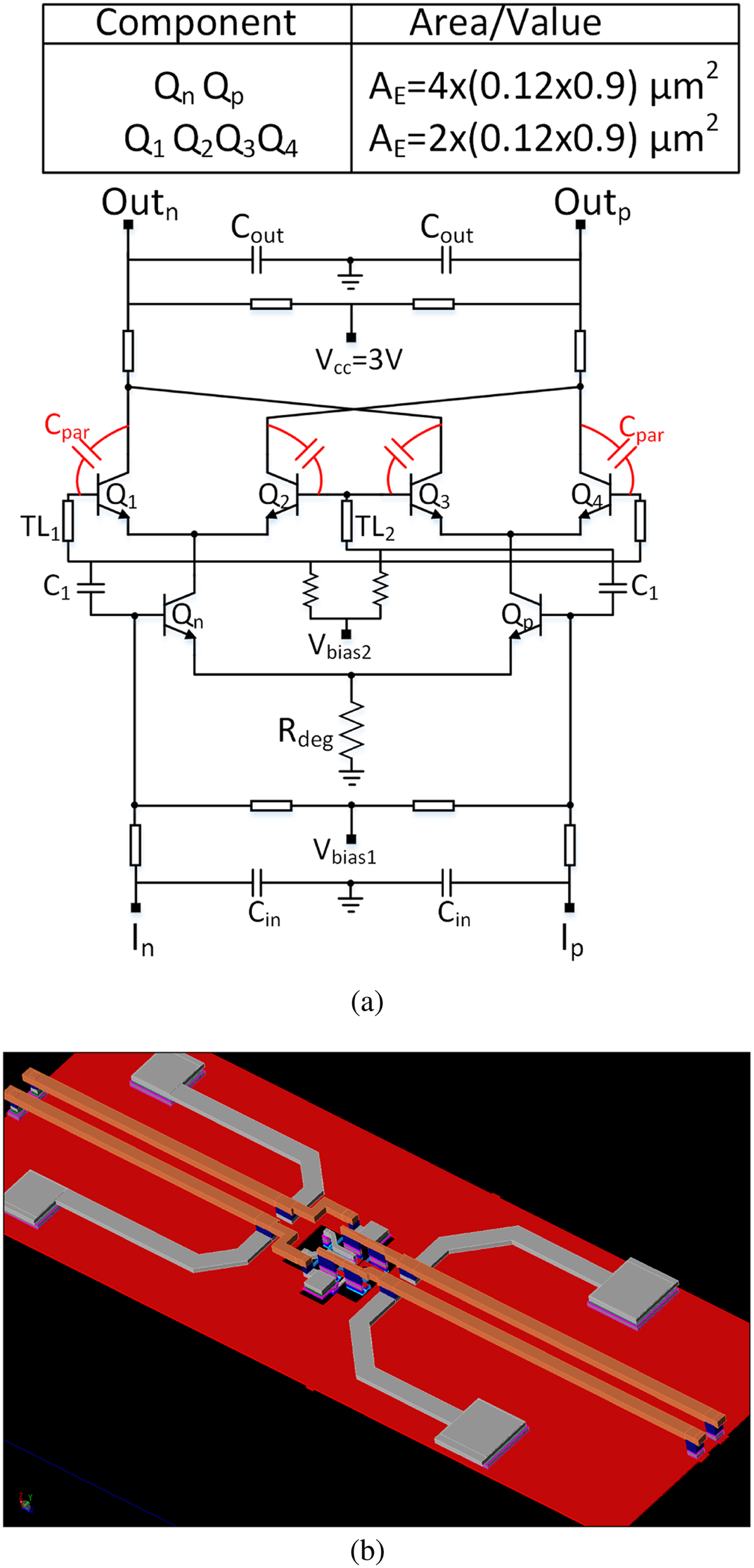
The core of the frequency doubler is optimized to reduce the parasitic capacitance between the input of the switching quad transistors (Q 1 – Q 4) and the doubler's differential output, highlighted as C par in Fig. 8(a). This is critical at such high frequencies because large C par might lead to a leaking input signal to the output and so significantly deteriorates the doubler conversion gain. Full electromagnetic (EM) simulation is used as shown in Fig. 8(b) to capture the spurious leakage accurately. For the sake of better output signal differentiality a degeneration resistor Rdeg of 10 Ω is utilized to degenerate the common mode signal. With optimized signal routing within the doubler core, phase and gain imbalance of <5° and 1 dB respectively, were simulated across the whole band of interest as shown in Fig. 9. In order to minimize the conversion loss of the doubler, the transmission lines (TL 1 − TL 2) are optimized to keep a 90° phase shift between the input base voltage and emitter current to the switching quad, taking into account the effect of the parasitic inductance within the doubler core.
Simulated gain and phase imbalance between doubler differential outputs w and w/o degeneration resistance.

A 3 dB bandwidth of 60 GHz with a maximum output power of −6 dBm (P in = 0 dBm) was simulated for the doubler with good in/out matching as shown in Fig. 10(a). While the power sweep in Fig. 10(b) for Fout = 240 GHz shows that conversion gain of −6.2 dB is achieved at an input power of −3 dBm, while the output power achieves approximately 0 dBm at an input power of 8 dBm, dissipating a power consumption of 27 mW. This leads to maximum drain efficiency of 3.7%.
Simulation result of the doubler I/O return losses and output power across frequency for P in = 0 dBm (a) and the doubler saturated output power and conversion gain across input power for Fout = 240 GHz (b).

240 GHz amplifier design
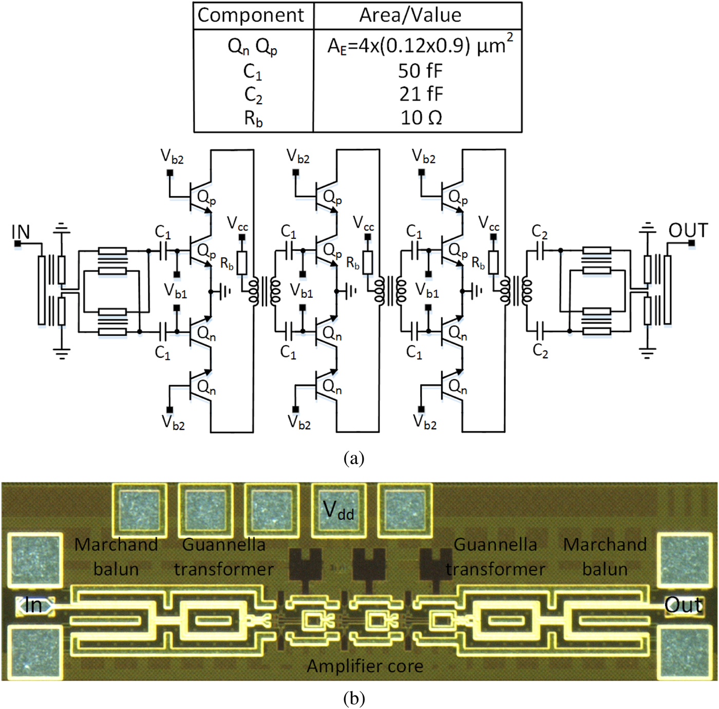
In order to deliver a power level of 0 dBm, a fully differential 240 GHz amplifier offering about 10 dB gain was placed at the output of the LO chain, as in the second version of the LO chain shown in Fig. 1. The used 240 GHz amplifier is a fully differential 3-stage cascode with Guanella impedance transformers [Reference Guanella11], used for input and output matching and transformer-based inter-stage matching. An amplifier schematic view is reported in Fig. 11(a). A mid-size transistor has been chosen for trade-off between power consumption, output power and gain. The collectors have been biased through the transformers' center tap, using an additional 10 Ω bias resistor R b for avoiding inter-stage feedbacks through the supply lines. The transformers have been designed making extensive use of EM simulations. Input and output matching have been performed with the help of Guanella impedance transformers, which transforms in a wideband fashion the reference impedance of 100–25 Ω, closer to the amplifier's input and output impedances. In other words, through a Guanella transformer the 100 Ω reference impedance at which the amplifier has to be matched can be lowered within the whole band of interest by a factor 4–25 Ω, an impedance which is close to the one shown by base, for input matching, and collector, for output matching, of the core transistors. In order to verify its performance, the amplifier has been manufactured and measured as a stand-alone circuit, and its die photo is shown in Fig. 11(b). For measurement purposes, the differential input and output must be converted by integrated Marchand baluns to single ended signals. A WR-3.4 (220–325 GHz) vector network analyzer frequency extension modules have been used to characterize the amplifier. In Fig. 12 on-wafer measurement and simulations of the stand-alone amplifier are compared in terms of S-parameters. The high degree of agreement validates the design procedure. Within a bandwidth as wide as 50 GHz, a gain of 9 dB has been measured, at a power consumption of 100 mW.
Schematic (a) and die photo (b) of the 240 GHz amplifier.
Measured and simulated S-parameters of the 240 GHz amplifier.

LO chain power budget
To explore the power budget across the LO chain, Fig. 13 shows the simulated power level at the output of each stage across the input power. It is clear that the highest efficiency will be achieved if each and every block is operating at the onset of saturation, but few dBs as a margin is crucial when planning systems at such frequencies. It can be observed that the LO chain saturates at input power of approximately −4dBm, where the quadrupler drives the doubler with −2 dBm. The doubler drives the amplifier with a power of −8dBm, which guarantee that the whole chain is operating at the onset of saturation with some margin, leading to a saturated output power of approximately 0 dBm.
Simulation results for the output power after each stage, (Quadrupler output at 120 GHz, doubler output at 240 GHz and amplifier output at 240 GHz), across input power at input LO=30 GHz.

Measurement results
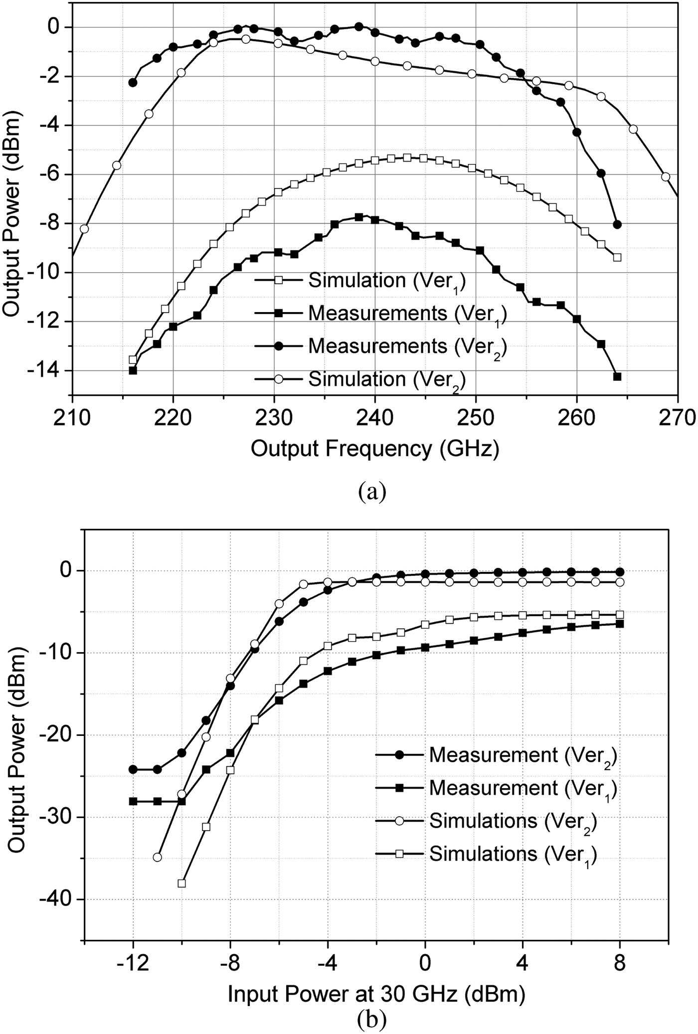
At first the LO chain without the output amplifier (Version 1), whose die photo is shown in Fig. 2(a), was measured on wafer. An external low-frequency source was applied at the input of the multiplier-by-8 chain varying its frequency and power level, while the output power was measured using an absolute power meter (Erickson calorimeter PM4). A saturated output power of −8 dBm was measured with a 3 dB BW of 32 GHz as shown in Fig. 14(a). A wider bandwidth of 40 GHz was measured for the full LO chain with the amplifier (Version 2), shown in Fig. 2(b), with a saturated output power of 0 dBm as shown in Fig. 14(b). These power levels were compensated for the probe loss of 3 dB but not for the on chip balun and pad which contribute with a loss of approximately 1 dB each.
Measured and simulated, saturated output power of the 8th harmonic across RF frequency for Ver1 and Ver2 at P in = 4 dBm (a) and output power across input power for Ver1 and Ver2 for f out = 240 GHz (b).
Output LO harmonics of the frequency multiplier chain were measured on wafer within the G-Band frequency range, 140–220 GHz, in order to monitor the 5th, 6th, and 7th harmonics. The measurement results in Fig. 15 shows that the highest harmonic is the 7th harmonic with a 25 dB of rejection comparedwith the fundamental signal (8th harmonic) which was plotted in Fig. 14(a). Comparing the harmonics rejection of the first version with the one in the second version, it is clear that the external amplifier enhanced the rejection to the 5th and 6th harmonics as the frequencies are out of the amplifier effective bandwidth, while no enhancement can be observed in the 7th harmonic as its frequency range lies within the amplifier bandwidth. A better rejection of the 7th harmonic can be achieved by further filtering of the 3rd harmonic at the quadrupler output by adding extra tuned amplification stage. Good match between measurements and simulations is achieved through full EM simulation of different circuit parts. A temperature of 45°C was used in simulation to account for the real chip operation temperature. Table 1 compares this work with state-of-the-art single element LO chains and frequency sources above 200 GHz. With a 3 dB bandwidth of 40 GHz and saturated output power of 0 dBm the presented LO chain provides the highest bandwidth with such output power and inherently differential outputs when compared to the state-of-the-art. It suits well as LO chain to feed balanced Gilbert cell mixer in transceiver's front ends. By utilizing a VCO with 5 GHz of tuning range at 30 GHz and average phase noise (PN) of −100 dBc/Hz at 10 MHz offset frequency [Reference Kucharski, Herzel, Ng and Kissinger14], locked frequency sources of 40 GHz bandwidth in the 240 GHz frequency band and estimated phase noise of −102 dBc/Hz at 10 MHz offset (PN240GHz = PN300GHz + 20log(8)), can be realized.
Measured LO harmonics at the output across the input LO frequency.

Comparison of integrated local oscillator multiplier chains above 200 GHz

a Not compensated for on chip balun and output pad loss of approximately 1 dB each. n.a.: not available.
Conclusion
In this paper, a fully differential 240 GHz frequency multiplier-by-8 chain has been presented. A frequency quadrupler followed by a doubler multiplies a 30 GHz input signal by 8. An output amplifier operating in the saturation region is deployed to amplify the doubler output, enhancing the achieved bandwidth and increase the harmonics rejection. The frequency source achieved 3 dB bandwidth of 40 GHz with saturated output power of 0 dBm. The worst case harmonic rejection is 25 dB for the 7th harmonic, while the 5th and 6th harmonics were rejected by more than 40 dB. The circuit dissipates 255 mW, from a 3 V supply, and occupies 1.2 mm2. With this performance, the presented frequency source is well suited as LO chain to drive balanced Gilbert cell mixers for a variety of wideband communication and imaging applications.
Acknowledgments
This work was supported in part by the Deutsche Forschungsgemeinschaft through the DFG project ESSENCE under the projects “DFG-AGS” and “THz-LoC”.
 Mohamed Hussein Eissa received his bachelors in electrical engineering from Ain Shams University, Cairo, Egypt, in 2009, and the Masters degree in electronics and communications from the American University in Cairo 2014. He was working for 2 years with Silicon Vision LLC., Cairo, Egypt, involved in the design of ASICs for low power Bluetooth communication standard. And from 2011 to 2014 he joined Hittite Microwave, Cairo, Egypt, working in the design of transceivers for point to point communication. Since October 2014, he is working for IHP, Germany, as a research scientist in the circuit design department. His research interests include RF and mm-wave circuit designs for communication and radar applications.
 Andrea Malignaggi received his bachelor and master degree in Microelectronics from the University of Catania, Italy, respectively, in 2005 and 2008. After a Master of Advanced Studies in Embedded System design in ALaRI, Lugano, Switzerland, he received his Ph.D. at the Berlin Institute of Technology in 2016, with a dissertation focused on the design of CMOS 60 GHz circuits. Since January 2015 he is with IHP microelectronics in Frankfurt (Oder), Germany. His main research interests are design and optimization of high frequency circuits and systems.
 Minsu Ko received the B.S., M.S., and Ph.D. degrees in electrical and electronic engineering from Yonsei University, Seoul, Korea in 2006, 2008, and 2013, respectively. In 2013, he was a post-doctoral researcher at School of Electrical and Electronic Engineering, Yonsei University, where he worked on mm-wave wireless and silicon photonics integrated circuits and systems. In 2014, he joined the circuit design department at IHP, Frankfurt (Oder), Germany and is currently leading the team for the integrated circuits for optical communication and silicon photonics. His research interests include silicon high-speed and high-frequency integrated circuits for optical interconnect and wireless communication systems.
 Klaus Schmalz received the Ph.D. degree in physics from the Humboldt University of Berlin, Germany, in 1978. He is currently with IHP GmbH, Frankfurt (Oder), Germany. He has been involved in the field of silicon semiconductor technologies and research and possesses expertise in the area of thermally induced defects and characterization of Si/SiGe structures. After training in RF circuit design at the University of California at Los Angeles (UCLA), from 1998 to 1999, he changed his scientific focus to RF analog circuit design. He has authored or coauthored over 100 papers. His research interest is the design of SiGe BiCMOS analog circuits for wireless communication with emphasis on RF frontends for different standards and millimeter-wave circuits for sensor applications.
 Johannes Borngräber received the Diploma of mathematics degree from Humboldt University, Berlin, Germany, in 1981. Since 1994, he has been with the Department of Circuit Design, IHP GmbH, Frankfurt (Oder), Germany. He is currently especially interested in NF and phase-noise measurement techniques in the millimeter-wave range.
 Ahmet Cagri Ulusoy received his B.Sc. and M.Sc. degrees from Istanbul Technical University in 2005, and from Ulm University in 2008, respectively. He acquired his doctoral degree, suma cum laude, in 2012 from Ulm University. From 2012 to 2015, he was with the Georgia Institute of Technology as a research engineer, from 2015 to 2016 he was a group manager at IHP. In 2016 he joined the Michigan State University as an assistant professor. Dr. Ulusoy is the recipient of the best student paper award in the Radio Wireless Symposium, 2011 and the second place in the best student paper competition in the International Microwave Symposium, 2011. His dissertation was distinguished with the Suedwestmetall “Young Scientist” award. He acts as an associate editor for IEEE MWCL. He has authored/co-authored more than 90 publications in the field of broadband and mm-wave ICs for sensing and communication systems.
 Dietmar Kissinger received the Dipl.-Ing., Dr.-Ing. and habil. degree in electrical engineering all from the FAU Erlangen-Nürnberg, Germany, in 2007, 2011, and 2014, respectively. From 2007 to 2010, he was with Danube Integrated Circuit Engineering, Linz, Austria, where he worked as a System and Application Engineer in the Automotive Radar Group. From 2010 to 2014, he held a position as Lecturer and Head of the Radio Frequency Integrated Sensors Group at the Institute for Electronics Engineering, Erlangen. Since 2015, he is a Full Professor at the Technische Universität Berlin and Head of the Circuit Design Department at IHP, Frankfurt (Oder). He is a co-director of the Joint Lab for Radio Frequency Integrated Systems, FAU Erlangen-Nürnberg. His research interests include silicon high-frequency and high-speed as well as low-power integrated systems for communication and automotive, industrial, security and biomedical sensing applications. He has authored or co-authored over 200 technical papers and holds several patents. Dr. Kissinger is a member of the European Microwave Association (EuMA) and the German Information Technology Society (ITG) and Society of Microelectronics, Microsystems and Precision Engineering (VDE/VDI GMM). He also serves as the Chair of IEEE MTT-S Technical Committee Microwave and Millimeter-Wave Integrated Circuits (MTT-6) and as a member of Biological Effects and Medical Applications (MTT-10). He is an Executive Committee member of the IEEE Topical Meeting on Silicon Monolithic Integrated Circuits in RF Systems (SiRF) and Steering Committee member of the IEEE Radio Wireless Symposium (RWS). He was a two-time Chair of the IEEE Topical Conference on Wireless Sensors and Sensor Networks (WiSNet), a two-time Chair of the IEEE Topical Conference on Biomedical Wireless Technologies, Networks and Sensing Systems (BioWireless) and a member of the 2013 and 2017 European Microwave Week (EuMW) Organizing Committee. He was a five-time Guest Editor for the IEEE Microwave Magazine and served as an Associate Editor for the IEEE Transactions on Microwave Theory and Techniques. He is an elected member of the IEEE MTT-S Administrative Committee. He received the 2017 IEEE MTT-S Outstanding Young Engineer Award and was the co-recipient of several best paper awards.


