

Introduction
Radio-frequency identification (RFID) applications are countless. However, the combination of specifications such as long-range, high communication data-rates, lower power consumption, low cost, and flexibility of the device is restricted [Reference Meister, Ellinger, Bartha, Berroth, Burghartz, Claus, Frey, Gagliardi, Grundmann, Hesselbarth, Klauk, Leo, Lugli, Mannsfeld, Manoli, Negra, Neumaier, Pfeiffer, Riedl, Scheinert, Scherf, Thiede, Tröster, Vossiek, Weigel, Wenger, Alavi, Becherer, Alvarado Chavarin, Darwish, Ellinger, Fan, Fritsch, Grotjahn, Gunia, Haase, Hillger, Ishida, Jank, Knobelspies, Kuhl, Lupina, Mohammadi Naghadeh, Münzenrieder, Özbek, Rasteh, Salvatore, Schrüfer, Strobel, Theisen, Tückmantel, von Wenckstern, Wang and Zhang1,Reference Salmerón, Molina-Lopez, Rivadeneyra, Quintero, Capitán-Vallvey, de Rooij, Ozáez, Briand and Palma2]. In this matter, the flexible and adaptive energy-efficient high-speed wireless hub is a research topic with the criterion of a “long-range, environment agnostic wireless reading range” means that the device must be small, thin, and mechanically flexible in order to conform to arbitrary surfaces and to accommodate to mechanical cycling.
One major problem affecting the performance of an RFID tag is the variation of feed-point impedance when the antenna is attached on to media with different dielectric permittivity. It is proposed to switch between different feed points of the antenna to reduce feed impedance mismatch. As a first step, a single feed point antenna and a silicon chip are fabricated in CFP foil. The idea is to extend the number of antenna feed points to fabricate adaptable antenna for various substrates and corresponding permittivities. The alternative solution is to fabricate a single antenna with a single feed point for each specific environment, which makes a large area and costly system [Reference Rasteh and Hesselbarth3]. Additionally, the carrier frequency should be in the GHz range. Therefore, the high-performance and the low-parasitic transistor is needed, which can be fabricated using silicon technology.
The high-power thin silicon chips are integrated in the CFP technology in combination with the high-frequency antenna fabricated on top of the polymer foil. The conventional two-polymer face-up CFP technology [Reference Hassan, Schomburg, Harendt, Penteker and Burghartz4] should be optimized to meet the specifications. The schematic illustration of a HySiF is shown in Fig. 1.
Schematic illustration of a HySiF [Reference Alavi, Özbek, Rasteh, Grözing, Berroth, Hesselbarth and Burghartz16].

In Section “Two-polymer CFP technology”, the CFP process flow for embedding and interconnecting ultra-thin chips in the two-polymer CFP is described. In addition, we briefly elaborate on the process challenge of misalignment and rotation, which occurs in the chip placement step and illustrate the adaptive layout as a solution to this issue. The thermal characterization of the embedded power amplifier (PA) chip in the polymer foil, the corresponding self-heating, and the cooling methods are described in Section “Thermal characterization”. The electrical characterization of the integrated PA chip inside polymer foil and the antenna on the CFP polymer foil are summarized in Section “Electrical characterization”. Finally, conclusions are presented in Section “Conclusion”.
Two-polymer CFP technology
The two-polymer CFP technology is based on embedding ultra-thin silicon chips, face-up, inside two types of polymer layers. In this technology, a combination of Benzocyclobutene (BCB 4000 series) and polymer (PI) with the trade name durimide are employed. BCB as an embedding polymer is a negative photoresist with high planarization capability [Reference Hassan, Keck, Klauk, Kostelnik, Mahsereci, Sailer, Schreivogel, Zaki and Burghartz8]. In addition, BCB polymer with its low loss tangent (0.008–0.002 from 1 MHz to 10 GHz) and low dielectric constant (εr = 2.55) is a suitable substrate to fabricate a large area antenna [Reference Costanzo, Venneri, Di Massa and Borgia5]. BCB acts as a barrier between the embedded lossy silicon chip and connected antenna. However, BCB cannot be used as a single polymer in the CFP technology due to its stiff nature after curing. Therefore, BCB in combination with durimide as a reinforcing polymer has been exploited. Durimide provides the mechanical flexibility of the system-in-foil (SiF), reinforces the layer stack, and shifts the brittle BCB near the neutral line of stress. The two-polymer CFP technology is compatible with CMOS processing which enables a fine-pitch interconnectivity using photo-lithography and IC-production facilities (CMOS backend process) [Reference Albrecht, Alavi, Elsobky, Ferwana, Passlack, Harendt and Burghartz6]. The schematic cross-section of the two-polymer ultra-thin chip embedding in the CFP technology is illustrated in Fig. 2.
Schematic cross-section of the two-polymer CFP technology for high-frequency application [Reference Alavi, Özbek, Rasteh, Grözing, Berroth, Hesselbarth and Burghartz16].

As shown in Fig. 2, the silicon chip is embedded face-up in the pre-defined cavities in the polymer foil substrate using BCB as permanent glue. The primary purpose of this process is to bring the device side and polymer foil to the same level in order to perform further via opening, metallization, and metal patterning. In the face-up CFP technology, the precise and identical thickness of the embedded chips inside polymer foil plays an important role in avoiding extra unwanted topographies, ease of planarization, and further metallization. The schematic illustration of the high-frequency two-polymer CFP technique is depicted in Fig. 3.
Process flow illustration of the high-frequency CFP: (1) wafer pre-surface treatment, (2) spin coating the base polymer, curing, and cavity opening, (3) face-up PA chip embedding using a permanent glue, (4) top polymer coating, (5) via opening using lithography, (6) metallization, patterning, and antenna fabrication, and finally (7) releasing system-in-foil from the substrate [Reference Alavi, Özbek, Rasteh, Grözing, Berroth, Hesselbarth and Burghartz16].
During the fabrication process (see in Fig. 3), a Si3N4 layer (1.5 μm) is deposited as a stress release layer [Reference Alavi, Hassan, Harendt and Burghartz7] on the temporary silicon carrier. Next, the wafer is coated with an adhesion lowering layer. Afterward, BCB and durimide are deposited and cured consecutively. After defining a cavity in the lithographic step and plasma reactive ion etching (RIE), the PA chip is embedded face-up inside the cavity using BCB as a permanent adhesive layer. Afterwards, the BCB layer is deposited and covers the surface of the embedded chip. The thickness of the BCB layer should be thick enough to planarize the surface of the chip and to make the smooth transition from the edges of the embedded chip to the peripheral polymer. In addition, the thickness of the top polymer is symmetrical to the bottom polymer to keep the embedded chip in the neutral line of stress. Then, the micro-vias are opened using metal as a hard mask and RIE with the gas mixture (CF4/O2-80:20%). Once the vias are opened, a metal interconnection layer (AlSiCu) is sputtered and structured. At the end of the process, the integrated system-in-foil is released from the temporary silicon carrier.
In this work, the high-speed silicon chips are fabricated using 0.25 μm BiCMOS (IHP process SGB25 V) technology for energy-efficient RF circuits operating at 5–6 GHz frequency band. To embed these chips in the polymer foil, the single chip back-thinning and DC characteristic measurements of CMOS and HBTs, before and after back-thinning, are performed and the low difference is observed. From earlier works, an initial chip thickness down to 20 μm was employed. In this work, the minimum chip thickness down to 45 μm ± 10% is achieved. This difference in comparison to 20 μm is due to internal stress on the chip, which was caused by the metallization, dielectric layers, and the chip layout. Therefore, the process flow including the thickness of polymer layers and via opening technology is adapted to the accomplished chip thickness [Reference Özbek, Digel, Grözing, Berroth, Alavi and Burghartz9].
During chips placement step in the pre-defined cavities on the polymer foil, the limited accuracy of the chip placement tool and an unwanted movement of the glued chip on top of the foil in the curing step lead to an offset [Reference Alavi, Sailer, Richter, Albrecht, Alshahed, Harendt and Burghartz10]. The undesirable misalignment and rotation error for each chip, especially for multiple chip integration and interconnection, have detrimental consequences for the metal interconnects, thus calling for a revised layout routing of metal interconnects with far larger process bias. This, however, contradicts the CFP concept. The already published adaptive layout technique using a maskless laser writer is proposed as a solution [Reference Alavi, Sailer, Richter, Albrecht, Alshahed, Harendt and Burghartz10].
With the help of the adaptive layout technology, the initial interconnect layout between the embedded chips in the polymer foil is adopted based on the calculated rotation and misalignment of the embedded chips in the polymer foil using direct laser writer lithography tool [Reference Alavi, Sailer, Albrecht, Harendt and Burghartz11,Reference Alavi, Sailer, Albrecht, Harendt and Burghartz17].
Thermal characterization
Thermal management of ultra-thin silicon chips with a total thickness around 45 μm in comparison to the bulk silicon chips with a thickness of around 400 μm is challenging. With reducing the chip thickness, high lateral thermal resistance is implied on the chip's surface in comparison to the bulk silicon chip [Reference Alshahed, Yu, Rempp, Richter and Burghartz12]. The large temperature gradient on the surface of the chip leads to the thermal mismatch and reliability problems [Reference Alshahed, Yu, Richter, Harendt and Burghartz13].
In addition, the maximum surface temperature of a flexible polyimide substrate is higher because of a poor thermal conductivity of the polyimide substrate which causes further self-heating on the chip [Reference Özbek, Digel, Grözing, Berroth, Alavi and Burghartz9]. Here, the thermal behavior of the silicon chip including three power amplifier (PA) units is investigated. The chip size is 2.39 × 1.65 mm2 and consists of three differential power amplifiers (DPA) as a thermal source with a maximum 72 mW power and four on-chip temperature-sensing diodes near the thermal sources.
Temperature-sensing elements
The temperature distribution on the chip's surface is investigated using on-chip thermal sensors. Four bipolar temperature-sensing diodes are designed and fabricated close to the power amplifier units on the chip to evaluate the temperature distribution at different locations on the chip's surface (see in Fig. 4). It is to be noted that, in the case of transistors, the absolute temperature can be potentially measured after appropriate calibration of the elements. In the measurement step, to avoid self-heating of the device caused by the temperature sensor, the current in the transistor is kept at a minimum value (10 μA).
Layout of the 3-Path DPA. The red blocks represent the DPA as a heater whereas four green blocks are bipolar-based temperature-sensing diode [Reference Alavi, Özbek, Rasteh, Grözing, Berroth, Hesselbarth and Burghartz16].
The calibration curve for the junction voltage as a function of temperature is approximated by equation 1 and is defined by the equation 2 and equation 3 for the silicon chips before and after back thinning (≃ 45 μm), respectively [Reference Özbek, Alavi, Digel, Grözing, Burghartz and Berroth14].
 $$ V_{B}= V_{B0}+ \beta T $$
 $$ V_{B}= 0.74936 - 0.00136\,T $$
 $$ V_{B}= 0.75354 - 0.00149\,T $$
V B is the forward voltage of the diode, V B0 is the sensor's voltage at 0°C, and β is the temperature coefficient of the sensor.
Measurement results
The thermal behavior of PA silicon chips is measured in five different conditions: (I) the bulk PA chip, (II) the thinned (45 μm) PA chip, (III) the thinned PA chip embedded partially on the polymer foil, (IV) the thinned PA chip embedded inside the two-polymer CFP technology, and (V) the thinned PA chip embedded inside the two-polymer CFP technology with a heat spreader (1.5 μm AlSiCu) underneath the chip.
In all cases, the chips are measured on the thermal chuck for the V-T calibration curve. The thermal chuck acts as a thermal heat spreader for the above device under test (DUT). Therefore, prior to the temperature measurements, each DUT is isolated from the thermal chuck with a low thermal conductive foil. The temperature measurement is done for four on-chip diodes (D 1 − D 4) while the PA near second diode (D 2) is powered up (T 2) and after reaching a stable temperature is switched off (T 1) (see in Fig. 4).
The final measurement results are shown in Fig. 5. After chip back thinning, D 1 and D 2 temperature diodes near the thermal source experience higher temperature in comparison to the thick silicon chip due to the larger lateral resistance. In addition, temperature gradient all over the surface for the thick chip is less than the thin chip because of higher vertical thermal resistance. However, the increase in temperature due to the self-heating phenomena is minimized using a heat spreader underneath the embedded thin chip.
Measured surface temperature increase using four different diode locations. ΔT = T 2 − T 1, T 2 and T 1 are the measured temperatures while PA is switched ON and OFF, respectively [Reference Alavi, Özbek, Rasteh, Grözing, Berroth, Hesselbarth and Burghartz16].
Cooling methods
To increase the long-time reliability of the embedded power chip inside polymer foil, beside power optimization and thermal management at the circuit level, the thermal management at the technology level is considered. Here, two concepts at the technology level are proposed; (I) substructuring the thin chip to introduce a physical thermal barrier and (II) adding heat spreader structures underneath the embedded chip.
Substructuring the thin chip
The substructuring process is performed using a test chip including daisy chain structures. The process flow for substructuring the silicon chip after embedding in the polymer foil is illustrated in Fig. 6. As shown in Fig. 6, the test chip includes four islands of daisy chains. The size and thickness of the ultra-thin test chip is 4.6 × 4.6 mm2 and 20 μm, respectively.
Process flow illustration of substructuring ultra-thin silicon chip inside foil, (1) embedding ultra-thin test chip inside CFP, (2) metal hard mask deposition and patterning, (3) polymer plasma RIE, (4) Si3N4, SiO2, and Si deep RIE by using Bosch process [Reference Yeom, Wu and Shannon15], (5) removal of hard mask and next steps of CFP process such as via opening, metallization, and metal structuring.

The SEM cross-section of the structured test chip is shown in Fig. 7. The concept of the substructuring thin chip inside the foil is proven using test chip with a single metallization layer. However, the process flow becomes more complex depending on the number of metallizations, layout, size, and thickness of the ultra-thin chip. The substructuring can enhance the bendability of the system in comparison with a heat spreader.
SEM cross-section of substructuring the thin chip in Chip-Film Patch foil using a metal hard mask to introduce physical thermal barrier.
Heat spreader
The heat spreading mechanism is performed for temperature uniformization below PA chip. In addition, the heat spreader underneath the embedded chip inside the polymer foil minimizes the self-heating effect caused by the low thermal conductivity of the polymer. The fabricated heat spreader is chosen based on, (I) available technology for CMOS compatibility of the process flow, (II) the required flexibility of the final system,(III) size and thickness of the embedded chip, (IV) effect of the heat spreader on the above fabricated antenna, and finally (V) the overall cost of the process. The process flow to embed the PA chip with the backside heat spreader inside CFP using 1.5 μm AlSiCu is illustrated in Fig. 8. The heat spreader is twice the size of the embedded chip.
Process flow to embed the PA chip with a backside heat spreader inside the CFP, (a) coating polyimide and curing, (b) fabricating and structuring heat spreader using AlSiCu, and covering it with a polymer layer, (c) defining a cavity,(d) placing the PA thinned chip in the cavity, (e) polymer coating, chip covering, planarization, and via opening, (f) metallization and metal structuring, and finally(g) release from carrier, and back side plasma etching.
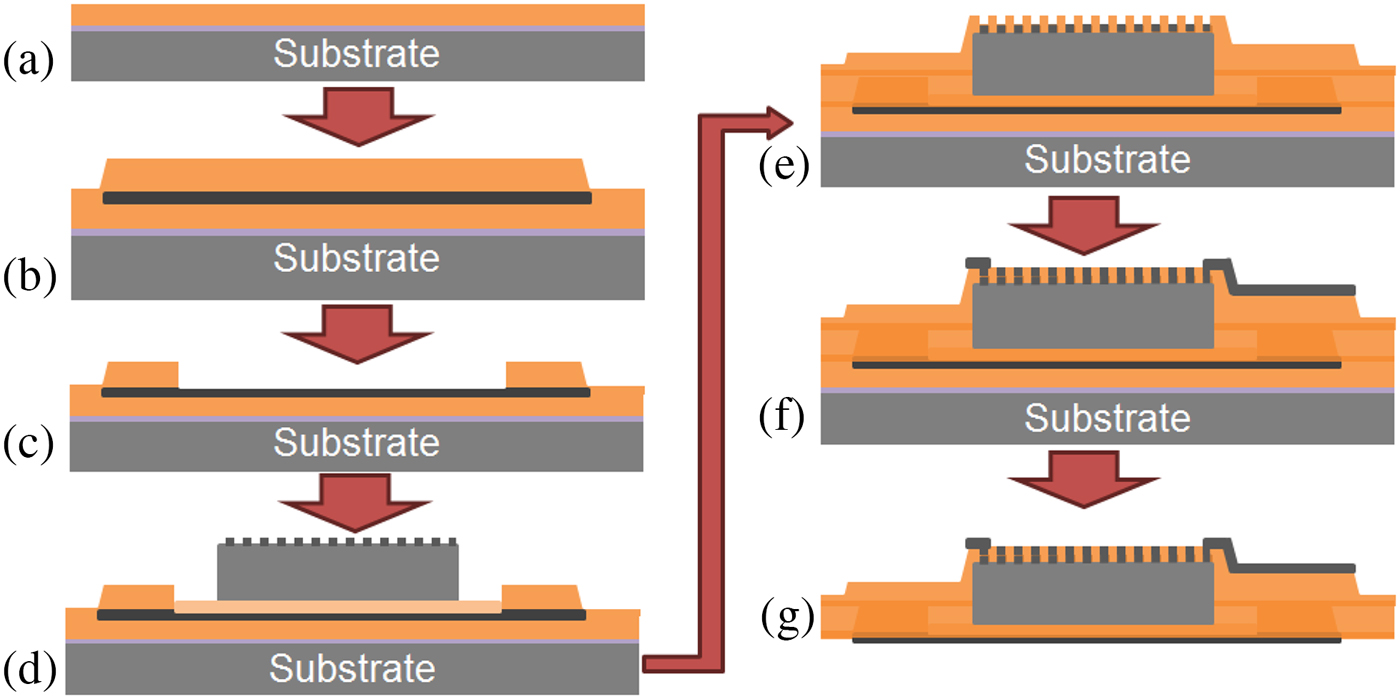
Firstly, a 10 μm polymer layer is spin coated and followed by sputtering 1.5 μm AlSiCu layer thickness. The heat spreader is then defined using lithographic step and metal etching. Then, a 5 μm polymer is spin coated and a cavity is defined by lithography and polymer plasma RIE. The thinned PA chip is placed and fixed in the cavity using 1 μm BCB (3000 series) as a permanent adhesive layer. After curing the BCB, the chip is covered with polymer and vias are opened using a hard mask and plasma etching. The vias are metalized and simultaneously an electrical fan-out is provided. After final metallization, the polymer on the backside of the heat spreader can be removed by plasma etching the backside of the released foil from the carrier. At the end of the process, the embedded chip inside polymer is released (see in Fig. 9) and further electrical measurements are performed. Despite the presence of the heat spreader, the bendability of the system is proven.
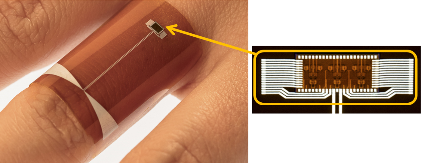
Demonstration of the embedded PA chip with the backside heat spreader in the CFP polymer foil. The integrated system-in-foil is released from the temporary silicon carrier and is bent over a cylinder with approximately 4 mm radius of curvature [Reference Alavi, Özbek, Rasteh, Grözing, Berroth, Hesselbarth and Burghartz16].

Electrical characterization
As described above, the thin PA chip is embedded inside the foil and connected to the flexible antenna on foil, showing mechanical flexibility (see in Fig. 10). RF performance of the amplifier and the antenna in the polymer foil are investigated separately.
Thin, flexible amplifier integrated circuit operating at 5.5 GHz, embedded in a flexible foil and connected to a broadband bowtie antenna [Reference Alavi, Özbek, Rasteh, Grözing, Berroth, Hesselbarth and Burghartz16].
3-path PA chip in the CFP
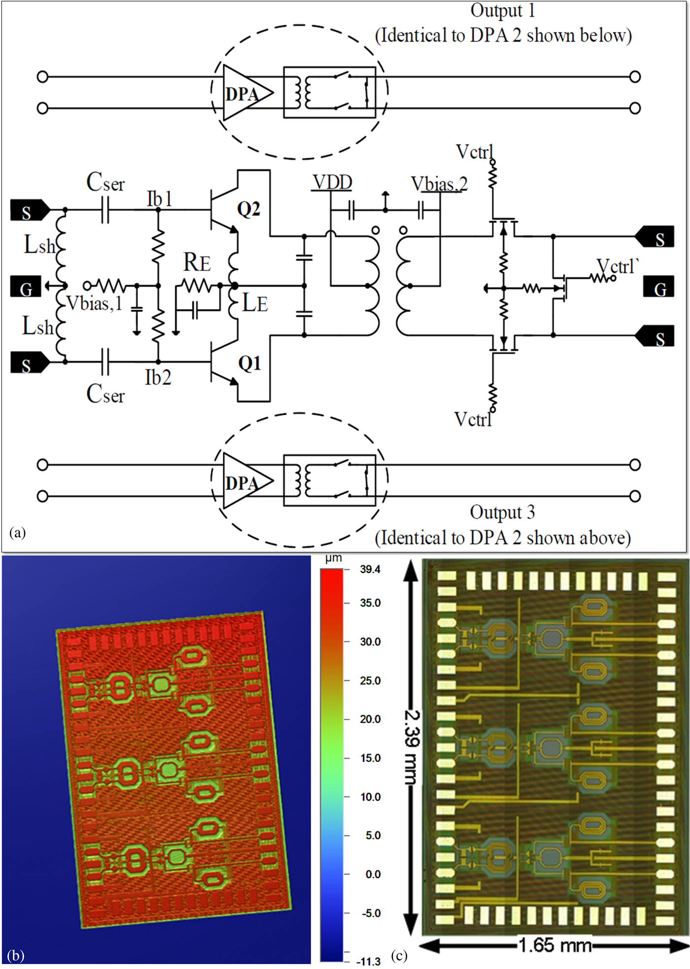
High-speed and cost-driven 95 GHz-fmax 0.25 μm-SiGe BiCMOS HBT technology is chosen, to keep the power consumption low within the required frequency band and avoid technology constraints. The simplified schematic view of the DPA is illustrated in Fig. 11. The fully integrated isolated NMOS switches with the topology of series/shunt configuration are intended to connect the PA array to a multi-feed antenna. All three amplifiers are identical to each other and a single path of a PA-array is investigated.
(a) Simplified schematic view of the DPA [Reference Özbek, Alavi, Digel, Grözing, Burghartz and Berroth14], (b) the measured surface topography of PA chip by using an optical profiler, and (c) the microscopic image of the PA chip.
RF performance of the amplifier has been evaluated with respect to the thickness of the substrate and the backside material in the previous study [Reference Özbek, Alavi, Digel, Grözing, Burghartz and Berroth14]. In this work, the embedded PA chip inside the CFP is measured and plotted in Fig. 12. The center frequency and gain are changing depending on the substrate thickness and the material below the IC. However, a minor S-parameters degradation after embedding the PA in the CFP foil (with/without heat spreader) is observed because of the broadband matching at the output.
Simulated and measured magnitude of S21 of the embedded PA chip in the CFP polymer foil.
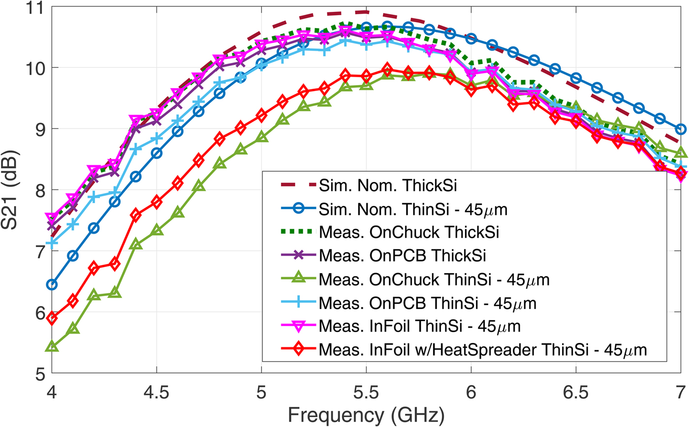
The measured center frequency on the thin silicon with backside metallization is shifted about 300 MHz toward higher frequencies compared to the thick silicon due to the image eddy currents within the conducting material. The inductors and transformer on thin Si chip (thickness of 45 μm) with the backside conducting material have slightly lower inductance due to the ground image mirror currents within the ground plane and accordingly degrading quality factor. In this study, conducting materials are a vacuum chuck and a heat spreader. Image of passive devices within the conducting material contributes a negative mutual inductance because the current flow in the return path is opposite direction. On the other hand, there is not much difference on the dielectric material (PCB) and foil, since they have a much higher resistance than the silicon substrate.
This measurement result matches to the simulated frequency shift of 200 MHz with a thin silicon substrate on the perfect electrical conductor (PEC). To improve the accuracy of the post-layout simulation and investigate the impact of the substrate thickness, all passive components except capacitors are extracted in one view and the image of the passive devices in the ground plane is considered by using a full-wave electromagnetic simulator (ADS-Momentum EM simulator).
In addition, according to the large signal measurements on the vacuum chuck, the PA output power at 5.5 GHz is 9 dBm before thinning and 8.1 dBm after thinning for an input power of − 1.3 dBm [Reference Özbek, Alavi, Digel, Grözing, Burghartz and Berroth14]. At the same input power and frequency, the embedded PA chip inside the CFP has 8.9 dBm output power without a heat spreader and 8.2 dBm output power with a heat spreader. The simulated output power at the 1 dB compression point is 10.8 dBm with a PAE of 15% at 5.5 GHz. The RF performance of the PA is measured by using a VNA with 0 dBm maximum output power. Hence, PA saturation is prevented.
Antenna characterization in the CFP
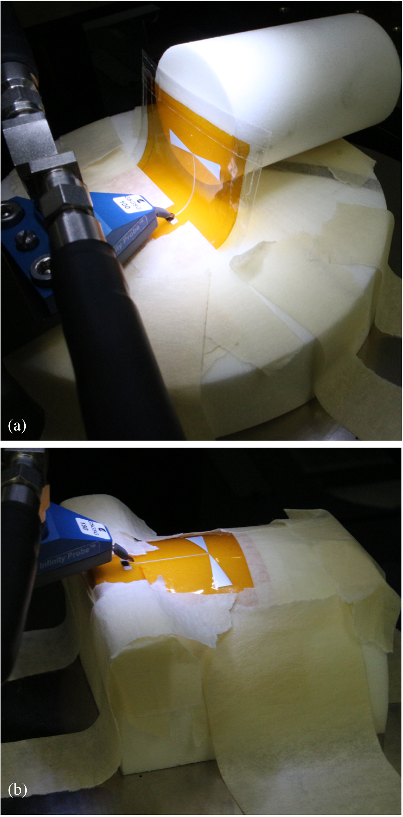
The fabricated antenna with the carrier frequency at 6 GHz on top of the polymer foil is measured as a stand-alone system. Therefore, each antenna is measured after releasing, straight, and on bent status with different radii of curvature (R). The measurements are performed using a vector network analyzer (VNA) (see in Fig. 13).
Graphical illustration of the bowtie antenna measurement on the polymer foil using VNA, (a) measurement as a straight bowtie, (b) measurement during bent status.
Antenna measurement result:
In this part, the antenna measurement setup in straight (see in Fig. 13(a)) and bent profile (see in Fig. 13(b)) is described. In order to decrease the measurement errors caused by metallic chuck in the probe station, a Rohacell chuck (εr ≈ 1) with a thickness of 20 mm is produced and the antenna is placed on it. As shown in Fig. 13(a), the antenna placed parallel to the Rohacell cylinder and the end of the feed lines is bent close to the GSGSG pads. In this way, the antenna functionality in the straight profile is measured. In addition, to measure the antenna in bent profile, the prototype is bent perpendicular to the antenna's main axis (see in Fig. 13(b)).
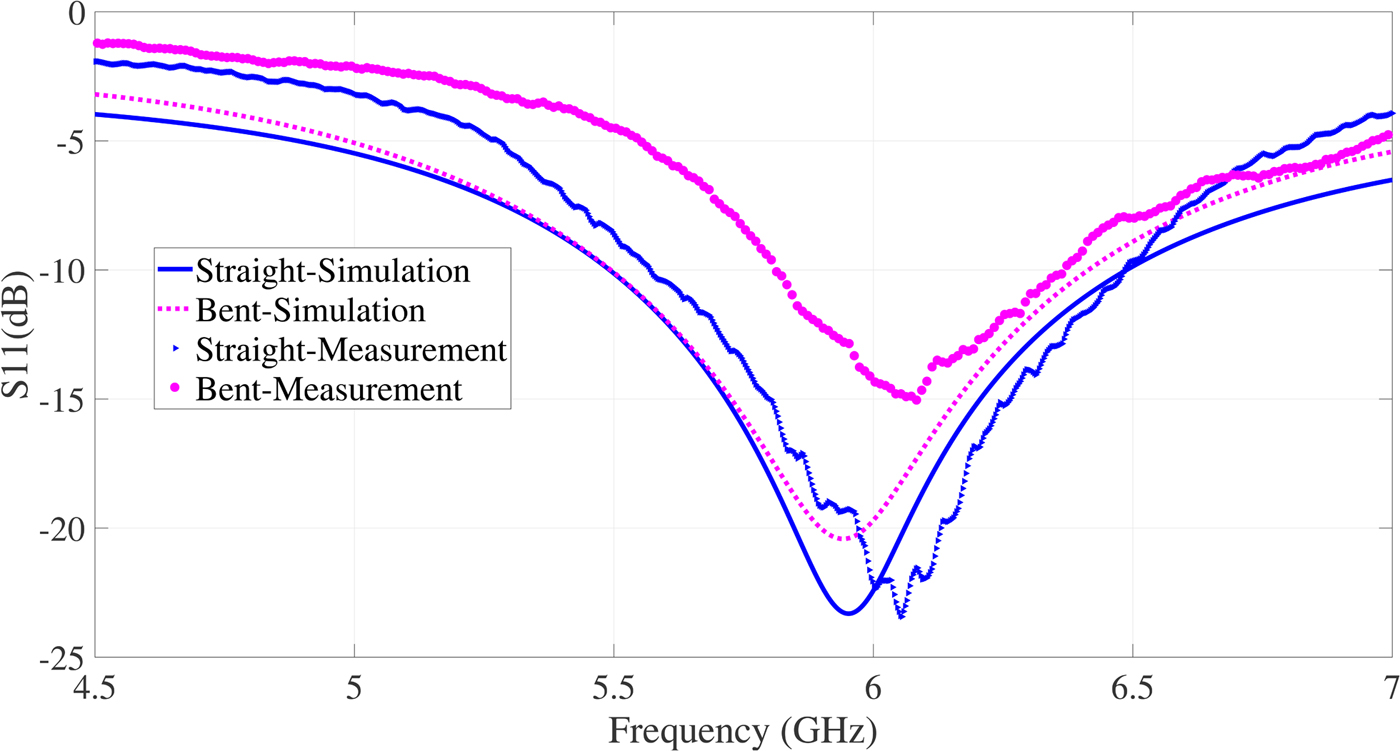
The simulated and measured result of the antenna input reflection magnitude is depicted in Fig. 14. There is a good agreement between measurement and simulation result of the antenna and the small shift in measured resonance frequency could be due to uncertainty in material parameters (thickness and electrical properties) of the substrate and metal layers used in the simulation. In Fig. 14, the simulated reflection coefficient of the antenna for straight and bent (R = 16 mm) profile versus the measured reflection coefficient of the antenna is shown. The bent antenna has measured the reflection coefficient of − 15 dB at the resonance frequency.
The reflection coefficient of the antenna in the bent and straight profile.
The thickness of the antenna is currently limited to 2 μm AlSiCu to follow CFP CMOS compatible fabrication technology. Unlike the feed impedance measurements with a wafer probe, the measurements of antenna radiation characteristics in straight and bent state require reliable connectors on the polymer foil. Then, balun circuit and cables can be connected for measurements in an anechoic chamber. For that means, a glued connection on thin AlSiCu was not successful. As a possible alternative, the use of solderable Silver for fabrication of the antenna on the polymer foil is suggested.
Conclusion
The thin silicon chip can be embedded and interconnected with a large-area antenna by using the high-frequency compatible two-polymer Chip-Film Patch technology. With the help of adaptive layout technique, proper design, and fabrication of heat spreader underneath the embedded chip, a PA chip with 75 mW power can be integrated in a CFP foil component while ensuring bendability and adequate power dissipation. The hybrid system including PA chip and on-foil antenna can operate at 6 GHz. As a part of the future work, a multiple feed antenna can be proposed.With a clever choice of the feed position on a multiple feed dipole antenna, the worst-case impedance mismatch can be minimized while the antenna is placed on the various environments with diverse permittivities. Additionally, the performance of the antenna is going to be compared based on the use of different fabricating materials (AlSiCu versus Silver). Ultimately, the complete system including multiple feed antenna and transmitter in the flexible CFP will be demonstrated.
Acknowledgments
We greatly acknowledge the contribution of all our teammates in IMS clean room, particularly Dr. Björn Albrecht, Dr. Christine Harendt, and Elisabeth Penteker. This work is supported by Deutsche Forschungsgemeinschaft (DFG) the FFLexCom-Project with grant-no. BE 2256/25-1.
 Golzar Alavi received her B.Sc. degree in electrical and electronics engineering from the Amirkabir University of Tehran in 2009. After finishing her M.Sc. degree at the University of Darmstadt with a focus on information and communication engineering, she is now pursuing her Ph.D degree at IMS CHIPS and the University of Stuttgart in the field of ultra-thin chip embedding and integrating in the polymer foil to develop complex hybrid system-in-foil (HySiF).
 Sefa Özbek was born in Istanbul, Turkey, in 1983. He received the B.Sc. degree in electrical engineering from the Fatih University, Istanbul, Turkey, in 2007 and the M.Sc. degree with a focus on electronics engineering fromthe University of Stuttgart, Stuttgart, Germany, in 2012. Since 2015, he has been pursuing the Ph.D. degree at the Institute of Electrical and Optical Communication Engineering, University of Stuttgart. His research interests include the design of front-end transceiver components in SiGe BiCMOS for IoT applications. Sefa Özbek worked as an IC design engineer with DMCE, Linz, Austria, from 2012 to 2015.
 Mahsa Rasteh received her B.Sc. degree in electrical and electronics engineering from the Urmia University in 2010. After finishing her M.Sc. degree at the University of Darmstadt with a focus on microwave engineering, she is now pursuing her Ph.D degree at the Institute of Radio Frequency Technology of Stuttgart University. Her current research area focuses on multiple feeds adaptive antenna.
 Markus Grözing received the Dipl.-Ing. and the Dr.-Ing. degrees from the University of Stuttgart in 2000 and 2007, respectively. During his doctoral study, his research was focused on phase noise and jitter in ring oscillators and on mixed-signal CMOS circuit design. Since 2007, he leads the integrated circuit design group at the Institute of Electrical and Optical Communications Engineering at the University of Stuttgart.
His current research topics are high-speed transmitters and receivers for serial links as well as gigasample-range analog-to-digital and digital-to-analog converters in CMOS and BiCMOS technologies. He has authored or co-authored more than 70 scientific papers and he has served as a reviewer for IEEE TMTT, JSSC, TCAS-II, JLT and TVLSI.
 Manfred Berroth was born in Obersontheim, Germany, in 1956. He received the Dipl.-Ing. degree from the University of the Federal Armed Forces, Munich, Germany, in 1979 and the Ph.D. (Dr.-Ing.) degree from Ruhr-Universität Bochum, Bochum, Germany, in 1991. In 1987, he joined the Institute for Applied Solid State Physics, Freiburg, Germany, where he was engaged in the development of circuit simulation models for GaAs field-effect transistors, as well as integrated circuit design. In 1995, he became the Deputy Director of the Institute for Applied Solid State Physics, Freiburg, Germany. Since 1996, he is a Full Professor and the Head of the Institute of Electrical and Optical Communication Engineering, University of Stuttgart, Stuttgart, Germany. He is a Treasurer of the IEEE Electron Devices Society Chapter Germany. His research interests are modeling and characterization of electronic and opto-electronic devices and integrated circuits.
 Jan Hesselbarth was born in Dresden, Germany, in 1970. He received the doctorate degree from Swiss Federal Institute of Technology (ETH), Zurich, Switzerland, in 2002. Jan Hesselbarth worked as a design engineer with Huber+Suhner, Switzerland, from 2001 to 2005, and as a member of technical staff with Bell Labs, Dublin, Ireland, from 2005 to 2008. He then joined ETH Zurich as a senior researcher and lecturer. Since 2011, Jan Hesselbarth is a professor at the Institute of Radio Frequency Technology at the University of Stuttgart, Germany. His research interests are in antennas and millimeter-wave circuits and packaging.
 Joachim N.Burghartz (M90SM92F02) received the Dipl.-Ing. and Ph.D. degrees in electrical engineering from RWTH Aachen, Aachen, Germany, and the University of Stuttgart, Stuttgart, Germany, in 1982 and 1987, respectively. He is the director of the Institute for Microelectronics Stuttgart (IMS CHIPS), and a full professor and head of the Institute for Nano and Microelectronic Systems (INES) at the University of Stuttgart. He also acts as the CEO of the IMS Mikro- Nano Produkte GmbH. Prof. Burghartz has published more than 350 peer-reviewed papers in technical journals and conference proceedings and holds more than 20 patents. He served in various functions within the IEEE Electron Devices Society (EDS) and he is the recipient of the 2014 J. J. Ebers Award of the IEEE EDS.


 Open access