
Introduction
Electron beams of the large cross-section (102–104 cm2) extracted through foil windows into the air or high-pressure gas are used for excitation of high-power lasers, polymerization of monomers, switching of high currents, sterilization of foodstuffs and medical tools, air and water purification, plasma chemistry, radiation chemistry, and so on. (James, Reference James1979; Bugaev et al., Reference Bugaev, Kreindel and Schanin1984; Sokovnin, Reference Sokovnin2007; Vorob'ev et al. Reference Vorob'ev, Denisov, Koval’, Shugurov, Yakovlev, Uemura and Raharjo2015]. Often, one of the major problems in sources of such beams is to minimize the energy loss of a beam during its formation, transport, and extraction.
The Institute of High Current Electronic SB RAS (Tomsk, Russia) develops electron sources based on a low-pressure arc with a mesh plasma cathode (Gielkens et al., Reference Gielkens, Peters, Witteman, Borovikov, Stepanov, Tskhai, Zaivjalov, Guschenets and Koval1996; Grigoryev et al., Reference Grigoryev, Koval, Devjatkov, Teresov and Schanin2008; Vorob'ev et al., Reference Vorob'ev, Gamermaister, Devyatkov, Koval’, Sulakshin and Shchanin2014; Vorobyov et al., Reference Vorobyov, Koval and Sulakshin2015a, Reference Vorobyov, Devyatkov, Koval and Shugurovb, Reference Vorobyov, Koval, Sulakshin and Shugurovc) which find application in unique facilities of Russia [http://ckp-rf.ru/usu/434216]. The use of the arc discharge for the generation of emission plasma provides high energy efficiency of such electron sources as the average discharge power is no greater than 100 W at an average beam power of up to several kilowatts, and the mesh-stabilized emission boundary allows one to independently control the beam parameters (electron energy, beam current, pulse repetition frequency) and vary them over a wide range.
Here we present experimental and theoretical data on the plasma characteristics, electron beam parameters, and main energy loss mechanisms in a wide-aperture electron accelerator based on a low-pressure arc with a mesh plasma cathode.
Experimental setup and measurement methods
The generation, transport, and an electron beam extraction into the air were studied on an accelerator with a multi-aperture mesh plasma cathode based on the low pressure arc (Vorobyov et al., Reference Vorobyov, Koval and Sulakshin2015a, Reference Vorobyov, Devyatkov, Koval and Shugurovb, Reference Vorobyov, Koval, Sulakshin and Shugurovc). Its simplified schematic and photo are presented in Figures 1 and 2, respectively. The accelerator provides the formation of a cross-section electron beam (750 × 150 mm2) in repetitive pulsed modes with the following maximum beam parameters (not at the same time): electron energy 200 keV, beam current in air 30 A, pulse duration 100 µs, and pulse repetition frequency 50 Hz.
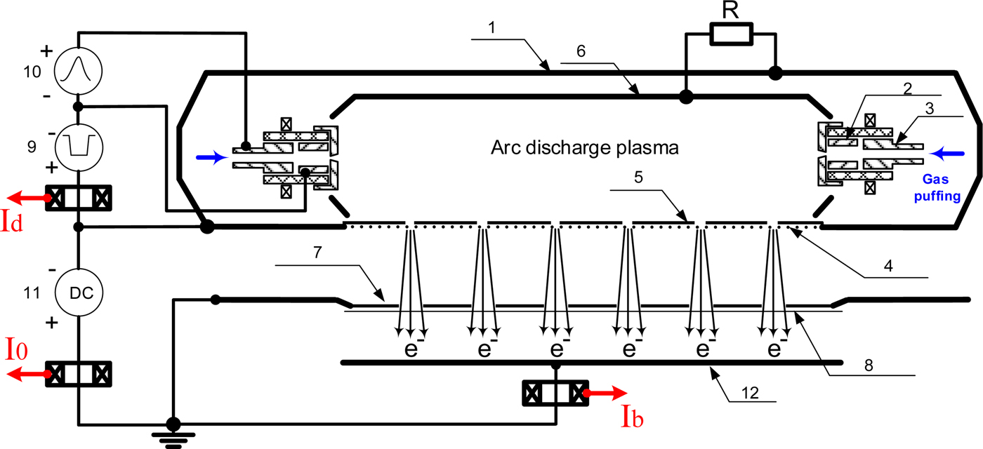
Schematic of the electron accelerator: 1 – plasma cathode; 2 – metal cathode; 3 – igniter; 4 – emission mesh; 5 – mask; 6 – hollow anode; 7 – support grid for output foil; 8 – output foil; 9 – discharge power supply; 10 – igniter power supply; 11 – high-voltage power supply; 12 – collector or substrate.
DUET electron accelerator.

In the accelerator (Fig. 1), plasma cathode 1 is a hollow stainless steel semi-cylinder of dimensions 200 × 150 × 800 mm3 at the ends of which there are two cathode units based on a low-pressure arc with a cathode spot initiated by an electrical breakdown of the working gas (Vorobyov et al., Reference Vorobyov, Koval and Sulakshin2015a, Reference Vorobyov, Devyatkov, Koval and Shugurovb, Reference Vorobyov, Koval, Sulakshin and Shugurovc).
The inner surface of the semi-cylinder serves as hollow anode 6 for two cathode units. Emission mesh 4 of dimensions 750 × 150 mm2 is covered with stainless steel mask 5 of thickness 200 µm (Fig. 3a) having 344 holes of diameter 8–12 mm. Each section of the mesh bounded by a hole in the mask is individual emission elements of the mesh plasma cathode. Hollow anode 6 is connected to emission mesh 4 via resistance R to provide switching of the discharge current to the emission region. For electron extraction from the emission surface, an accelerating dc voltage of up to U 0 ≤ 200 kV is applied between the plasma cathode 1 and output foil window 7,8 of the accelerator. The accelerating gap is d = 140 mm. The output foil window (Fig. 3b) comprises support Cu grid 7 of thickness 20 mm and output Al–Mg foil 8 of thickness 30 µm which provides extraction of electrons with energies E 0 ≥ 80 keV (Seltser & Berger, Reference Seltser and Berger1974). The support grid has a total geometric transparency of 56%. The number of coaxial holes in the support grid is the same as that in the mask but their diameter is larger (15 mm). Thus, the broad electron beam represents a superposition of elementary beams formed by individual emission elements whose plasma boundary is stabilized by the fine metal mesh.
Spot-welded mask on emission mesh (a) and output foil window (b).

The discharge current I d, current in the accelerating gap I 0, and beam current I b extracted into the air were measured with Rogowski coils in the respective circuits (Fig. 1). The beam current I b was measured with Al collector 12 of dimensions 800 × 200 mm2 located in the air at 20 mm from the output foil.
Experimental and theoretical research
The multi-aperture two-electrode electron-optical system has allowed us to increase the accelerator efficiency by increasing the beam extraction factor β = I b/I 0. Of significance is that our estimates of I b (Fig. 4a) take into account the reflection of accelerated electrons from the collector, as opposed to data reported elsewhere (Vorobyov et al., Reference Vorobyov, Koval and Sulakshin2015a, Reference Vorobyov, Devyatkov, Koval and Shugurovb, Reference Vorobyov, Koval, Sulakshin and Shugurovc). Decreasing the beam current loss has made it possible to increase the average output beam power from 2.5 kW to more than 4 kW and thus to bring the accelerator to a new technological level. The further increase in the average beam power was limited by the maximum output power of the high-voltage power supply.
Beam extraction efficiency β versus accelerating voltage U 0 and beam pulse duration t at U 0 = 200 kV (a) with no mask (1, 3) and with it (2, 4) and electron extraction efficiency α versus U 0 with mask holes of diameter 8 mm and mesh width h = 0.6 mm (b).
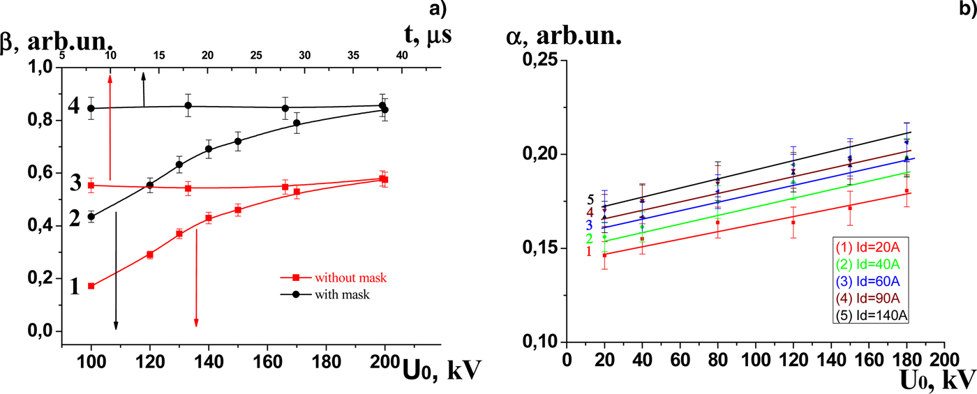
Previously (Vorobyov et al., Reference Vorobyov, Koval and Sulakshin2015a, Reference Vorobyov, Devyatkov, Koval and Shugurovb, Reference Vorobyov, Koval, Sulakshin and Shugurovc), it was also reported that decreasing the mask hole diameter, that is, the electron emission area, can provide higher values of β and more stable operation of the mesh plasma cathode. However, this decreases the electron extraction factor α = I 0/I d. As can be seen from Figure 4b, the factor α depends on the accelerating voltage U 0 and on the emission plasma density n e which increases with I d. It is also obvious that α increases with h. Based on the work of (Oks, Reference Oks2006) let us consider these phenomena at greater length.
For analyzing the discharge plasma characteristics (plasma density, electron temperature, plasma potential), we can use a numerical model which describes the density of plasma electrons n e = n i and their average energy n ε as a function of space and time (Hagelaar & Pitchford, Reference Hagelaar and Pitchford2005):
 $$\displaystyle{{\partial n_{{\rm e},{\rm \varepsilon}}} \over {\partial t}} + \nabla \vec {\rm \Gamma} _{{\rm e},{\rm \varepsilon}} = R_{{\rm e},{\rm \varepsilon}}, \quad \vec {\rm \Gamma} _{{\rm e},{\rm \varepsilon}} = - D_{{\rm e,{\rm \varepsilon}}} \cdot \nabla n_{{\rm e},{\rm \varepsilon}}. $$
here Γe,ε is the electron and energy flux; μe,ε is the electron mobility and energy; D e,ε is the diffusion coefficient; and R e,ε is the rate of ionization and change of electron energy due to inelastic collisions dependent on the electron energy distribution function. Model (1) ignores the processes in the collisionless electric double layer between the discharge column and target; the input data (electron flux and energy) are determined from experiments. The plasma potential with respect to the emission electrode is estimated by the formula:
 $${\rm \varphi} = \displaystyle{{kT_{\rm e}} \over e} \cdot \ln \left( {2\displaystyle{{1 + r} \over {1 - r}}} \right),$$
where k is Boltzmann's constant, е and T e are the electron charge and its temperature, r is the electron reflection coefficient from the computational domain boundary.
As the experiment suggests, increasing the resistance R decreases the current rise time in the accelerating gap such that at R ≥ 10 Ω the current I 0 takes a more stable shape with a clearer flat peak, reproducing the discharge current I d. The effect of R on the discharge plasma parameters was analyzed numerically using model (1) with R taken as the electron reflection coefficient r from the anode surface and with the electron current to the anode cavity I a(r) corresponding to experimental I a(R).
For the total mesh transparency ≈45% (cell width h = 0.4 mm) without mask 5 (Fig. 1), the electron extraction factor α from the plasma cathode to the accelerating gap of width d = 140 mm reaches its maximum value at R ≥ 10 Ω in the anode circuit (Fig. 5a) and remains almost constant with further increasing the resistance R. As already noted, the factor α increases with increasing the discharge current and accelerating voltage, which is due to a penetration of the electric field from the accelerating gap to the space of the plasma cathode through cells of the emission mesh when the electron component of the discharge current takes the path through the circuit of the high-voltage power supply (Oks, Reference Oks2006). From Figure 5a it is seen that this method of current switching is very efficient and provides a near two-fold increase in the electron extraction factor α for almost no change in the discharge operating voltage U d (Fig. 5b).
Electron extraction factor α (a) and discharge operating voltage Ud (b) versus resistance R in experiments with no mask at U 0 = 160 kV, h = 0.4 mm, and d = 140 mm for I d equal to 20 A (1), 40 A (2), 60 A (3), 90 A (4), 100 A (5), and 150 A (6).

Figure 6 presents experimental curves for the hollow anode current I a as a function of R and calculated curves for the plasma density n e and plasma potential φ with respect to the anode at I d = 100 A and I d = 20 A. The calculations show that increasing the resistance R from 0 to 10 Ω allows to increase the plasma density n e and plasma potential φ. This is because the fraction of electrons reflected from hollow anode walls increases, the number of their interactions with the working gas grows, and this increases the density of chaotic current and hence the emission current.
Experimental curves for anode current I a (1, 2) and respective calculated curves for plasma density n e (3, 4) and plasma potential φ (5, 6) with respect to anode as a function of R at I d = 20 A (1, 3, 5) and 100 A (2, 4, 6).

From the calculations, it follows that the saturation of α at R > 10 Ω (Fig. 5a) is most likely due to near-total reflection of plasma electrons from the anode. The continuity of the current, in this case, is provided by fast electrons which are accelerated in the region of cathode potential fall and reach the hollow anode with minimum energy loss.
Thus, the discharge current in the plasma cathode is determined by the following components: the current of fast electrons I eb not participating in the gas ionization into the plasma cathode, the electron current to the metal surface of the hollow anode and emission mesh, and the emission current through the potential barrier Δφ = φf(r)– DU 0(z pl) (Oks, Reference Oks2006):
 $$I_{\rm d} = I_{{\rm eb}} + j_{{\rm ch}}S_{\rm a}\ell ^{ - \displaystyle{{e{\rm \varphi}} \over {kT_{\rm e}}}} + j_{{\rm ch}}S_{\rm f}\ell ^{ - \displaystyle{{e{\rm \varphi} _{\rm f}} \over {kT_{\rm e}}}} + j_{{\rm ch}}S_{\rm e}\ell ^{ - \displaystyle{{e{\rm \Delta} {\rm \varphi}} \over {kT_{\rm e}}}}.$$
Here S a and S f are the metal surface areas of the hollow anode and emission mesh; S e is the cell area of the emission mesh; φf is the plasma potential with respect to the emission electrode; U 0 is the accelerating voltage in the diode; j ch is the chaotic current density; DU 0(z) is the accelerating field which penetrates in the plasma cathode through mesh cells and is approximated by the formula:
 $$DU_0(z) = c_1\displaystyle{{hU_0} \over {2d}}\exp \left( { - 2c_2\displaystyle{{{\rm \rho} - z} \over h}} \right).$$
Here D is the coefficient of electrical permeability of the emission electrode, c 1, c 2 are constants dependent on the mesh transparency, h is the cell width, ρ is the mesh wire diameter, and d is the length of the accelerating gap.
Assuming for simplicity that I eb ≈ 0 in (3), the expression for the electron extraction factor α takes the form:
 $${\rm \alpha} = \left[ {e^{ - \displaystyle{{{\rm \Delta} {\rm \phi}} \over {kT_{\rm e}}}}} \right]\left[ {\displaystyle{{S_{\rm a}} \over {S_{\rm e}}}e^{ - \displaystyle{{e{\rm \phi}} \over {kT_{\rm e}}}} + \displaystyle{{S_{\rm f}} \over {S_{\rm e}}}e^{ - \displaystyle{{e{\rm \phi} _{\rm f}} \over {kT_{\rm e}}}} + e^{ - \displaystyle{{e{\rm \Delta} {\rm \phi}} \over {kT_{\rm e}}}}} \right]^{ - 1}$$
The plasma potential φ and the plasma density n e increase simultaneously with R (Fig. 6). From expressions (3) and (5) it follows that increasing the plasma potential φ decreases the current to the hollow anode I a and increases the current in the accelerating gap, which increases the extraction factor α.
When a change occurs in the plasma potential φf or in the accelerating voltage U a, it changes the position of the plasma emission boundary. The position of the boundary is determined from the condition of equality of the electrostatic pressure in the accelerating gap ε0E2/2 and the kinetic pressure of the plasma n ekT e (Oks, Reference Oks2006), where ε0 is the dielectric constant and E is the electric field strength in the accelerating gap, with the plane z pl = 0 coincident with the emission mesh plane from the side of the plasma cathode:
 $$z_{{\rm pl}} = {\rm \rho} \left[ {1 - \displaystyle{h \over 2}c_2\ln \left( {\displaystyle{{c_1c_2U_0} \over {dE}}} \right)} \right]$$
when electrons are emitted through the potential barrier (z pl < 0 or h/2 < l i , where l i is the thickness of the positive space charge layer separating the plasma from the emission electrode), the emission mesh stabilizes the plasma boundary as long as the increase in the emission current is compensated by the increase in the plasma potential, provided that φf(r) > DU 0(z pl) and the potential φf(r) does not exceed the breakdown potential (mesh electrode – discharge plasma) (Burdovitsin et al., Reference Burdovitsin, Kuzemchenko and Oks2002; Oks, Reference Oks2006; Gavrilov et al., Reference Gavrilov, Emlin and Kamenetskikh2008; Devyatkov & Koval, Reference Devyatkov and Koval2014).
In addition, calculations were performed to study the influence of the emission surface area on the plasma parameters. For simplicity, the mask was represented as a uniform rectangular mesh structure on the emission mesh surface (Fig. 7). Figure 8 shows experimental and calculated curves for the emission current I em as a function of S mask/S mesh, where S mask is the mask surface area and S mesh is the mesh surface area. The calculations suggest that as the ratio S mask/S mesh is increased from 0 to 0.5, the plasma density increases by 36% with slight variations in the plasma temperature T e and potential φf and the layer thickness l i decreases by ≈15%: l i = r D(eφf/kT e)3/4, where r D = (ε0kT e/e2n e)1/2 is the Debye radius. Thus, the increase in R and the use of the mask on the mesh create an electrostatic trap which increases the number of electrons reflected from the inner walls of the hollow anode, mask, and mesh wires.
Mask geometry in calculations and experiments.

Current in the accelerating gap I 0 as a function of S mask/S mesh at U 0 = 200 kV, h = 0.6 mm in calculations (1, 3) and experiments (2, 4) for I d = 20 A (1, 2), 90 A (3), and 100 A (4).

Our experiments show that without mask at d = 140 mm and h = 0.6 mm, the operation of the electron accelerator is unstable. The currents I d and I 0 reveal high-frequency modulations at about 1–2 MHz and the accelerating voltage starts influencing the shape and amplitude of the discharge current. This eventually decreases the electric strength of the accelerating gap (in terms of breakdowns per 1000 pulses of beam current) and the operation stability of the plasma cathode power supply up to the failure of its circuit elements. The use of a mask in the emitter eliminates all high-frequency modulations on the oscillograms of I d and I 0 and the influence of the accelerating voltage on their shape and amplitude.
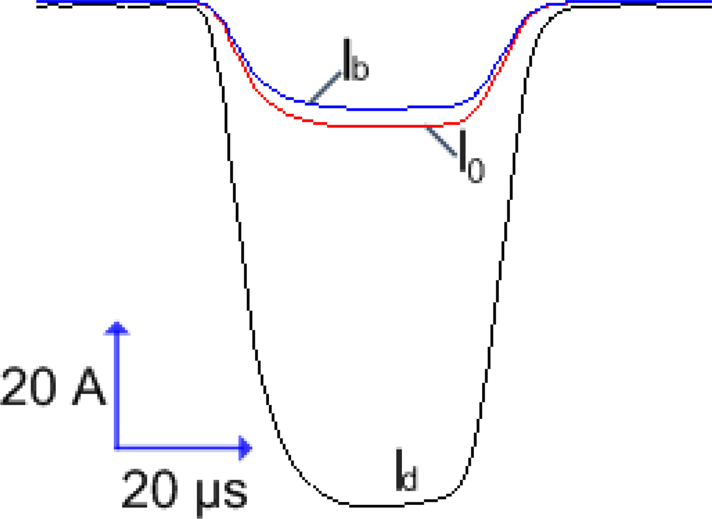
Figure 9 shows typical waveforms for I d and I 0 at U a = 150 kV with mask holes of diameter 8 mm, geometric transparency 13%, and mesh width h = 0.6 mm. Figure 10 presents calculation data demonstrating how the plasma density n e varies with time t along the longitudinal axis of the plasma cathode at the emission mesh surface. Our experiments suggest that even without additional measures, for example, the use of a mask with variable geometric transparency (Vorob'ev and Koval Reference Vorob'ev and Koval’2016), the plasma density nonuniformity is no greater than 15% and the beam extraction factor β remains constant throughout the beam current pulse (see Fig. 4).
Typical waveforms of discharge current I d, current in accelerating gap I 0, and extracted beam current I b at U 0 = 200 kV with mask holes of diameter 8 mm, geometric transparency 13%, and h = 0.6 mm
Calculated variation of plasma density n e with time t along the longitudinal axis of plasma cathode at emission mesh surface (Fig. 7, line L).

The beam current loss can be caused by the following main factors: (1) imperfect alignment of holes in the mask and support grid; (2) defocusing of the beam due to Coulomb repulsion of particles and electric field inhomogeneity in the region of emission holes; (3) scattering of electrons during their acceleration at atoms of the working gas, residual gas, and gas desorbed from the electrodes; (4) reflection of high-energy electrons from the output foil and their oscillation in the accelerating gap with the least probability of their escape into air but with their participation in the ionization of the working gas, residual gas, and gas desorbed from the electrodes.
The scattering of electrons at atoms of these gases leads to their ionization and to the appearance of high-energy ions in the accelerating gap, which can also be considered as a beam energy loss because ion bombardment of the plasma cathode electrodes causes their heating and decreases the overall efficiency of the accelerator. Besides, such bombardment of the emission mesh and mask brings electrons in the accelerating gap due to ion-electron emission. The number of these electrons depends on the state and material of the plasma cathode electrodes and on the energy of bombarding ions, and the probability of their escape into air is low because of the difference in electron and ion beam trajectories starting from the emission structure of the plasma cathode and from the holes of the support grid respectively (Vorobyov et al., Reference Vorobyov, Koval and Sulakshin2015a, Reference Vorobyov, Devyatkov, Koval and Shugurovb, Reference Vorobyov, Koval, Sulakshin and Shugurovc).
Considering the balance of currents in the accelerating gap and ion-electron emission from the mask and grid surface, we analyzed the beam current loss I i/I 0 due to ion currents I i = I ib + I if, where I ib is the ion current due to bulk gas ionization by electrons emitted from the discharge plasma and electrons reflected from the output foil window and I if is the ion current due to ionization of the gas desorbed from the foil surface by fast beam electrons whose energy corresponds to accelerating voltage.
For beam electrons with an energy of 100 keV acting on the target surface, the gas desorption is m = 10 molecules/electron (Abdullin et al., Reference Abdullin, Bazhenov, Yerokhin and Ladyzhensky1985). The desorbed gas concentration near the target surface is n ag = m j0/ev a, where v a ≈ 6·104 cm/s is the velocity of an atom. The ion current density due to bulk ionization of the gas desorbed from the foil surface by beam electrons is j if = j 0σe i d(n g + n ag), where n g is the gas concentration, σei is the ionization cross-section. For the electron current density in the accelerating gap j 0~0.1 A/cm2, the desorbed gas concentration n ag = 1014 cm–3 is of order of magnitude higher than the working gas density in the gap n g = 1013 cm–3 (р = 0.04 Pa). Assuming σ ei~5·10–18 cm2, for example, for nitrogen (Moravej et al., Reference Moravej, Yang, Barankin, Penelon, Babayan and Hicks2006), the relative ion current density is j if/j 0~5·10–3 and its value due to bulk gas ionization by emitted and reflected electrons is j i/j 0~10–4. However, it should be noted that the ion current density increases greatly with increasing the gas pressure and electron reflection coefficient from the output window. Nevertheless, in our experiments, the beam current loss I i/I 0 due to ion currents is no greater than 1%.
The calculations demonstrate inessential effects of the processes associated with self-fields of elementary beams and bulk gas ionization by electrons accelerated in the diode. However, the electric field inhomogeneity in the region of emission holes (Fig. 11a) can influence the electron trajectories in the accelerating gap, eventually resulting in beam current loss at the support grid (Astrelin et al., Reference Astrelin, Burdakov, Grigoriev, Kandaurov, Koval and Teresov2010). Most of the influence on the angular distribution is due to edge effects of the mask (Fig. 11b) when its coverage of end cells is incomplete and its attachment to the mesh is loose. Figure 12 shows elementary electron and ion beam configurations obtained from numerical solutions of motion equations for electron emission from the plasma boundary z pl with statistically processed phase coordinates.
The potential in the near-grid region due to penetration of accelerating electric field (a) at U a = 100 kV (1) and 200 kV (2), and edge effects on angular electron distribution with loose mask-to-mesh attachment (b).
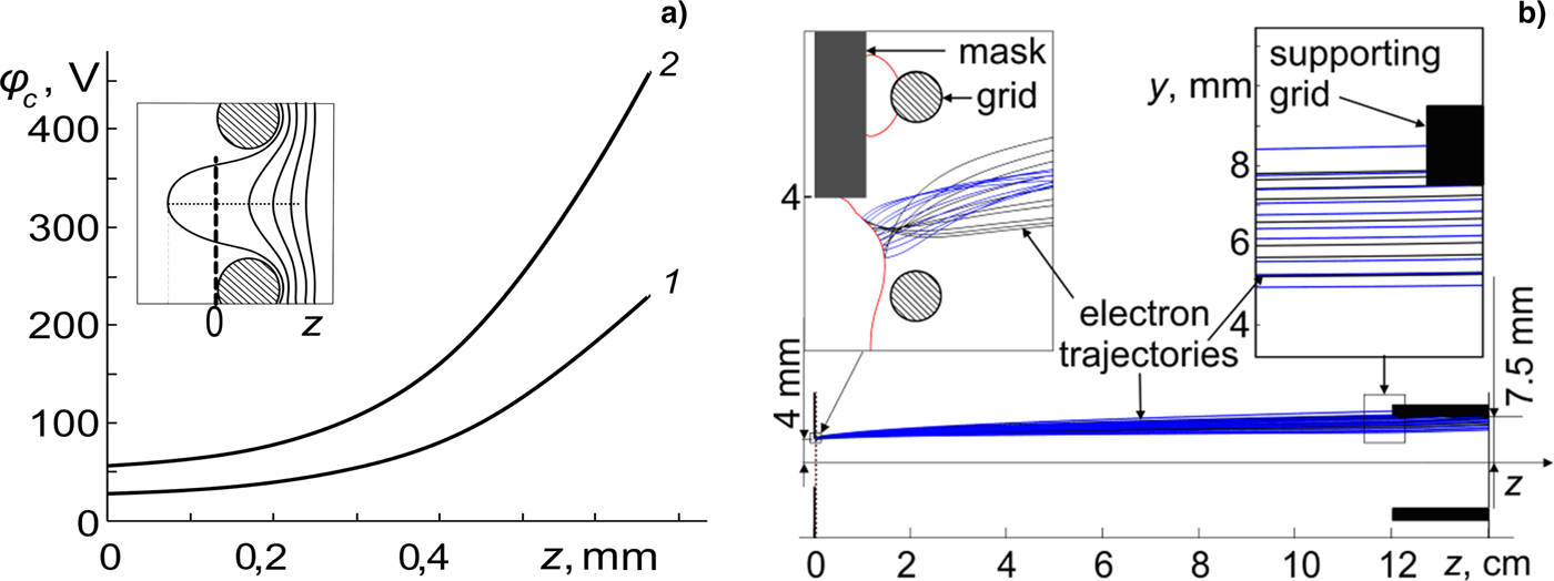
Elementary ion (a) and electron beam configurations (b) at U a = 200 kV, h = 0.4 mm, mask and support grid hole diameters 8 mm and 15 mm, respectively: 1 – emission mesh, 2 – mask, 3 – support grid, 4 – foil, 5 – discharge hollow anode.

In experiments, the spacing between the mask and the emission mesh can reach 1 mm, causing the area of the emitting plasma surface to increase somewhat such that electrons at the edges are angularly dispersed and fail to arrive at the support grid. Estimates show that for the spacing increased by 0.6 mm (cell width), the lost beam current can range to over 7%.
The electron and ion dynamics in the accelerating gap were studied using the PIC code KARAT (Tarakanov, Reference Tarakanov1992). Because the electric field inhomogeneity in the cell region is difficult to account for, the electrons in the emission plane were assigned initial angular and energy spreads according to the model considered above (Figs 11–12). Figure 13a shows the pattern of emitted and reflected electrons with velocity vectors (arrows) for their model distribution in the emission plane at which 10% of beam electrons with an energy of 70–150 eV have an entrance angle of 0°–75°. The loss of electrons depends strongly on their angular spread and on the mask hole diameter. For the mask hole diameter 8 mm, the beam current lost at the support grid with a hole diameter of 15 mm is ≈6%.
The pattern of emitted and reflected electrons (a) and calculated current density distribution in one hole of output foil window (b).

The calculations show that the loss of electrons at the support grid depends weakly on the accelerating voltage U 0 due to small variations in the transverse velocity of electrons arriving in the accelerating gap (Fig. 11). The main beam current losses with decreasing U 0 are related to losses in the foil (Fig. 4a): the beam current in the air is I b≈0.85·I 0 at U 0 = 200 kV and I b≈0.6·I 0 at U a = 130 kV, which agrees with data reported elsewhere (Seltser & Berger, Reference Seltser and Berger1974). According to theoretical estimates, the percent of electrons reflected from the output foil, in this case, is 3–4% of the total electron current arriving at the foil. It should be noted that the beam current loss can be contributed by a decrease in accelerating voltage during the beam current pulse and by fast electrons arising in the discharge plasma and arriving in the accelerating gap with high transverse velocities.
The two-electrode multi-aperture electron-optical system of the accelerator allows extraction of about 85% of the beam current and more than 70% of the beam power from the accelerating gap into the air (with regard to electrons reflected from the collector). The lower value of the beam power in the air compared with the beam current owes to accelerated electrons which lose part of the energy in the foil in their inelastic interactions with atoms of its lattice. In addition, the beam spends a few percent of the energy in gas heating when it passes the air gap of 2 cm between the foil and collector (Fig. 1), which also decreases the beam energy and greatly broadens its spectrum in the air (Kozyrev et al., Reference Kozyrev, Kozhevnikov, Vorobyov, Baksht, Burachenko, Koval and Tarasenko2015).
Conclusion
Our experiments and numerical simulation suggest that the use of a mask in the multi-aperture plasma cathode and resistance in the hollow anode circuit makes it possible to increase the emission plasma density by more than 30% and the electron extraction efficiency by a factor β of ≈2 times.
According to numerical estimates, the beam current loss at the support grid depends largely on the angular velocity spread of emitted electrons which is contributed by edge effects at the mask holes, nonuniform distribution of the electric field penetrating in the plasma cathode, and fast electrons universally present in the electron energy spectrum of the discharge. The numerical estimates also show that at an operating pressure of 40 mPa and beam current density of 0.1 A/cm2, the ion fraction in the total current in the accelerating gap is no greater than 1%. Noteworthy is that for the electrons resulting from ion-electron emission, the probability of escape into the air through the foil is very low. At U 0 = 200 kV, the beam current lost at the support grid can range to 7% and its loss in the output foil reaches 10%.
Elimination of the beam current loss at the support grid of the output foil window through accurate alignment of its holes with mask holes can provide a considerable increase in the efficiency and reliability of the electron accelerator, and this opens up new avenues for this type of sources in scientific and technological fields.
Acknowledgments
The work on this paper was supported by the Russian Science Foundation (project No. 14-29-00091).


