

Introduction
The ongoing development of GaN-based power amplifiers for higher P out and higher frequencies opens a growing market for wide-bandgap semiconductor devices [Reference Mishra, Parikh and Wu1,Reference Wu2]. Radio-frequency (RF) communication systems would extremely profit from this trend leading to even higher integration densities, smaller system sizes, and overall better system performance.
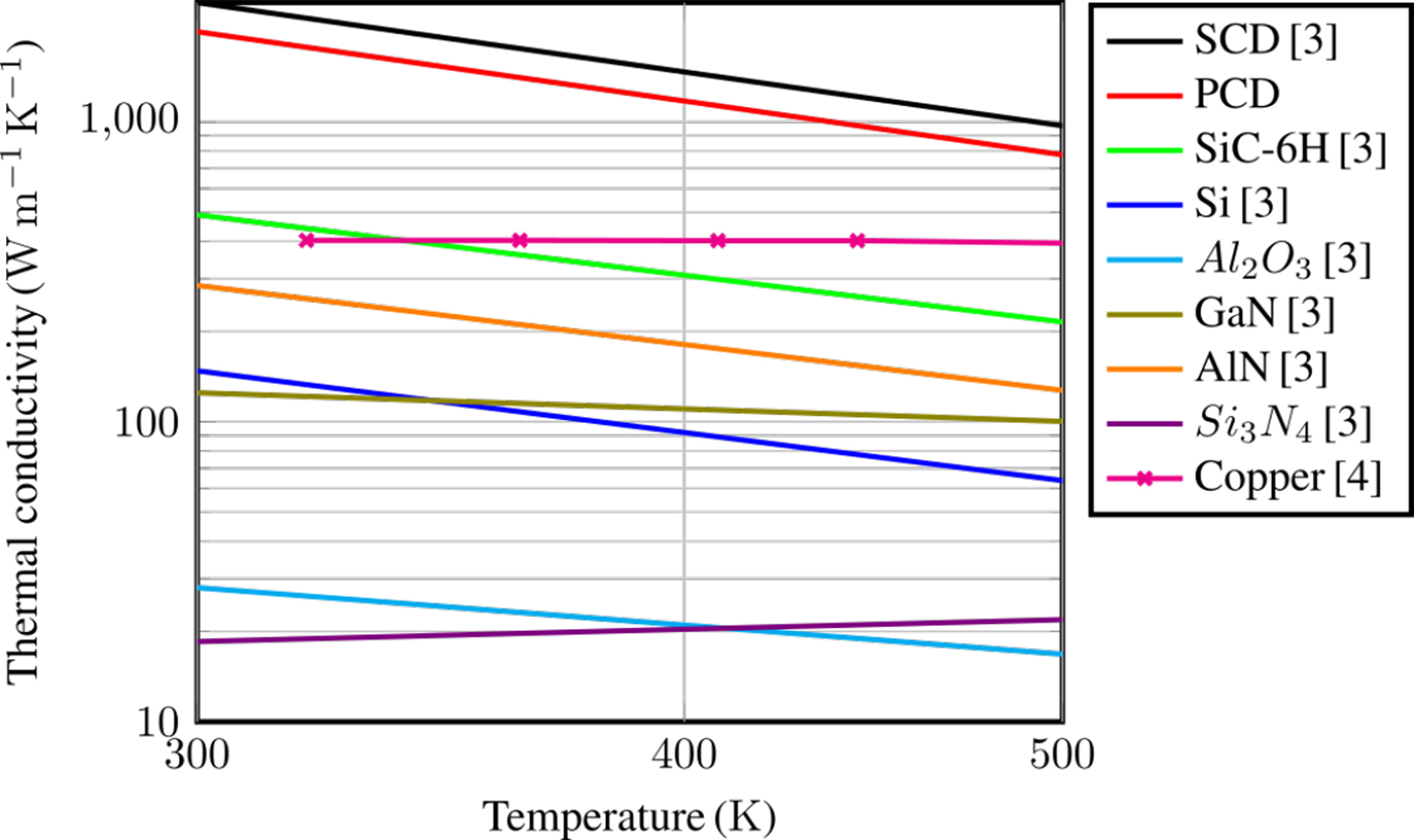
Due to the lack of large area GaN substrates, GaN devices are mainly fabricated on three different substrates: Silicon carbide (SiC), Si, and sapphire. GaN-on-SiC achieves currently the highest power densities attributed to its largest thermal conductivity. Despite extremely highradio-frequency (RF) power densities of 40 W mm−1 [Reference Wu2], thermal management is still the primary limiting factor. Diamond as substrate would provide four times higher thermal conductivity (κ diamond > 2000 W m−1 K−1) than SiC (κ SiC = 490 W m−1 K−1), which potentially allows even higher performance (see Fig. 1).
Temperature dependence of thermal conductivities for different substrates (SCD, PCD, Si, SiC-6H, and Al 2O 3) and AlGaN/GaN device specific materials (all from [Reference Palankovski and Quay3]) and copper [Reference Touloukian4].
Heterointegration of AlGaN/GaN layers on diamond as new substrate was realized by growth and by bonding. The growth of AlGaN/GaN on diamond, on bothpolycrystalline diamond (PCD) [Reference Webster5,Reference van Dreumel6] and SCD [Reference Hirama, Kasu and Taniyasu7–Reference Hageman, Schermer and Larsen9] usually suffers from a poor electronic quality of the AlGaN/GaN layers, which require careful interface control and stress engineering during the epitaxial growth and the final cool down. The reverse approach, the growth of diamond on AlGaN/GaN was demonstrated both on the top [Reference Anderson10] or the bottom [Reference Ejeckam11] of the GaN layer and already competes with the GaN-on-SiC technology [Reference Blevins and Via12,Reference Blevins13]. The most developed GaN-on-diamond process grows PCD on the nitrogen-face GaN buffer layer with a thin interfacial stabilization layer [Reference Ejeckam14]. Extensive reliability testing [Reference Ejeckam15], scaling to 4-inch wafer size [Reference Ejeckam11], and RF-performance of 7.9 W mm−1 (P out) atpower-added-efficiency (PAE) of 46% [Reference Dumka16] (10 GHz, 40 V bias) demonstrated already its efficiency for next-generation high-power semiconductor devices. Conversely, the heterointegration of GaN on diamond by bonding offers more flexibility since both, the AlGaN/GaN layer and diamond are grown, and optimized in separate processes. Early bonding experiments at high temperatures of about 800°C [Reference Dumka and Saunier17] were limited to small areas (< 2 × 2 cm2). More recently, GaN devices adhesively bonded at low temperatures [Reference Chu18] achieved a current record for GaN-on-diamond with P out of 11 W mm−1 and 51% PAE (10 GHz, 40 V bias) [Reference Chao19].
Despite these promising results, further improvement of GaN-on-diamond technology remains challenging. A bottleneck in thermal performance is posed by defect-rich nucleation layers at the buffer/substrate interface. Moreover, the substrate transfer onto diamond introduces thermally poor stabilization [Reference Cho20], or adhesion layers [Reference Chu18], and the nucleation layer of grown diamond contains additional voids and graphitic compounds within several nm thickness [Reference Liu21]. The material specific thermal boundary resistance (TBR) as calculated from diffuse mismatch models is the theoretical minimum resistance of a GaN/diamond interface, but experimental measurements on GaN-on-diamond devices revealed much higher resistances which was explained by these poor interlayers [Reference Won22].
Our approach focuses on the combination of GaN and diamond byvan der Waals (vdW) bonding technology. Capillary forces pull both surfaces into close contact, and further annealing creates a strong bond between both surfaces. This approach is similar to the technique first employed for GaAs thin films [Reference Yablonovitch23]. Here, GaAs electronics showed improved performance on diamond substrates compared with Si [Reference Arbet-Engels24]. However, the impact of diamond as new substrate depends on the application. Due to material limitations, AlGaAs/GaAs RF-transistors operate at relatively low power where the impact of diamond might be less pronounced. This paper presents AlGaN/GaN RF-transistors and large 2 mm × 1 mm AlGaN/GaN Schottky diodes transferred from silicon onto diamond by vdW bonding. In contrast to gated transistors, lateral diodes have a homogeneous electric field in the channel, and thus, uniform heat generation. This allows simplified electric modeling of the temperature dependent electron mobility in order to accurately extract channel temperatures. Based on these results, the TBR was evaluated by thermalfinite element analysis (FEA) simulations, which reveal the excellent thermal performance of SCD compared with Si and PCD.
This paper is an extended version of work published in [Reference Gerrer25] and includes the detailed thermal analysis of our diodes.
Fabrication of GaN-on-Diamond materials and devices
Diamond substrate fabrication
PCD was grown by microwave chemical vapor deposition in hydrogen/ methane plasma on Si substrates. Diamond nanoparticles of 7 nm mean size initialize the nucleation to grow 350μm thick PCD wafers. For the application asa heat spreader, the thermal quality of this starting layer is decisive since this nucleation side is bonded onto the GaN buffer surface. The detailed seeding procedure is described in [Reference Yoshikawa26]. After growth, the rough growth side was polished to a final diamond thickness of 300µm. The nucleation side was shortly polished to remove the first several nm of nanocrystalline diamond. Extended mechanical polishing roughens the nucleation surface due to the anisotropy of the mechanical polishing on polycrystalline material [Reference El-Dasher27]. Mechanical polishing of the growth side of PCD cannot achieve the surface quality required for bonding.
In addition to PCD, SCD (Element Six, 8 mm × 8 mm) was bonded onto GaN buffer layers, which presents the current reference for our technology. Since direct bonding requires extremely flat surfaces, small surface roughness is necessary to achieve good bonding results. SCD is polished to RMS < 0.5 nm, which makes it ideal for bonding. Besides, there is no thermally poor nucleation layer but a high-quality diamond directly at the GaN buffer interface. In this work, for the bonding, 8 mm × 8 mm SCD and PCD substrates with a diameter of 9 mm were employed.
GaN epitaxy and device fabrication
We demonstrate the transfer of two topologically very different electronic GaN devices. First, RF-transistors with a gate-width of 2 × 300µm quantify the heat-spreading at high local power densities. Second, large 2 mm × 1 mm diodes for DC-switching applications demonstrate the homogeneity of our transfer technology on a larger area and are used for the electric and thermal analysis.
Both device types were fabricated on AlGaN/GaN heterostructures grown by metal-organic chemical vapor deposition on high-resistivity Si substrates. The heterostructure consists of an aluminum nitride (AlN) nucleation layer, a GaN buffer, an AlGaN barrier and a GaN cap. AlGaN transition layers are employed to accommodate thermal and lattice mismatch. The device processing is based on standard III–V equipment with lateral device definition by optical stepper lithography. Every process step is optimized for homogeneity and reproducibility to achieve a high yield of GaN-on-Si devices. Ref. [Reference Waltereit28] presents a detailed description of our GaN epitaxy on Si and subsequent device processing.
GaN transfer and bonding
The combination of GaN and diamond is established by vdW forces. This approach offers the flexibility of a bonding technology combined with a small separation between diamond and the hot transistor region. Bonding temperatures below 300°C minimize thermal stress during bonding and can be performed ona large area without damaging the GaN devices. The bonded layers demonstrated strong vdW forces able to withstand mechanical stress applied by razor blades and extended thermal stress at 250°C.
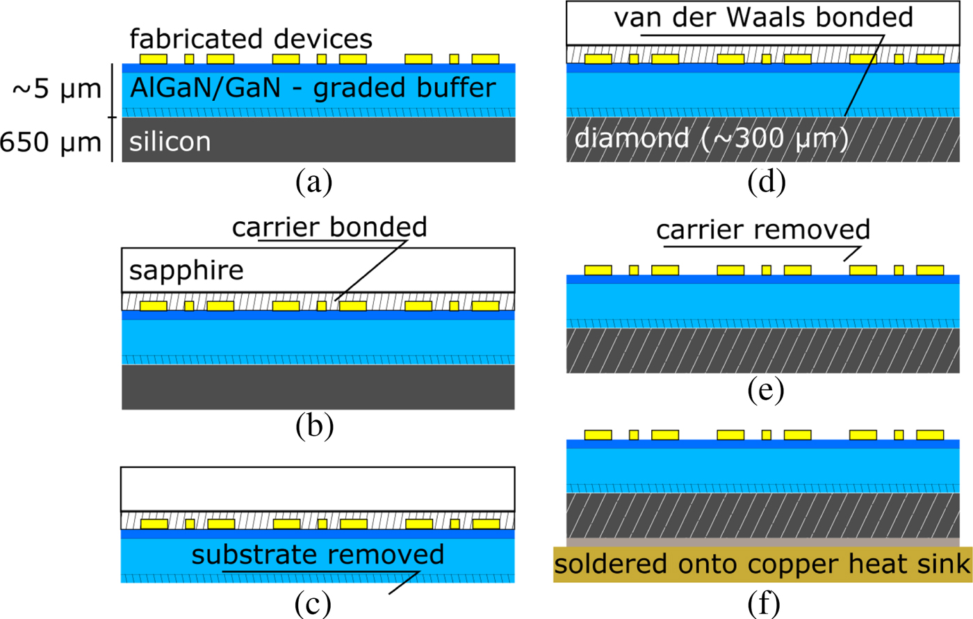
Fig. 2 shows a summary of the different process steps in GaN-on-diamond technology. After device fabrication on GaN-on-Si wafers and dicing into 12 mm × 12 mm reticles (2a), the device layer is transferred onto a sapphire carrier (2b). The Si substrate is wet-chemically removed (2c) by an acetic mixture of hydrofluoric acid (49 wt% HF) and nitric acid (69wt% HNO3), as described in [Reference Williams and Muller29–Reference Bauhuber, Mikrievskij and Lechner31]. This etching is very isotropic on Si and highly selective to the AlN nucleation layer. The AlN nucleation layer is bonded onto a polished PCD or SCD substrate (2d) by vdW bonding as described in [Reference Yablonovitch23]. After a solid bond is established, the sapphire carrier is removed (2e) at elevated temperatures of about 200°C. Finally, the GaN-on-diamond chip is soldered to a copper heat sink with gold/ indium adhesion layers (2f).
GaN-on-diamond fabrication steps. After device fabrication on GaN-on-Si wafers (a) the transfer starts with adhesive bonding of the device layer onto a carrier wafer (b). In (c) the Si substrate is etched and the resulting AlN nucleation layer bonded (d) onto a polished diamond substrate (PCD or SCD). The carrier is removed (e) and the GaN-diamond hybrid soldered onto a copper heat sink (f).
Electrical measurements on RF-transistors and DC-diodes
3 GHz, 50 V load-pull measurements
3 GHz (50 V bias) load-pull measurements of RF-transistors with 2 × 300µm gate-width and 500 nm gate-length have been compared on silicon and on bonded SCD heat spreaders.
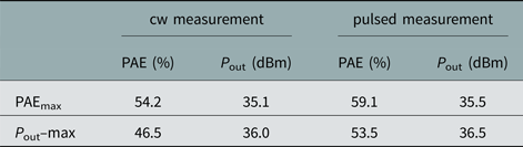
First, the output impedance was tuned to achieve maximum P out (P out–max) and PAE (PAEmax). Table 1 summarizes the best results achieved for GaN-on-Si transistors and its transferred GaN-on-SCD equivalent in continuous wave (cw) measurements. PAEmax improved from 50.6% (on Si) to 54.2% (on SCD) at similar P out of 5.65 W mm−1 and 5.39 W mm−1, respectively. P out–max was comparable on Si (6.79 W mm−1) and SCD (6.63 W mm−1), whereas PAE increased from 43.6% to 46.5%. However, the measurement of GaN-on-Si transistors on the wafer and GaN-on-SCD on isolated chips requires additional detailed characterizations to guarantee objective comparisons.
Maximum PAE and P out and corresponding P out and PAE for the 2 × 300µm gate-width transistor on SCD and Si

As summarized in Table 2 pulsed measurements on the GaN-on-SCD transistor revealed potentially much higher PAE and P out. In pulsed measurements, PAEmax increased from 54.2% to 59.1% at P out of 5.39 W mm−1 and 5.91 W mm−1, whereas P out–max increased from 6.63 W mm−1 to 7.44 W mm−1 at PAE of 46.5% and 53.5%, respectively.
Maximum PAE and P out and corresponding P out and PAE for the 2 × 300µm gate-width transistor on SCD - cw and pulsed
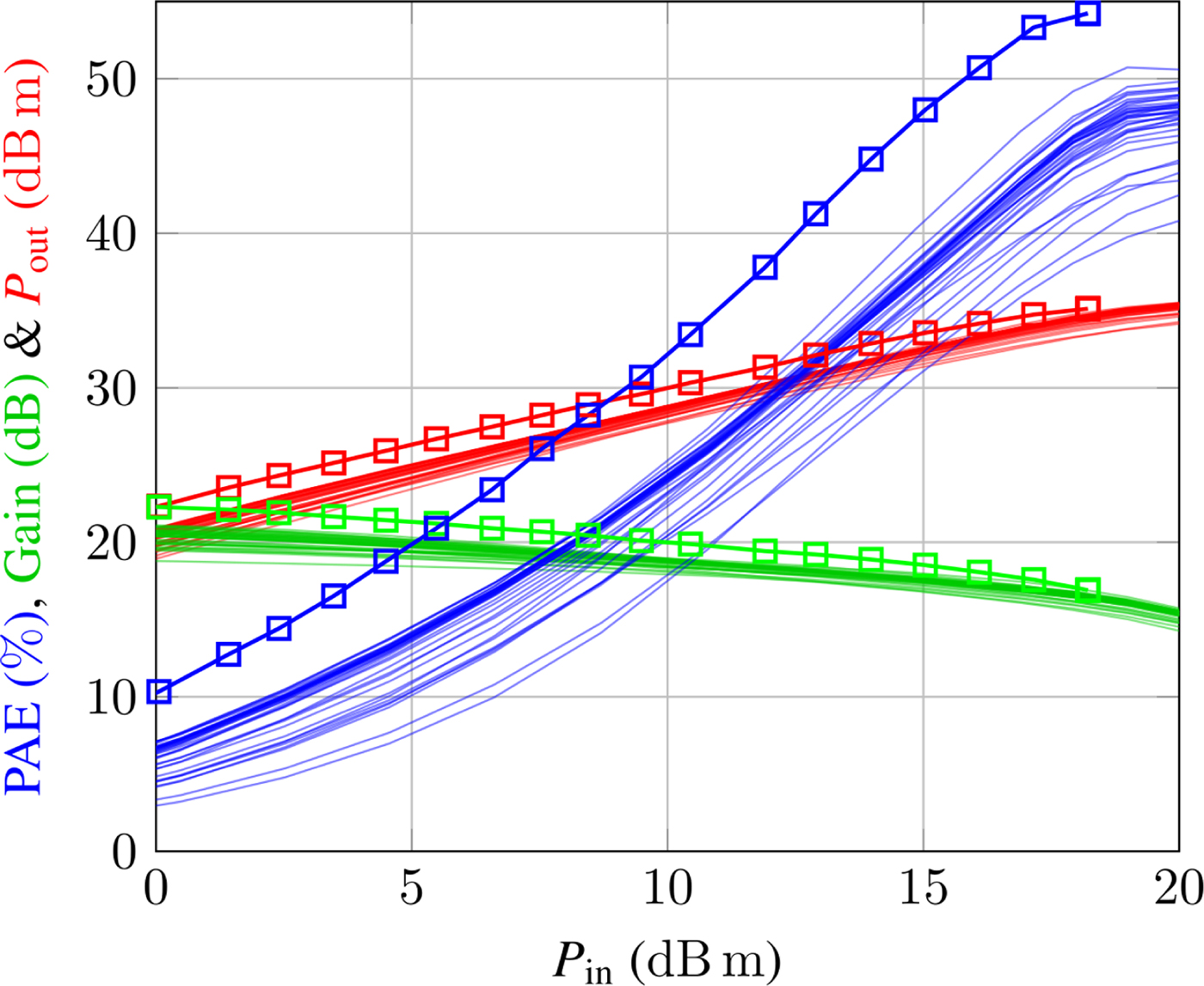
With output impedance fixed at maximum PAEs, load-pull measurements between a GaN-on-SCD transistor and the original GaN-on-Si transistors were compared. Fig. 3 shows PAE (blue), gain (green), and P out (red) for different input power levels (P in) on SCD (with symbols) and Si (no symbols). For P in < 15 dBm GaN-on-SCD achieved small improvements in PAE, gain and P out compared with all GaN-on-Si equivalent transistors. For P in > 15 dBm P out and gain curves approach the values of GaN-on-Si.
Load-pull measurement results of PAE (blue), gain (green) and P out (red) on RF-transistors with gate-widths of 2 × 300µm operated at 3 GHz, 50 V DC bias and constant load (load at maximum PAE). The transistor transferred onto SCD (with symbols) shows higher PAE than any GaN-on-Si transistor (other curves) at any input power level. At low input power, gain and P out is also higher on SCD but approximates the Si devices at higher input power.
The underlying complexity of the large sequence of critical fabrication steps to final GaN-on-SCD devices suggests that further improvements are quite probable. These first experiments successfully demonstrated that RF-transistors can be transferred from Si onto SCD without any observable performance degradation. Small improvements in PAE were recognized at comparable P out levels.
DC-Measurements on 2x1 mm2 diodes
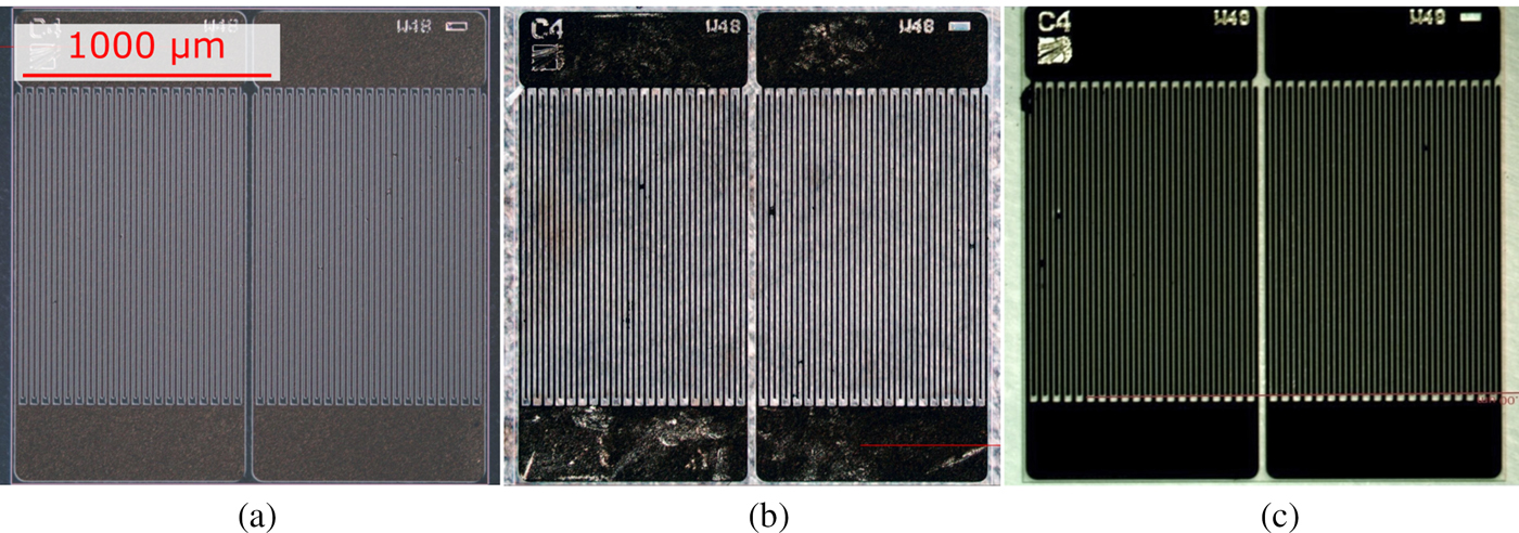
To characterize the GaN-on-diamond technology on larger devices, 2 mm × 1 mm AlGaN/GaN-diodes were transferred from Si onto PCD and SCD substrates. In Fig. 4 differential interference contrast (DIC) micrographs show the different appearance of two adjacent AlGaN/GaN-diodes on Si (Fig. 4a), PCD (Fig. 4b) and SCD (Fig. 4c). Si appears dark, whereas PCD and SCD diffusively scatter the light. PCD is easily distinguished by the visible grains in the background. The diodes (17µm channel length) have a channel width of 48 mm distributed over 40 fingers. The specific structure of this Schottky diode was reported in [Reference Weiss32].
Optical micrographs (DIC) of 2 mm × 1 mm diodes bonded onto Si (a), PCD, (b) and SCD (c). All diodes are fully operable without any cracks of the GaN device layer.
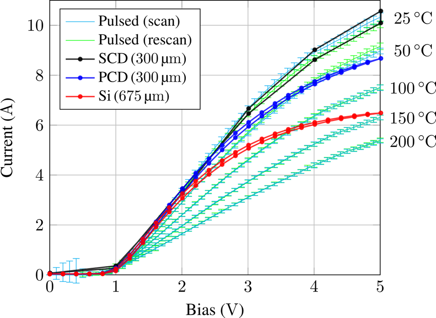
In Fig. 5 we increased the bias voltage (VBias) from 0 to 5 V on Si (red), PCD (blue) and SCD (black). Each bias point was kept for 10 s to apply a large heat load, whereas the baseplate temperature below the copper block regulated to constant 40°C. In our following electrical and thermal analysis, the 5 V power levels of 32, 43 and 52 W for Si, PCD, and SCD,respectively, are compared. For SCD an increase to 10 V results in a power of 130 W (not shown), which would probably destroy the diode on Si.
Currents in GaN-diodes on Si (red), PCD (blue), and SCD (black) and pulsed measurements (1 ms) on identical diodes of a similar wafer for increasing/ decreasing bias (cyan/green) and different baseplate temperatures (25°C–200°C). The standard deviation results from all diodes on the wafer.
Thermal analysis of diodes on SCD, PCD, and si
Temperatures from electrical analysis
In the section 3 electrical measurements, RF-transistors and diodes were shown. Whereas RF-transistors were only transfered onto SCD, our diodes were bonded onto both SCD and PCD. In contrast to our transfer of RF-transistors, the bonding process with diodes is well-engineered. The diodes are optically homogeneous bonded and demonstrate a large increase in diode currents on both SCD and PCD. The simplified structure of diodes compared with transistors facilitates our electrical and thermal analysis and allows the quantification of channel temperatures present in our diodes.
The slope of all diode curves (grown on Si and transferred onto SCD/PCD) in Fig. 5 is identical for small bias voltages where almost no heat is present. This slope ∂U/∂I is related to the on-state resistance
 $$R_{{\rm on}}=\partial U/\partial I = {l \over w}R_{ch}+R_C = {l \over w}{1 \over q\mu n_s}+R_C,$$
where l and w are length and width of the channel, respectively. R C includes contact resistances and R ch is the channel resistance between the contacts. R ch resolves to the inverse product of the elementary charge q, the electron mobility μ and the carrier density n s. The identical on-state resistance at low bias on all substrates shows that our transfer process does not change the AlGaN/GaN structure and that different currents at higher bias are predominantly caused by a temperature effect. The current saturation at higher bias is based on a channel pinch-off from the increasing channel potential [Reference Kuzmík33]. Saturation was observed on SCD around 10 V, whereas on silicon the channel saturates already at 5 V with currents of 13 and 6.5 A, respectively. Since electron density is almost constant with temperature [Reference Daumiller34], improved transport is mainly based on higher mobility.
The temperature dependence of electron mobility in AlGaN/GaN devices (> 300 K) is modeled with
 $$\mu _0=\mu _{300} \left({T \over 300}\right)^{-\alpha },$$
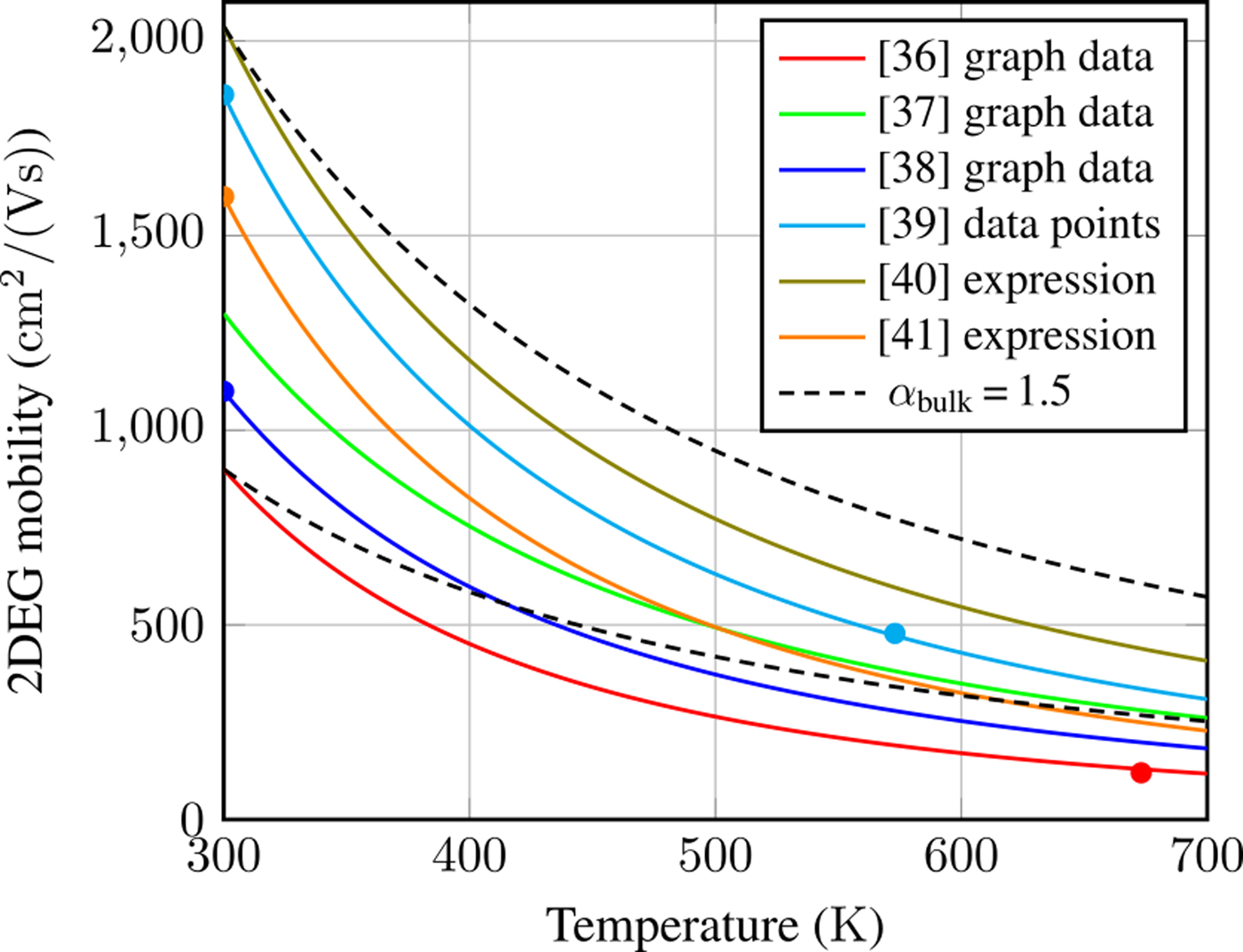
where μ 300 is the low-field mobility at 300 K and α a positive exponent. Generally, the bulk mobility in GaN is dominated by polar optical phonon scattering giving α bulk = 1.5. In the two-dimensional electron gas of AlGaN/GaN heterostructures, however, the exponent is higher and depends on the carrier density (see compiled data in Fig. 6). Moreover, at large electrical fields > 50 kVcm−1 [Reference Schwierz35], the mobility-field dependence cannot be neglected. However, the average field in our diodes with l = 17µm at 5 V bias results in electric fields < 3 kVcm−1, thus, mobility can be assumed to be independent of the electrical field. AlGaN/GaN transistors have highly inhomogeneous electric fields along the channel, which complicates the analysis of the temperature dependent mobility. In contrast, the employed lateral Schottky diodes with only two contacts exhibit an almost constant electric field. Therefore, changes in the current can be assigned directly to the temperature dependence of the mobility, i.e. larger currents result primarily from lower channel temperatures.
Experimentally determined AlGaN/GaN Hall mobilities from different groups [Reference Maeda36–Reference Lee41]. If distinct measurement points (marked as ‘data points’) or analytical expressions (‘expression') were not mentioned, equation (4.2) together with points read from plotted graphs were used (“graph data”). At 430 K (157°C) mobilities are 61%–83% larger than at 330 K (57°C). As comparison, the bulk mobility (black, dashed) decreases by only 45%.
The channel temperatures were quantified by comparison of pulsed (1 ms) measurements on identical Schottky diodes on a silicon substrate (on-wafer) with the I–V characteristics of the diodes on SCD, PCD, and Si (Fig. 5). Within the employed measurement system for these high-voltage diodes, charging effects require comparably long pulse lengths to prevent any electrical measurement errors. The thermal error due to electrical self-heating was corrected through our subsequent thermal simulation.
For pulsed measurements the baseplate and approximately the whole wafer was kept at constant temperatures (25°C–200°C) and it is assumed that the short load generates no significant heat. At low bias, the 25°C curves perfectly overlap with all measured diodes (SCD, PCD, and Si). At larger bias, the currents on PCD and Si reduce due to decreased mobility. In contrast, the diode on SCD follows the 25°C line, thus the generated heat is efficiently removed from the channel. It should be noted, however, that the limited pulse length generates some heat in the channel adding some temperature error. In first approximation this 1 ms pulse error adds some defined temperature offset depending on the bias, but not on the baseplate temperature. The relative error in this analysis therefore shrinks with higher baseplate temperatures. The measurements of our diodes on SCD, PCD, and Si were performed at baseplate temperatures of 40°C, it is therefore reasonable to assume that the channel temperature in our 25°C pulsed curve at 5 V bias equals at least 40°C. The 5 V bias temperatures on PCD and Si are 50°C and 150°C, respectively. To verify these assumptions, the temperature dependence of the mobility in Fig. 6 was taken into account. As shown above, the saturation current on SCD is 100% higher in comparison with the diode on a silicon substrate. The corresponding 100% change of the mobility can easily be explained by a change of the temperature 423 K (channel temperature on silicon as extracted from Fig. 5) to about 315 K, i.e. about 42°C in agreement with the similar discussion above. If the channel temperature on SCD would be significantly higher, Fig. 6 would give unrealistic high channel temperatures on silicon substrates. The extracted channel temperature is the base for the following thermal simulations.
3D thermal simulation
3D FEA (COMSOL) simulates the channel temperatures generated by electrical Joule heat in the diode's channel region. In literature, thermal simulations are widely employed and experimentally verified by Raman thermography [Reference Beechem42,Reference Kuball and Pomeroy43] and thermoreflectance [Reference Cho44–Reference Martin-Horcajo46]. As in our electrical analysis, the simpler structure of our large diodes compared with complex RF-transistors allows an accurate analysis based on relatively few assumptions. By changing the TBR between the GaN buffer and the substrate, temperatures extracted from our electrical analysis are reproduced and the required TBRs estimated.
The thermal resistance within the buffer/substrate region is affected by several layers. The accurate thermal modeling of each layer is complex since material quality is gradually improving in growth direction. The close distance between channel and substrate as well as material specific interfacial resistances complicate the analysis and common diffraction limited optical measurement techniques cannot resolve the several nm thin interlayers. It is, therefore, accepted to introduce a transition layer with an effective TBR, which accounts for all nonidealities at the buffer/substrate interface [Reference Kuzmík47]. In GaN-on-Si devices such transition layer adds an effective TBR of 10 m2 K/GW [Reference Won22] which we introduced as 100 nm thin TBR layer of κ thermal = 10 W m−1 K−1 (COMSOL ‘thin-film’ boundary condition).
Symmetries were used to reduce the device geometry to one quarter of our multi-finger diode, which consisted of a 22 nm AlGaN cap layer, 4.5µm GaN buffer and the substrate (675µm silicon or 300µm PCD/SCD) soldered onto a large copper block. The copper block base temperature was set to constant 40°C in accordance with our electrical measurements. The measured electrical power at 5 V bias (cp. Fig. 5) was converted to heat flux applied to the AlGaN/GaN channel region. A heat load of 65, 53, 40 W/mm2 was allocated to the 17µm long and 1.2 mm wide channel region for SCD, PCD, and Si, respectively. The thermal conductivity of the 100 nm thin transition layer was varied between 10Wm−1K−1 and 0.2 Wm−1K−1 to reproduce the channel temperatures from our electrical analysis on devices with different substrates.
Fig. 7 shows the temperature distribution of 20 diode fingers on SCD (7a), PCD (7b), and Si (7c, d) with respective heat load at 5 V bias. Fig. 7c shows a hypothetical diode on 100µm thin Si to compare a thermally optimized Si chip against SCD (heat-flux therefore adapted from SCD). On 675µm Si our assumptions reveal channel temperatures of 160°C, which fairly matches the 150°C as deduced from our pulsed current measurements. As discussed, the minimum channel temperature of our diodes on SCD and PCD must be larger than the 40°C baseplate temperature. Also, we expect TBRs larger than on Si since all defect rich boundary layers are transferred with the devices onto our diamond substrates and the vdW bond is expected to add some additional thermal resistance compared with the grown interface on Si. For SCD, even the optimum TBR conductivity of 10 W m−1 K−1 (equals TBRSi) still results in temperatures of 52°C, which is slightly higher than the ~ 40°C expected from our electrical analysis. We therefore assume that the transfer onto SCD does not add any significant thermal resistance compared with the already present GaN transition layer resistance.
3D thermal simulations (COMSOL) visualize temperature distributions in our 2 mm × 1 mm diodes - shown is only the channel cross section for clarity. (a), (b), and (d) show our electrically measured structures with adapted κ TBR to account for measured current differences on SCD (a), PCD (b), and Si (d). (c) is a hypothetical 100µm thin Si substrate with heat load from SCD (a). The direct comparison shows that even thinned Si is easily outperformed by SCD.
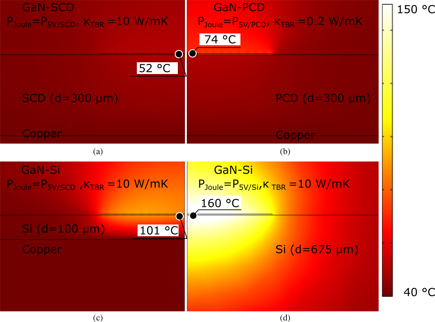
The difference between the SCD temperature extracted from electrical measurements and the thermal simulation suggests a similar offset for the PCD temperature. For SCD the simulated temperature was ~ 25°C higher, which is explained by the neglected limited current pulse. We, therefore, assume that the actual temperature on PCD should be also 25°C higher, i.e. 75°C. In our thermal simulation a temperature of 74°C is simulated for a low thermal conductivity of 0.2 W m−1 K−1 for the transition layer, which is 50x larger than for SCD and Si (both 10 W m−1 K−1). The large TBR on PCD is explained from the thermally poor diamond nucleation layer. A hypothetical 100µm thick Si substrate (Fig. 7c) as compared with SCD shows a temperature difference of ~ 50°C, which clearly demonstrates the outstanding performance of our GaN devices on SCD (cp. Tab. 3).
Thermal FEA parameter values of joule heat (P5V), TBR and channel temperature (TCh) for AlGaN/GaN Schottky diodes on SCD, PCD, and Si. Bold values were calculated through FEA. For SCD and Si, a TBR of 10 m2 K/GW [Reference Won22] was assumed. The TBR of PCD is estimated from the temperature difference to SCD in our pulsed electrical measurements

A 100 nm TBR layer of κ thermal = 10 W m−1 K−1 equals an interfacial TBR of 10 m2K/GW (TBR = 100nm/κ thermal [Reference Kuzmík47]), which is in range of commonly measured TBRs on Si and SiC [Reference Cho48]. The scatter in compiled values, and the uncertainty in individual measurements is considerably high. For GaN-on-diamond fabricated by Element Six, TBRs of 18m2K/GW–27 m2K/GW at 50 nm to 324 nm thickness are reported [Reference Won22], which match the TBR of Si. In their process, the negative impact of the diamond nucleation layer might by compensated by the removal of low-quality GaN nucleation layers before diamond growth, whereas our process still includes these thermally poor GaN buffer layers. In contrast, our transfer process on SCD substrates does not impose an additional diamond nucleation layer but high-quality diamond directly at the buffer/substrate interface.
Summary
Our low-temperature GaN-on-diamond transfer process with its seamless integration into GaN-on-Si device fabrication offers significant advantages in flexibility over diamond growth techniques on GaN. Pulsed load-pull measurements achieved 7.43 W mm−1 P out with 53.5% PAE (3 GHz, 50 V bias) in these first results.
We quantified the cooling performance of hybrids fabricated by our transfer technique with simpler, large diode structures. The electrical analysis based on temperature dependent mobility data (cp. Fig. 6) and pulsed (1 ms) measurements (cp. Fig. 5) consistently predict channel temperature differences of > 100 K and an absolute temperature of ~ 150°C on Si at 5 V bias. 3D thermal simulations with an effective TBRSi of 10 m2 K/GW [Reference Cho48] result in a similar channel temperature of 160°C. The larger temperature in our thermal simulation is explained from the relative difference between the pulsed heat load in the channel and the measured substrate temperature. Based on this thermal model, SCD and PCD were introduced as alternative substrates and the TBR adjusted to reproduce the electrically predicted temperatures. For SCD, even a perfect TBR (= TBRSi of 10 m2 K/GW) reveals temperatures larger than the predicted ~ 40°C (minimum temperature set by baseplate temperature), which suggests that the thermal performance of SCD is excellently exploited and the vdW bonding adds no significant thermal resistance to our devices. On PCD, in contrast, the present diamond nucleation layer increases the TBR consequently reducing the currents, which demonstrates the benefits in SCD compared to PCD as high-power GaN substrates.
Our temperature measurements are based on several consistent assumptions, however, more detailed quantification is needed to remove uncertainties regarding the SCD and PCD thermal performance. Future work will focus on the transfer of RF-devices and quantify channel and interface temperatures by Raman thermography or thermoreflectance to allow a direct measurement of lattice and surface temperatures and compare our devices with state-of-the-art technology.
Acknowledgments
The authors acknowledge the continuing support of the Federal Ministry of Defense (BMVg) and the Bundeswehr Technical Center for Information Technology and Electronics (WTD 81).
 Thomas Gerrer received the M.Sc. degree in Microsystems Engineering from the University of Freiburg, Freiburg, Germany, in 2014 with a Master's thesis on Superresolution structured illumination microscopy. Since 2014 he has been working toward the Ph.D. degree at the Fraunhofer Institute for Applied Solid State Physics (IAF), Freiburg, Germany, on the development of GaN-on-Diamond HEMTs.
 Volker Cimalla received his M.Sc. in 1993 and his Ph.D. in 1998 in Engineering from the Ilmenau University of Technology. In 1999–2001, he worked at the Foundation of Research and Technology Hellas (FORTH), Heraklion, Greece on the growth optimization of wide band gap semiconductors (SiC, GaN, metal oxides). In 2002–2007, he was research assistant at the Ilmenau University of Technology working on wide band gap semiconductors for chemical sensors and MEMS. In 2008, he joined the Fraunhofer Institute of Applied Solid State Physics (IAF) as a leader of the Microsensors group. Currently, he is the Head of the Department of Emerging Materials at Fraunhofer IAF.
 Patrick Waltereit received a Ph.D. degree in Physics from the Humboldt-University Berlin in 2001 on growth and characterization of non-polar oriented GaN/AlGaN heterostructures. He worked as a post-doctoral researcher at the University of California in Santa Barbara, USA, from 2001 until 2004 investigating MBE growth for GaN-based electronic and optoelectronic devices. Since 2004 he is with the Fraunhofer IAF in Freiburg, Germany, working on GaN-based high-voltage and high-frequency devices. Currently he is a group leader in the III-V Technology Department and Deputy Head of the Power Electronics business unit.
 Stefan Müller received his diploma degree in Physics at the Justus-Liebig-University in Giessen, Germany in 1994. Since 1994, he has been with the Fraunhofer Institute for Applied Solid-State Physics, Freiburg, Germany working on atomic force microscopy and reliability of optoelectronic compound semiconductor devices. In 1999, he joined the Metal-organic Vapor Phase Epitaxy (MOVPE) group at the IAF and is responsible for the growth of GaN-based electronic and optoelectronic structures on silicon, sapphire, and SiC.
 Thomas Maier received his Dipl.-Ing.(FH) in communications engineering from the University of Applied Science, Offenburg, Germany in 1988. From 1988 to 2008 he was working in production and development of point-to-point radio systems and base station transceivers. Since 2008 he has been working for the Fraunhfer IAF, Freiburg, Germany. His main activities there are characterization of GaN devices, especially loadpull and test automation.
 Heiko Czap received his Diploma as Graduate Engineer (FH) in 2004 from the University of Applied Sciences, Offenburg. From 2004 to 2010 he works on Hardware and Software development. In 2010, he joined the Fraunhofer Institute of Applied Solid State Physics (IAF) working on reliability and failure analysis of microelectronic compound semiconductor devices.
 Oliver Ambacher obtained his diploma and his Ph.D. in Physics (both with honors) at the Ludwig Maximilian University and the Technical University Munich in 1989 and 1993, respectively. Subsequent to his habilitation in experimental physics in 2000 and his promotion to private lecturer in 2001, he was appointed full professor (C4) for Nanotechnology at the Technical University Ilmenau in 2002. Since October 2007 Oliver Ambacher is Professor for Microsystems Engineering/Compound Semiconductors at Albert Ludwig University Freiburg as well as the Director of the Fraunhofer Institute for Applied Solid State Physics (IAF). In 2017, he became the Professor for Power Electronics at Albert Ludwig University Freiburg.
 Rüdiger Quay received his diploma in Physics at Rheinisch-Westfälische Technische Hochschule (RWTH), Aachen, Germany in 1997 and a second diploma in Economics in 2003. He obtained his Ph.D. with honors in Technical Sciences at Technical University Wien, Vienna, Austria in 2001, and in 2009 he received the venia legendi (habilitation) in microelectronics, again at Technical University Wien. He currently is the Head of the business unit Power Electronics at the Fraunhofer Institute for Applied Solid State Physics (IAF), Freiburg, Germany. He authored and co-authored refereed 250 publications and four monographs.


