

Introduction
High-speed Internet access is nowadays available even in remote areas via high throughput Ka-band satellites [1,2]. The down- and uplink frequency bands are at 20 and 30 GHz, respectively. In mobile scenarios right- and left-handed circular polarization (RHCP and LHCP) is often used in combination with the four-color spot-beam scheme.
To point the pencil beam of a terminal antenna to a satellite, it has to be steerable. Compared with reflector antennas, arrays are known for their high beam scanning agility and their potentially low-profile designs. Due to the large frequency difference between the transmit (Tx) and the receive (Rx) bands often two separate antennas are utilized. However, an antenna that accommodates both bands in a single aperture could significantly reduce the overall size [Reference Jaschke3]. For operation in special applications or regions, these bands should be as wide as possible.
For an interleaved Rx/Tx array dual-band antenna elements are necessary. Patch antennas featuring either dual-polarization or dual-band operation have been presented in [Reference Luo4], while [Reference Rohrdantz5] proposes a combined solution. However, both are rather narrowband.
Lenses have been shown to be a powerful means of shaping an antenna's radiation pattern and input matching [Reference Filipovic, Gearhart and Rebeiz6–Reference Jaschke, Rohrdantz and Jacob9]. In this contribution, we propose as a potential array element a novel end-fire arrangement consisting of an substrate integrated waveguide (SIW) such as in [Reference Kuhlmann, Rezer and Jacob10] terminated by a dielectric lens (see Fig. 1). The lens is needed to optimize both the input matching and the radiation pattern over wide frequency bands [Reference Jaschke11].
Dual-polarized SIW lens antenna.
Dual-polarization is realized by means of an orthomode transducer (OMT) combining a septum polarizer with a taper. Septum polarizers are used to excite circular polarization in square waveguides [Reference Ming and Tsandoulas12,Reference Ihmels, Papziner and Arndt13]. The taper allows avoiding thick multilayers [Reference Kuhlmann, Rezer and Jacob10,Reference Jaschke14] and it eases the transition to standard printed circuit board (PCB) technology, which, in turn, provides enough real estate for active component integration.
An alternative is wideband array antennas that can handle multiple bands in a single aperture. Examples are crossed Vivaldi [Reference Trott15] and tightly coupled dipole antennas [Reference Holland, Schaubert and Vouvakis16,Reference Bolt17]. A single polarized SIW H-plane horn antenna with an arc lens in the substrate is proposed in [Reference Lopez-Garcia8]. Dual polarization can be realized on a planar PCB [Reference Holland, Schaubert and Vouvakis16], although the available real estate for active components is very limited. Other designs use crossed PCBs to realize dual polarization [Reference Trott15,Reference Bolt17], which results in complicated setups.
In the following, we extend the results presented in [Reference Jaschke, Mitto and Jacob18]. In particular, we discuss technological improvements and report more details on the design procedure. Finally, three different antenna types are realized and compared to determine the best design compromise.
The proposed antenna concept is introduced in the section “Concept”. This is followed by the design of the lens and the OMT in the section “Design” . Next, the multilayer stack is defined and the manufacturing steps are explained. In the section “Measurements” the measurements are compared with simulation results for the OMT and three variants of the proposed antenna.
Concept
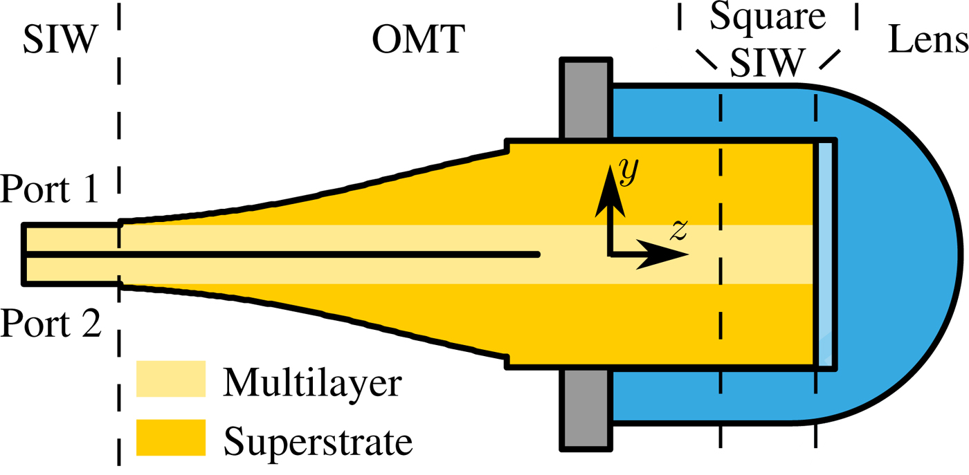
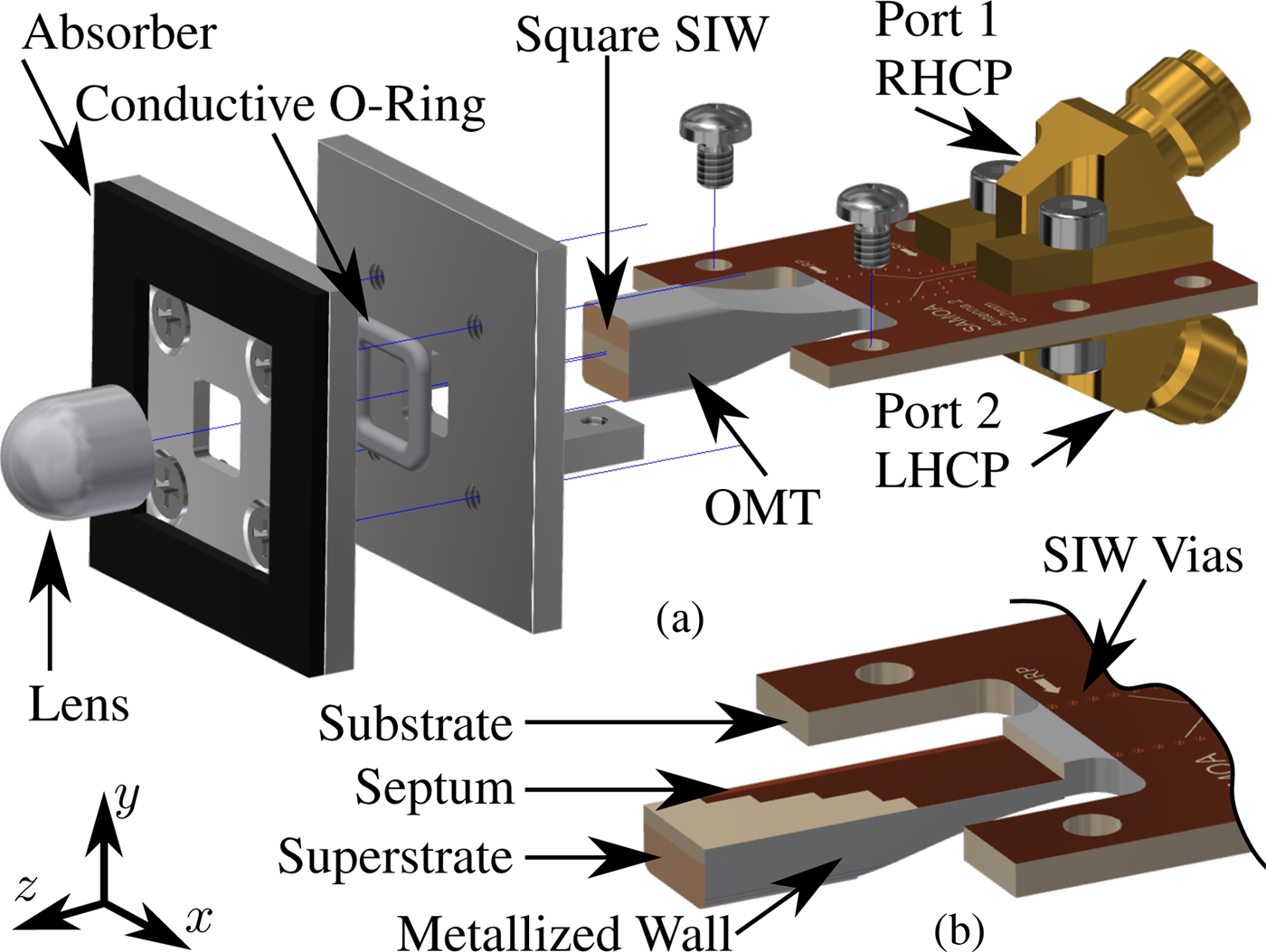
Figure 2 shows a cross-section (yz-plane) of the presented antenna element. The latter is composed of a hemispherical lens backed by a ground plane and fed by a square SIW. This SIW protrudes into a cavity on the backside of the lens. It supports two circularly polarized modes. These are formed in an OMT from the two linearly polarized TE 10-modes at Port 1 and 2, respectively. The OMT additionally matches the height of the multilayer SIWs at the input to that of the square SIW on the antenna side. This transition is realized by means of a tapered superstrate that sandwiches the multilayer.
Cross-section (yz-plane) of the SIW lens antenna.
Design
Lens design
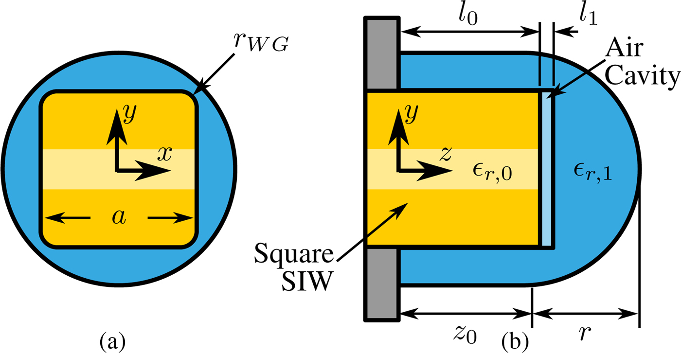
The end of the square SIW is covered by an extended hemispherical dielectric lens as depicted in more detail in Fig. 3. The lens has a radius r, a cylindrical extension of height z 0, and a square cavity of height l 0 + l 1 on the backside. The square SIW has a length l 0, a width of a = 4.7 mm, and rounded corners with radius r WG = 0.5 mm. The materials of the SIW and the lens are assumed to be homogeneous, non-dispersive, and with dielectric constants ε r,0 = 3.55 and ε r,1 = 2.1, respectively. This results in a cutoff frequency of 17 GHz for the degenerated fundamental modes of the SIW. An additional degree of freedom is given by the height l 1 of the air cavity (ε r = 1) between the SIW and the lens.
The lens profile is determined by a parameter study. The simulation is carried out with CST Microwave Studio. Because of the symmetry, only one of the (linear) polarizations is excited in the square SIW, here. Losses are neglected and an infinite ground plane is assumed as this saves simulation time. In addition, as the antenna is meant to be an element of an array finite ground effects are not of primordial importance, here.
Cross-section of the lens with square SIW feed in (a) the xy-plane and (b) the yz-plane.
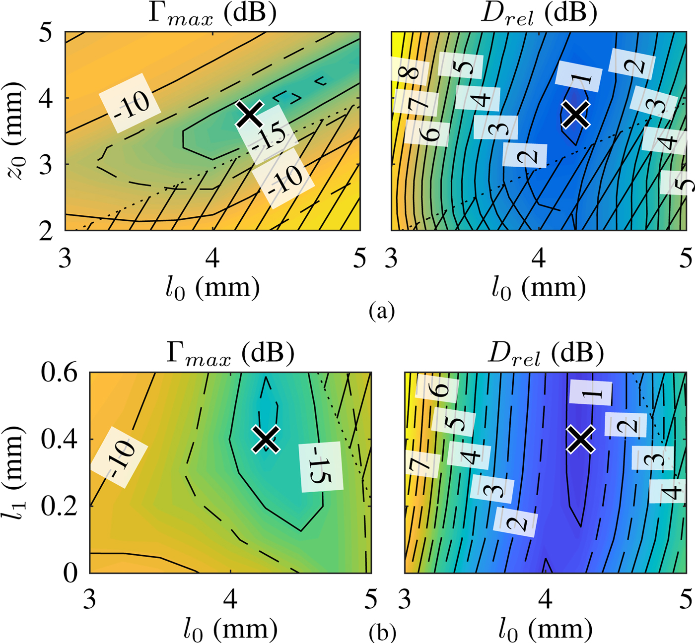
The lens radius is set to r = 3.5 mm and the parameters l 0 , l 1, and z 0 are varied. The performance of the antenna is assessed between 18 and 32 GHz by means of the maximal input reflection Γmax and the ratio D rel = D max/D min of maximal to minimal directivity in boresight direction. Small values of D rel thus relate to almost constant far-field patterns over frequency.
Contour plots for these parameters with l 1 = 0.4 mm are given in Fig. 4(a). Γmax is lowest when r + z 0 − l 0 is in the order of a quarter wavelength. For the parameter combination l 0 = 4.25 mm and z 0 = 3.75 mm an optimum is found and the directivity variation is low over the complete band. Figure 4(b) reports the influence of variations in l 0 and l 1 for constant z 0 = 3.75 mm. The gap l 1 has only little influence on D rel, which is optimal for l 0 = 4.25 mm. The parameter combination l 0 = 4.25 mm and l 1 = 0.4 mm yields a maximal input reflection of only Γmax = −18 dB and keeps the directivity variation at only D rel = 0.7 dB. Parameter combinations in the hatched areas are forbidden as the SIW arrangement is too long, there.
(a) Γmax and D rel versus l 0 and z 0 (l 1 = 0.4 mm). (b) Γmax and D rel versus l 0 and l 1 (z 0 = 3.75 mm).
This modified lens design improves the results from [Reference Jaschke11]. The lower frequency limit is decreased by 1.5 GHz by employing a larger waveguide with rounded corners and a slightly different lens shape whereupon the lens radius could be kept as small as before.
Orthomode transducer
Figure 5 shows the cross-section of the OMT in the yz-plane and in the xz-plane. The taper changes the height of each of the two input SIW from h 0 to h 1 = a/2 and the septum polarizer transforms the polarization from linear to circular. In the following, an even- and odd-mode analysis is applied to design the OMT.
Cross-section of the OMT in (a) the yz- and (b) the xz-plane (h 0 = 0.61 mm, l T = 8 mm).

For the even-mode, the xz-plane can be treated as a perfect electric conductor (PEC). The resulting structure is a rectangular waveguide taper with varying height h T(z). The characteristic impedance
 $$Z_C(z) = 2 \,Z_{TE}\displaystyle{{h_T(z)} \over a},$$
is given by the power-voltage definition and Z TE is the wave impedance of the fundamental TE-mode. For a given impedance profile Z C(z) the taper height h T(z) can be calculated. A Klopfenstein impedance profile yields an equal ripple input reflection [Reference Klopfenstein19]. Figure 6 depicts the ideal characteristic of a taper of length l T = 8 mm and with a 20 dB ripple above 18.8 GHz. The results of a full-wave simulation which takes into account the different dielectric constants and the rounded corners are shown for comparison. The agreement is very good, with the maximal input reflection being− 19 dB.
Input reflection (![]() ideal even,
ideal even, ![]() sim. even,
sim. even, ![]() sim. odd) and axial ratio of the OMT (
sim. odd) and axial ratio of the OMT (![]() sim.).
sim.).
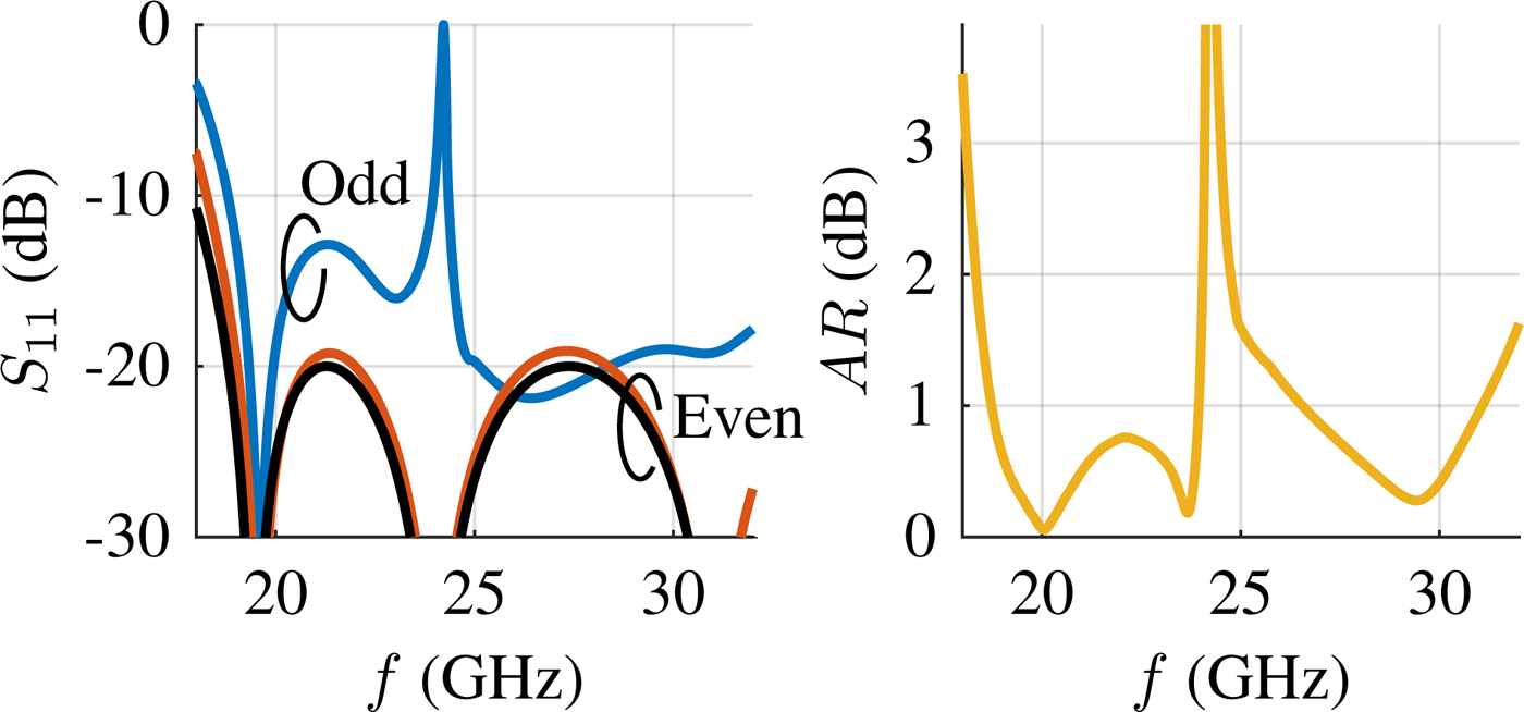
For the odd-mode, the xz-plane can be treated as a perfect magnetic conductor (PMC). The scattering parameters of the complete OMT are computed from the even- and odd-mode results. During the optimization process, the even-mode case is simulated only once, in contrast to the odd-mode model which is used to determine the septum geometry. Here, the widths w i, the lengths s i, and the position s 0 are systematically varied. The input reflection and the axial ratio are optimized in the frequency bands from 19 to 23 GHz and 27 to 31 GHz. The optimized parameters are listed in Table 1 and the results are plotted in Fig. 6. In the considered bands the input reflection of the odd-mode remains below − 13 dB and the axial ratio is smaller than 0.8 dB. The resonance at 24.3 GHz is due to the septum polarizer. This is a common effect which is known to limit the usable bandwidth of septum polarizers [Reference Esteban and Rebollar20]. In the particular dual-band application considered here, it can be tolerated, though, as it falls between the two sub-bands.
Parameters of the OMT

Antenna, lens, and OMT assembly
The next design step consists of combining the OMT and the lens antenna. In the lower band, only the two degenerate TE-modes are above cutoff and the input reflection of the OMT is only slightly altered by the well-matched lens. The length d between the OMT and the end of the square SIW has thus almost no influence. This changes in the upper band, where additionally the TM 11 and TE 11 modes can propagate as their cutoff frequencies are 24.3 and 24.9 GHz, respectively. The simulated coupling from the OMT input into these modes is only − 14 dB and − 27 dB, respectively. However, as these modes experience a substantial reflection of, respectively, − 2.5dB and − 5 dB at the lens, resonances may occur in the SIW section. These exhibit a moderate quality factor and, thus, could significantly degrade the transfer characteristic of the assembly. To precisely assess this effect, the OMT and the lens antenna are simulated taking losses into account and their scattering matrices are concatenated according to the model in Fig. 7(a). It turns out that, as a result of its weak excitation, the TE 11-mode can be neglected. It is thus not included in Fig. 7(a).
(a) Equivalent circuit of the antenna assembly. (b) Ratio H/V versus frequency and square SIW length d.
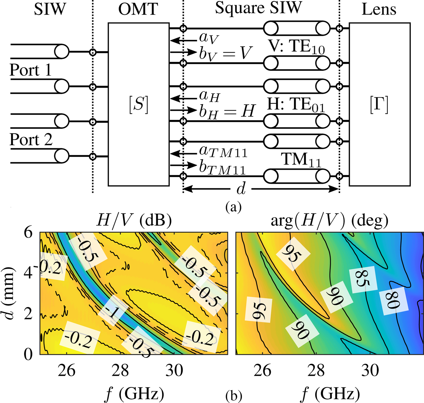
The axial ratio at boresight can be estimated from the transfer functions from one of the OMT inputs to the TE 01- and the TE 10-mode, respectively. In the following, these are labeled H (horizontal) and V (vertical), respectively. Circular polarization calls for equal magnitude and 90° phase difference. The axial ratio is better than 1 dB for − 0.5 dB ≤ H/V ≤ 0.5 dB and 85° ≤ arg(H/V) ≤ 95°. Figure 7(b) is a contour plot of H/V versus frequency and length d. The magnitude plot reveals areas, where resonances occur. Here, H/V is decreased by as much as 1.8 dB. In one of these areas as well as at low frequencies, the phase difference is larger than 95°. At higher frequencies, the difference drops below 85°.
For d = 0 mm the first SIW resonance occurs at 30.2 GHz, and thus, limits the usable band. For higher values of d the resonance frequency is decreased and thus the band above this resonance becomes usable. For d = 2 mm and d = 3 mm the first resonance occurs at 28 and 27.2 GHz, respectively. As the dependence on d is critical, it will also be investigated experimentally with d = 0 mm, d = 2 mm, and d = 3 mm. The resulting prototype antennas are labeled Ant. 1, Ant. 2, and Ant. 3 in the following.
Realization
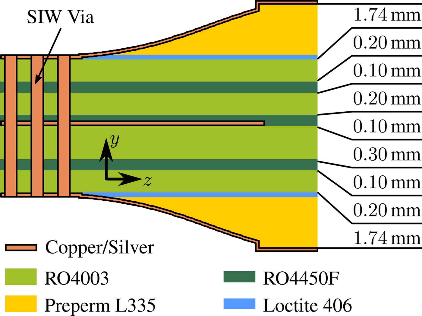
The antennas are realized based on a standard multilayer process with laminates from the Rogers RO4000 series. The layer stack is shown in Fig. 8 and the fabrication process is detailed in the following.
• In a first step, a multilayer with three copper layers is manufactured as depicted in Fig. 9(a). The middle layer separates the two SIWs and contains the septum from the OMT. On the outer layers SIW-to-CPW (coplanar waveguide) transitions [Reference Chen and Wu21] and footprints for the 2.92 mm-connectors (Rosenberger 02K80A-40ML5) are included.
• In a second step, the superstrates (Preperm L335) from Premix are glued on both sides of the multilayer with Loctite 406. The shape of the superstrates is dictated by the size of the square SIW and by the need to include holes for alignment pins as depicted in Fig. 9(b).
• In a third step, the taper of the OMT and the sidewalls of the square SIW are milled. The result is shown in Fig. 9(c).
• In a fourth step, the structures of the outer copper layers are covered by a kapton film (P-221) from Nitto as a matter of protection.
• Next, the complete structure is metallized. The process is offered by Jet Metal Technologies and is based on an innovative spraying technique.
• Finally, the kapton film is removed, unplated holes are drilled, and the antenna is milled out of the PCB as depicted in Fig. 9(d). As a result, the walls of the OMT and the square SIW are covered by metal, but of course not the antenna aperture.
Multilayer stack with superstrates.
Manufacturing steps of the SIW feed.
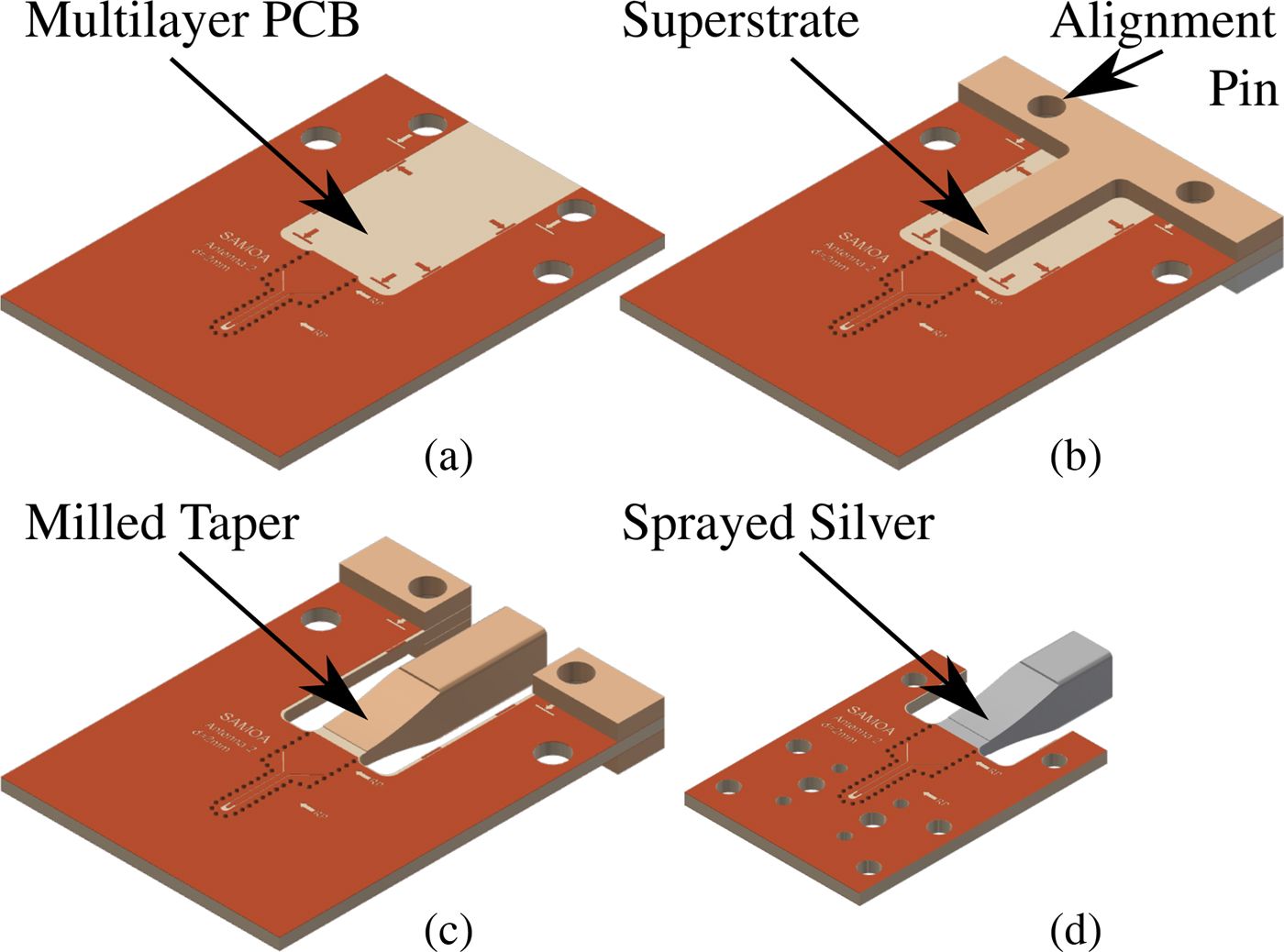
This manufacturing process represents a significant improvement compared with the manual one used in [Reference Jaschke, Mitto and Jacob18]. Multiple antennas can now be manufactured on a single PCB. For this, the manual metallization process, where conductive silver paint (L204N) from Ferro was used, is replaced by a batch process. In addition, this yields an improved conductivity, as will be shown below.
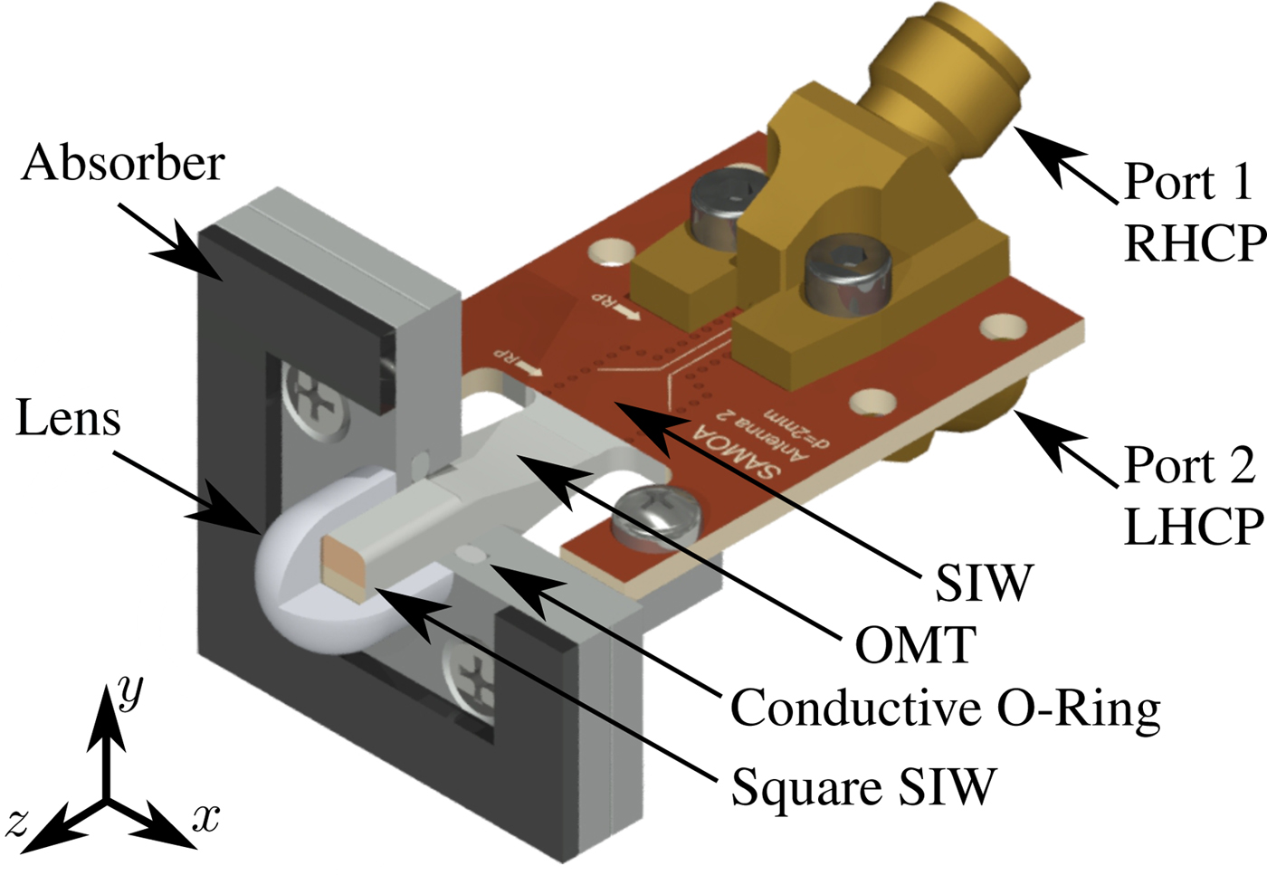
Figure 10(a) shows an exploded view of the complete antenna assembly. The lens and the ground plane are machined from PTFE and aluminum, respectively. Conductive O-rings from Soliani EMC in the ground plane ensure good galvanic contact to the square SIW. A 1 mm-thick absorber (Eccosorb BSR-U) with a 14 mm square cutout for the lens mitigates the effects of the finite ground plane. The absorber is glued on the ground plane (see. Fig. 10(a)). Figure 10(b) depicts the PCB. The square SIW is cut open to show the septum.
(a) Exploded view of SIW lens antenna and (b) cut view of the substrate with superstrates.
Measurements
Orthomode transducer
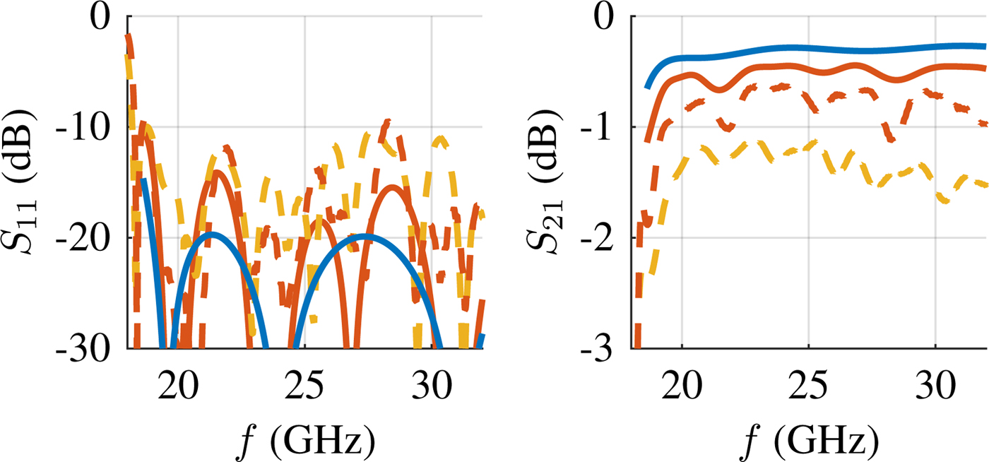
Figure 11 reports simulation and measurement results for the taper (even-mode). Measurements are carried out in a back-to-back configuration, where the taper and a mirrored taper are cascaded. The arrangement includes two 2.4 mm long sections of the multilayer and an 8 mm long section of the square SIW. In the measurements, the sprayed silver coating is compared with the conductive silver paint. Above 19.2 GHz the input reflection is below − 15 and − 10 dB in simulation and measurements, respectively. The measured insertion loss remains below 1.1 dB for the sprayed and 1.7 dB for the painted silver, respectively. On average, the sprayed silver reduces the insertion loss by 0.5 dB. The simulation predicts 0.2 dB lower losses for an effective conductivity of 1.5 · 107 S/m. In the simulation, a single taper has <0.4 dB insertion loss.
Scattering parameters of the taper (![]() sim.,
sim., ![]() meas.,
meas., ![]() single,
single, ![]() back-to-back with sprayed silver,
back-to-back with sprayed silver, ![]() back-to-back with silver paint).
back-to-back with silver paint).
Antenna, lens, and OMT assembly
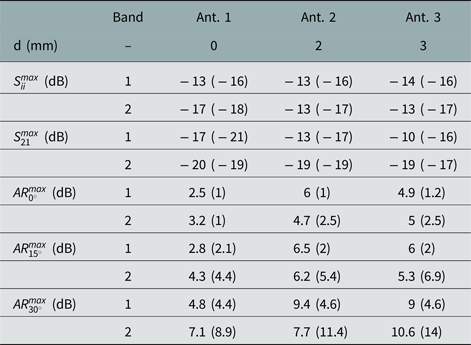
The scattering parameters at the two OMT input ports of the three antennas are depicted in Fig. 12. The reference planes are shifted to the multilayer SIW using a TRL calibration. The agreement between simulation and measurements is acceptable in most cases as discussed in the following. To assess and compare the performance of the antennas only the two relevant frequency ranges from 19 to 23 GHz and 27 to 31 GHz are considered. Here, all three prototype antennas exhibit a maximal input reflection of <-13 dB and <-16 dB in measurements and simulation, respectively. Only port 1 of Ant. 1 exhibits a higher reflection. This is due to the superstrate which did not correctly stick to the substrate at the taper input, leaving a gap. As this only marginally affected Port 2, the antenna performance could at least partly be assessed. While the measured (simulated) minimal port isolation decreases from 17 dB (21 dB) to 10 dB (16 dB) in the lower band, it remains almost constant at 19 dB in the upper one. The performance parameters of the three antennas are listed in Table 2.
Scattering parameters of (a) Ant. 1, (b) Ant. 2, and (c) Ant. 3 (![]() sim.,
sim., ![]() meas.,
meas., ![]() S 11,
S 11, ![]() S 22).
S 22).
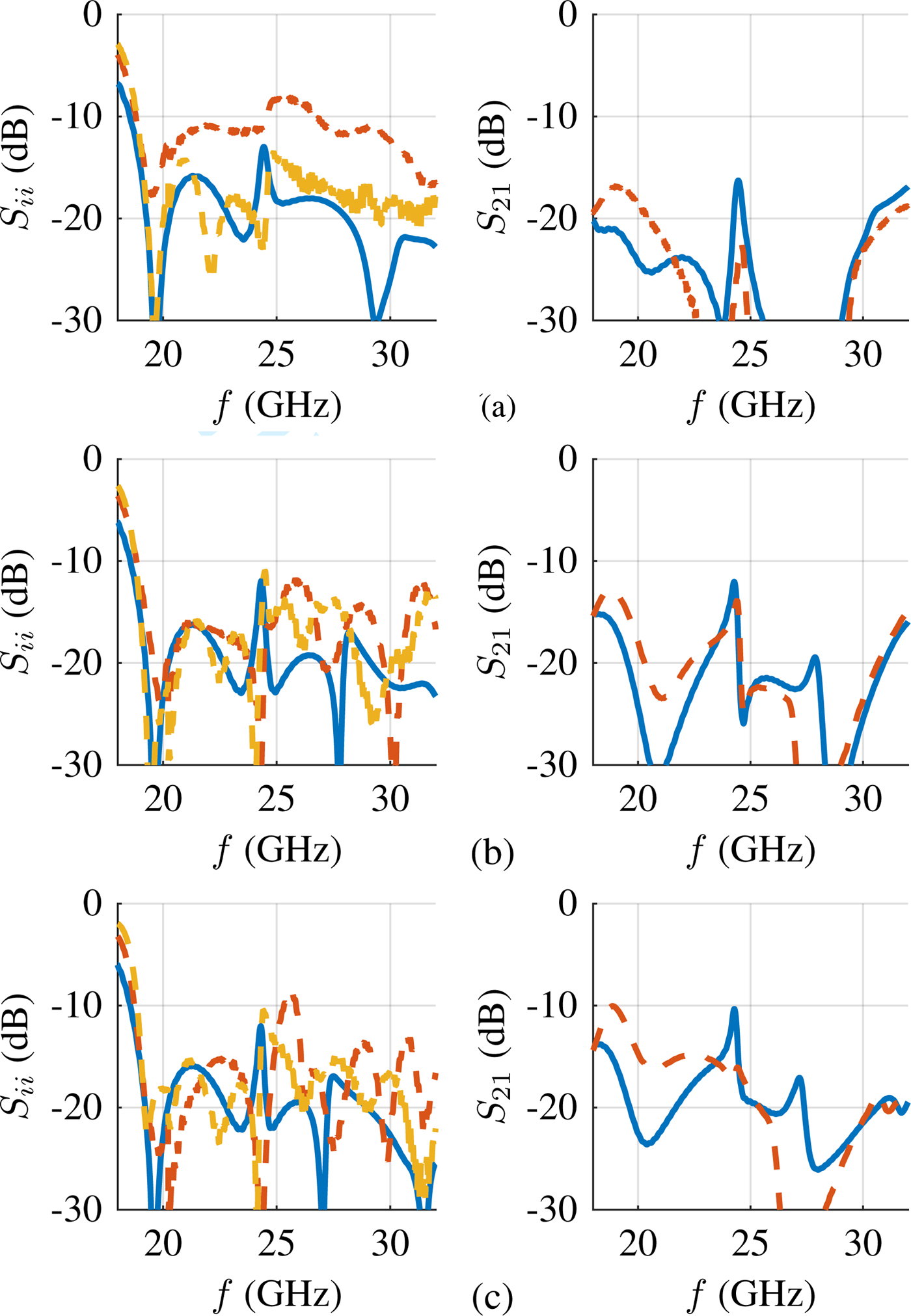
Measured (simulated) antenna performance parameters
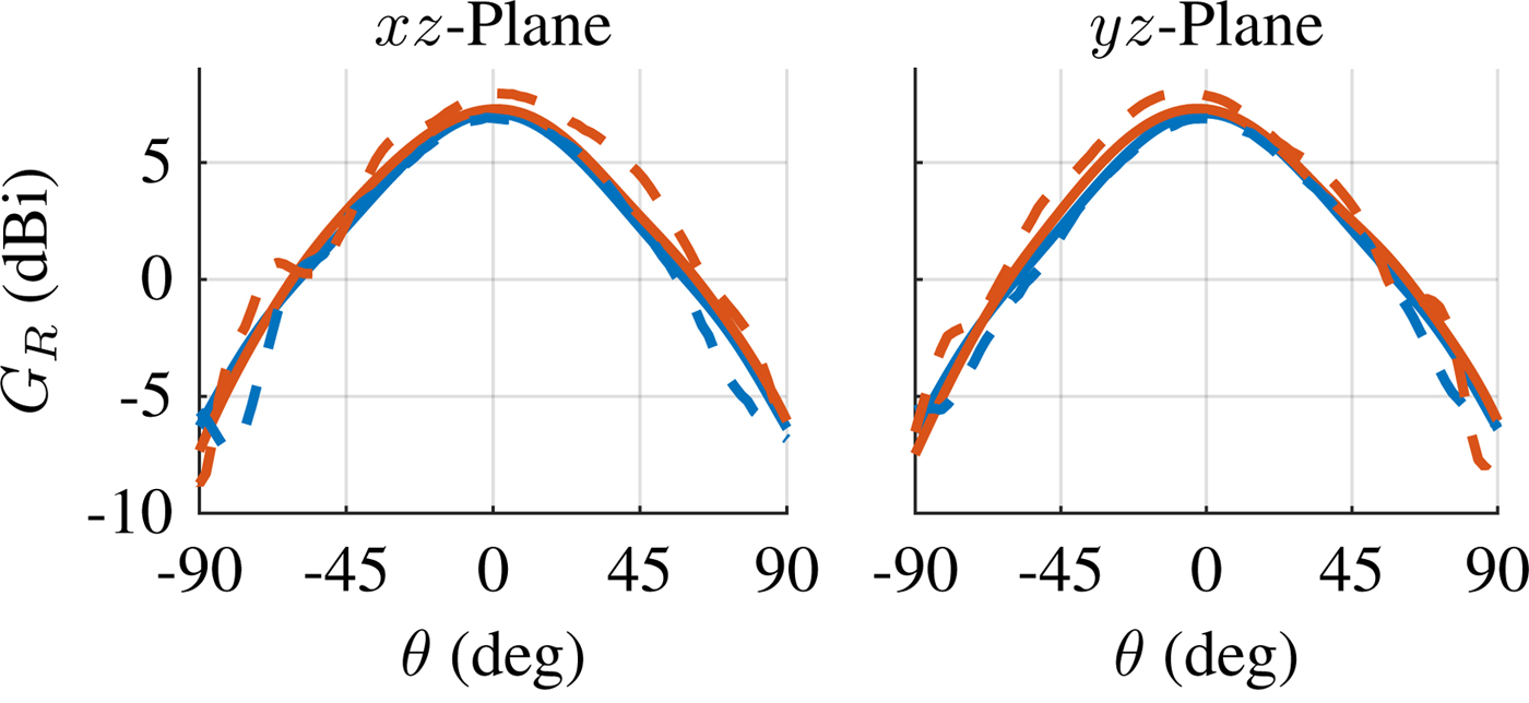
The antenna far-fields are measured in an anechoic chamber. The measurement data are power calibrated to the multilayer SIW and time-gated with a window of 3.5 m. In Fig. 13 the realized gain in the xz- and yz-plane is plotted versus the elevation angle at 20 and 30 GHz for port 2 of Ant. 1. It is consistent with the simulated results. The 3 dB-beamwidth is 66° and 72° at 20 and 30 GHz, respectively. The radiation patterns of the other antennas are very similar.
Realized gain in xz- and yz-plane for Ant. 1 (Port 2) (![]() sim.,
sim., ![]() meas.,
meas., ![]() 20 GHz,
20 GHz, ![]() 30 GHz).
30 GHz).
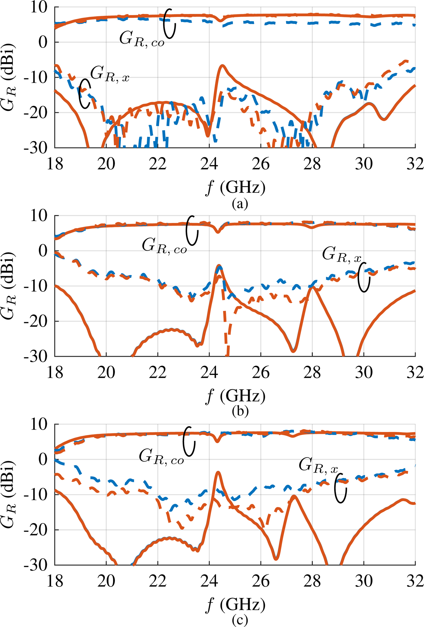
The realized gain in boresight direction for both RHCP (Port 1) and LHCP (Port 2) is plotted in Fig. 14. The co-polarized gain G R,co is very similar for all antennas. Except for the OMT resonance at 24.3 GHz, it ranges between 6.2dBi and 7.6dBi above 19 GHz in simulation. This is well confirmed by measurements. The gain of the defective Port 1 of Ant. 1 is up to 2.5 dB lower. Whereas the simulated cross-polarized gain G R,x of the different antennas is very similar in the lower band, it differs noticeably in the upper one. The SIW resonances of Ant. 2 and Ant. 3 are clearly visible at 28 GHz and 27.3 GHz, respectively, and confirm the findings in the section “Antenna, lens and OMT assembly”. Except for an increase towards lower and higher frequencies, the measured cross-polarized gain of Ant. 1 compares well with simulation, while Ant. 2 and Ant. 3 exhibit significant deviations.
Realized gain in boresight direction of (a) Ant. 1, (b) Ant. 2, and (c) Ant. 3 (![]() sim.,
sim., ![]() meas.,
meas., ![]() Port 1 / RHCP,
Port 1 / RHCP, ![]() Port 2 / LHCP).
Port 2 / LHCP).
The axial ratio AR is reported in Fig. 15. In the lower band, simulation yields values below 1.2 dB in boresight direction and below 2.1 and 4.6 dB in conical sectors of θ ≤ 15° and of θ ≤ 30°, respectively. In the upper band, the SIW resonances significantly impair the axial ratio. With values of 1, 4.4, and 8.9 dB for θ = 0°, θ ≤ 15°, and θ ≤ 30° Ant. 1 shows the best performance. The performances of Ant. 2 and Ant. 3 suffer from the fact that the resonances are within their operating band. These antennas are thus only useful in applications with shifted frequency ranges.
Maximal axial ratio in conical sector for Port 2 of (a) Ant. 1, (b) Ant. 2, and (c) Ant. 3 (![]() sim.,
sim., ![]() meas.,
meas., ![]() θ = 0°,
θ = 0°, ![]() θ ≤ 15°,
θ ≤ 15°, ![]() θ ≤ 30°).
θ ≤ 30°).
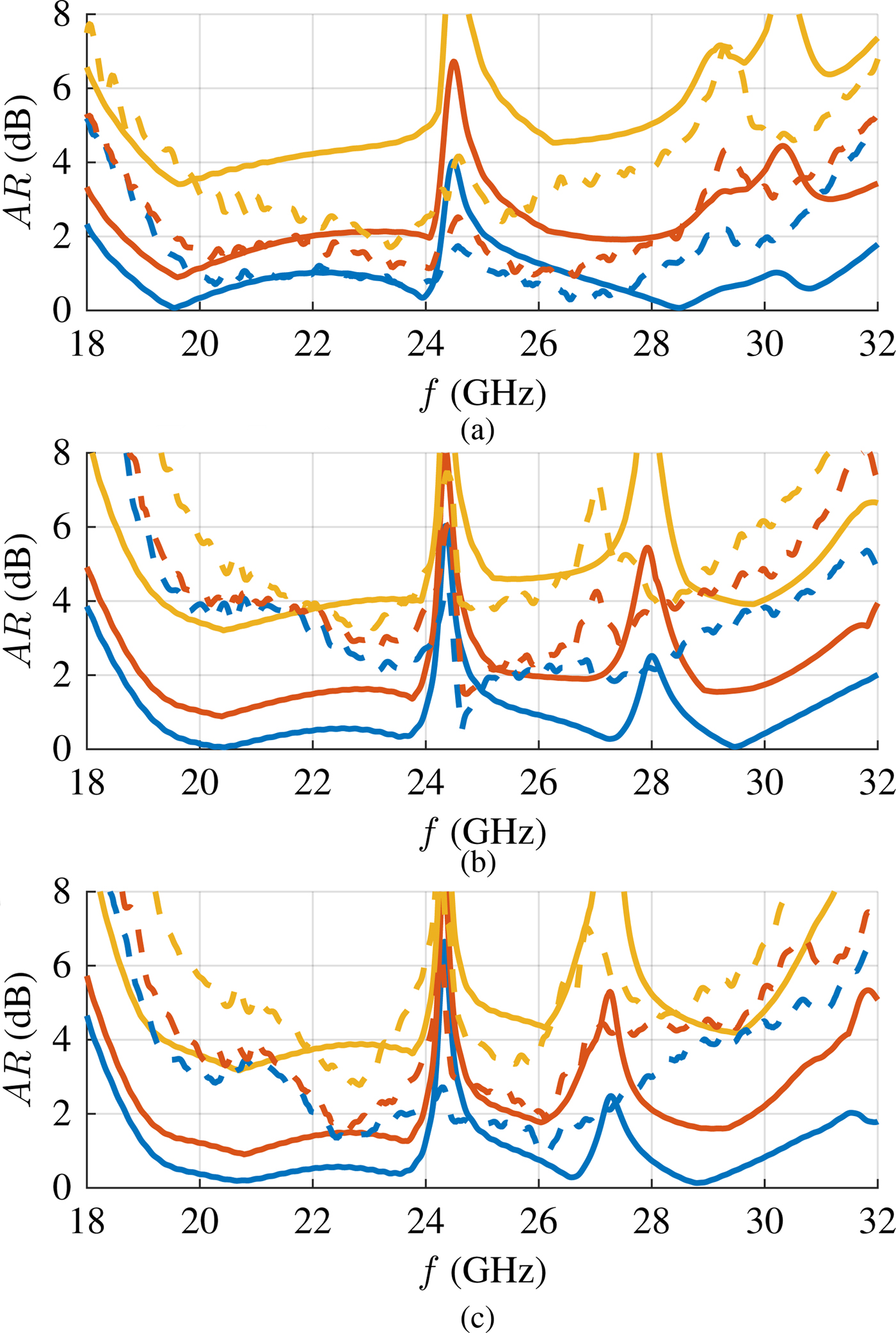
The measured axial ratio of Ant. 1 confirms the simulation in the middle of the operating band, but deteriorates towards low and high frequencies. The measured SIW resonance at 29.3 GHz is 1 GHz lower than simulated. As expected from the cross-polarization, the other two antennas show an even higher increase in the axial ratio. The performance data are summarized in Table 2.
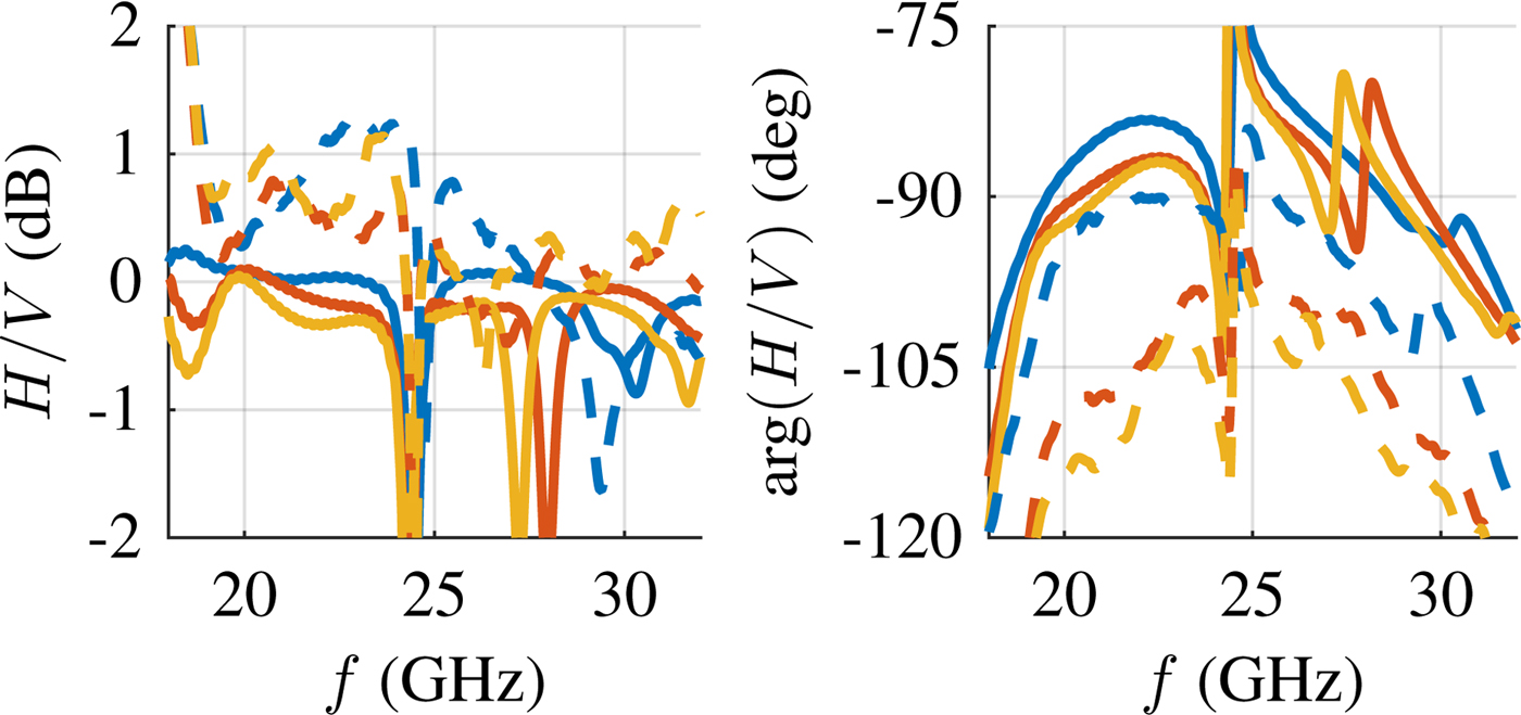
The ratio H/V in boresight direction plotted in Fig. 16 allows to further investigate the differences between simulation and measurements. In the simulation, significant dips are only visible at the resonances. In the measurements, the ratio varies from − 1.6 dB to 1.3 dB. However, the maximal axial ratio would be 1.6 dB, if H and V were in quadrature. For Ant. 1 the simulated phase error is only 5°. In the measurements, this error is increased to 18°, which is mainly caused by a steeper slope at low and high frequencies. For Ant. 2 and Ant. 3 the curves are shifted by approximately − 13° and − 18°. This is due to an increase of the propagation constant of the vertical TE 10-mode, which, in turn, is caused by the dielectric constant of the superstrate which is larger than assumed. This is confirmed by additional measurements in a split-cylinder resonator [Reference Janezic22] from which the dielectric constant of Preperm L335 is determined to be 3.6 instead of nominally 3.35. This also explains the lower frequencies of the SIW resonances. Of course, some uncertainty also results from inevitable manufacturing tolerances.
H/V for ![]() Ant. 1,
Ant. 1, ![]() Ant. 2, and
Ant. 2, and ![]() Ant. 3 excited at Port 2 (
Ant. 3 excited at Port 2 (![]() sim.,
sim., ![]() meas.).
meas.).
Conclusion
Dual-band SIW-fed lens antennas with dual-circular polarization for satellite communications at K/Ka-band are presented. The extended hemispherical lens is designed by means of a parameter study. A tapered OMT with septum polarizer generates circular polarization and connects SIWs of different heights. The SIW feed is manufactured in a standard multilayer PCB process with additionally bonded superstrates. These are shaped by milling. To reduce the conductive loss of the OMT and ease manufacturing, a batch metallization process is used. Finally, measurements of three antenna variants validate the concept. The measured axial ratio is higher than predicted by simulation, which can be explained by polarization-dependent propagation constants. The integrated Rx/Tx antenna with two independent circular polarizations exhibits the properties required in the intended application as an array element.
Acknowledgments
The authors wish to acknowledge funding and support by the German Aerospace Center (DLR) on behalf of the German Federal Ministry of Economics and Technology (BMWi) under research contract 50YB1707.
 Thomas Jaschke was born in Hamburg, Germany, in 1988. He received the B.Sc. and M.Sc. Degrees from the Hamburg University of Technology, Hamburg, Germany, in 2010 and 2012, respectively, where he is currently pursuing the Ph.D. degree with the Institute of High Frequency Technology. His current research interests include phased arrays, passive components, electromagnetic theory, and antenna measurements.
 Hans K. Mitto was born in Hamburg, Germany, in 1991. He received the B.Sc. degree in electrical engineering from the Hamburg University of Technology, Hamburg, Germany, in 2015, where he is currently pursuing the master's degree in microwave engineering, optics, and electromagnetic compatibility. His current research interests include passive filters in microwave circuits.
 Arne F. Jacob received the Dr.-Ing. degree from the Technische Universität Braunschweig, Braunschweig, Germany, in 1986.He was a Fellow with the European Organization for Nuclear Research, Geneva, Switzerland, from 1986 to 1988. In 1988, he joined the Lawrence Berkeley Laboratory, University of California at Berkeley, Berkeley, CA, USA, where he was a Staff Scientist with the Accelerator and Fusion Research Division for almost 3 years. In 1990, he became a Professor with the Institut für Hochfrequenztechnik, Technische Universität Braunschweig. Since 2004, he has been a Professor with the Technische Universität Hamburg–Harburg, Hamburg, Germany, where he heads the Institute of High Frequency Technology. His current research interests include the design, packaging, and application of integrated (sub-)systems up to millimeter frequencies, and the characterization of complex materials.


