


Introduction
Emerging communications applications such as 6G, Internet of Things and Internet of Space are increasingly calling for advanced radio frequency (RF) transceiver architectures able to support multiple communication standards and frequency bands [Reference Nguyen, Ding, Pathirana, Seneviratne, Li, Niyato, Dobre and Poor1, Reference Akyildiz and Kak2]. Furthermore, they will need to process a large amount of low-power RF signals in the presence of frequency-agile in-band and out-of-band interferers. As such high-performing RF hardware need to be incorporated in their RF front-ends to facilitate adaptive RF filtering alongside isolation. Impedance matching is also needed in these systems particularly in multi-antenna-phased array systems due to their loads deviating from 50 Ω during the beam scanning process.
Nonreciprocal components such as RF isolators or circulators are highly desirable in these systems as well as in emerging joint sensing and communication and V2V applications safeguarding high-power RF sources against undesired reflections or isolating two different parts of an RF transceiver. Conventional ferrite-based nonreciprocal components have been demonstrated to achieve a 10 dB isolation fractional bandwidth (FBW) ranging from 21% to 28.5%, with insertion loss (IL) values typically between 0.5 and 3 dB [Reference Sifat, Shams and Kishk3, Reference Marynowski4]. Additionally, research has explored tunable ferrite isolators with a tuning range spanning from 35 to 36 GHz, exhibiting an FBW of 8.4% and IL values between 2 and 3 dB [Reference Noferesti and Djerafi5]. Also, a tunable ferrite circulator centered at 3 GHz has been investigated with a tuning range of 1.3:1, FBW tuning range from 9.7% to 17.7% and IL between 2.7 and 4.5 dB [Reference Ashley and Psychogiou6]. While these components offer a relatively wide operating FBW and acceptable IL, they are bulky and expensive due to the need of external magnetic biasing. To overcome their size limitations and facilitate integration into integrated circuits (ICs), non-magnetic concepts using transistors are increasingly being investigated. However, they suffer from high-power consumption (2.6−40 mW) and high noise figure (NF) (3.2−14 dB) [Reference Chang, Kao, Lin and Wang7–Reference Nagulu and Krishnaswamy10]. In terms of RF filtering, multiple adaptive bandpass filtering (BPF) concepts have been investigated to date with wide tuning ranges as well as multiple levels of transfer function tunability [Reference Cho and Rebeiz11–Reference Anand and Liu13]. However, the majority of them are large in size or rely on low-quality-factor (Q) varactors that lead to large amounts of IL in their passband (around 1.9−7.6 dB) and are limited to frequencies as high as 1–2 GHz [Reference Cho and Rebeiz11, Reference Cho and Rebeiz12]. Tunable matching networks using RF switches, varactors, and micro-electromechanical systems (MEMS)have also been demonstrated [Reference Missen, Macheret, Semnani and Peroulis14–Reference Sánchez-Pérez, Andersson, Buisman, Kuylenstierna, Rorsman and Fager16]. However, they are large in size and lossy and they are rarely found in phased array systems.
To facilitate miniaturization in the RF front-end, codesign techniques or the realization of multifunctional RF components can be considered. In the domain of RF filters, codesign techniques are being increasingly explored to integrate them with couplers [Reference Liu, Li, Zhang, Fang and Wang17], amplifiers [Reference Gao, Shang, Li, Guo and Wang18], impedance matching networks [Reference Estrada, Johannes, Psychogiou and Popović19], isolators [Reference Ashley and Psychogiou20–Reference Dutta, Kumar and Ram29], circulators [Reference Ashley and Psychogiou22], and phase shifters [Reference Zhu, Yang, Chi and Xu30]. Notably, the integration of filters and isolators (i.e., BPFIs) primarily revolves around transistor-based configurations [Reference Ashley and Psychogiou20–Reference Ashley and Psychogiou22] and spatiotemporally modulated (STM) resonator arrays for example the ones discussed in [Reference Chaudhary and Jeong23–Reference Wu, Liu, Hickle, Peroulis, Gómez-Díaz and Álvarez Melcón28]. In transistor-based configurations, the unilateral properties of transistors are used to incorporate nonreciprocity. While these configurations exhibit gain (4.2−5.8 dB) and isolation (44–71 dB), their operating frequency remains static, and their power consumption is high [Reference Ashley and Psychogiou22]. STM resonator approaches use modulating passive resonators with phase-shifted low-frequency RF signals to achieve directional transfer functions. Although they can be made tunable, these concepts have only been demonstrated for frequencies between 0.14 and 1.46 GHz, with lower isolation levels of about 8−53 dB and IL between 1.5and 6 dB [Reference Chaudhary and Jeong23–Reference Zhang and Psychogiou25].
Considering the aforementioned RF front-end design and integration challenges, this paper introduces a new class of a tunable BPFI with the RF codesigned functionality of a tunable BPF, an RF isolator and a tunable impedance matching network, as shown in the block diagram and conceptual S-parameters in Fig. 1. The proposed concept is based on a new class of a tunable nonreciprocal frequency-selective stage (NFS), which demonstrates nonreciprocal frequency-selective power transmission in the forward signal propagation direction and signal cancellation in the reversed direction [Reference Li and Psychogiou31]. We demonstrate that by cascading various types of tunable stages, such as NFSs and tunable reciprocal resonators, different types of filtering and isolation transfer functions can be obtained. Frequency tunability and adaptive impedance matching can be realized in the BPFI by reconfiguring the NFSs which is shown in this work for the first time. Additionally, the paper offers a comprehensive design methodology considering various performance metrics such as stability, IL, directivity, NF, and third-order input intercept point (IIP3). The paper’s structure is as follows: The “Theoretical foundations” section outlines the operating principles of the proposed tunable NFS concept, its design trade-offs, impedance matching capabilities, and its application to codesigned tunable BPFIs. The “Experimental validation” section shows the experimental validation of the concept. Finally, the “Conclusion” section summarizes the main contributions of this work.
Tunable RF codesigned BPFI concept. (a) Block diagram. (b) Conceptual power transmission and isolation response. Black circles: tunable reciprocal resonators, grey circles with a triangle: tunable NFS, black lines: coupling elements.

Theoretical foundations
Tunable nonreciprocal frequency-selective stage
The circuit schematic and the S-parameter response of the NFS are illustrated in Fig. 2(a) and (b). It comprises two parallel branches: (i) a transistor-based branch, defined by a transistor and a resistive attenuating and matching network, and (ii) a frequency-dependent branch that also introduces a phase delay. The transistor’s unilateral properties result in distinct power transmission profiles in each direction of the NFS, namely the forward (from P1 to P2) and the reverse (from P2 to P1). Specifically, in the reverse direction of propagation, signal attenuation occurs at a frequency where the RF signals from the transistor-based path and the feedback reach P1 with a phase difference close to 180° and appropriate amplitude so that they cancel out, as depicted in the red trace in Fig. 2(b). Furthermore, in the forward direction, the RF signal from P1 reaches P2 after going through a loop formed by the feedback in series with the transistor-based path. When this loop has a zero-phase, the RF signals at P2 will be added in phase as shown in Fig. 2(b) − black line. It is also shown that as the operating frequency deviates from the center frequency, the balance of the RF signals through the two paths weakens, leading to a frequency-dependant power transmission response within the NFS.
(a) Circuit schematic of the tunable NFS based on coupled-line feedback. T: BFU760F, Vb = 0.78 V, Vc = 0.8 V, Cf1 = 1.14pF, Cf2 = 1.1 pF, R1 = 63.5 Ω, R2 = 18 Ω, R3 = 58 Ω, ZE = 163 Ω, ZO = 64 Ω, l = 36° at 1.7 GHz. (b) Circuit-simulated S-parameters of NFS at 1.7 GHz. (c) Circuit-simulated amplitude and phase response of S-parameters of transistor-based and coupled-line paths for the realization of the NFS at 1.7 GHz.

To better illustrate the operating principles of the tunable NFS concept, an NFS design is considered at 1.7 GHz using an NPN transistor (BFU760F) in a common emitter configuration. The transistor-based path is composed of a transistor and three resistors with the following characteristics: R1 = 63.5 Ω, R2 = 18 Ω, R3 = 58 Ω. As depicted in Fig. 2(c), the transistor path exhibits a positive phase of +84° at 1.7 GHz. Resistors R1, R2, and R3 are utilized for matching and stability. Furthermore, they are used to reduce the gain of the transistor path to 1.8 dB at 1.7 GHz, ensuring amplitude balance between the transistor path and the coupled-line feedback. Upon defining the parameters of the transistor path, a capacitively loaded coupled-line feedback is introduced in parallel. Its parameters are as follows: ZE = 163 Ω, ZO = 64 Ω, electric length l = 36° at 1.7 GHz, Cf1 = 1.14 pF, Cf2 = 1.1 pF, which realize the negative phase of −89° at 1.7 GHz. The capacitors in the feedback branch reduce the electric length of the coupled line, miniaturizing the NFS’s size. Consequently, at the NFS’s center frequency, the RF signals add constructively in the forward direction due to the zero-phase resonance in the loop composed by the transistor-based path and the coupled-line feedback. Furthermore, they cancel destructively in the reverse direction due to the approximate 180° phase difference between the two parallel paths. The power transmission and directivity at 1.7 GHz are 1.8 and 45 dB, respectively.
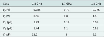
Center frequency tunability in the NFS can be incorporated by adjusting the capacitances of the capacitive loads that are added on the coupled line section through electronically reconfigurable varactors. Furthermore, the bias voltage of the transistor needs to be modified. This ensures that the amplitudes and phases between the two RF signal paths lead to constructive signal combination in the forward direction and destructive signal cancellation in the reverse direction at the desired frequencies of operation, as depicted in Fig. 3.
Circuit-simulated S-parameters of the reconfigurable NFS. Case 1.5 GHz: Vb = 0.785 V, Vc = 0.56 V, Cf1 = 1.49pF, Cf2 = 1.44 pF; Case 1.7 GHz: Vb = 0.78 V, Vc = 0.8 V, Cf1 = 1.14pF, Cf2 = 1.1 pF; Case 1.9 GHz: Vb = 0.775 V, Vc = 1.4 V, Cf1 = 0.85pF, Cf2 = 0.81 pF.

NFS design trade-offs
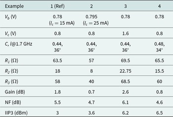
When designing the NFS, various trade-off performance characteristics between gain, directivity, impedance matching, stability, NF, and IIP3 must be carefully considered. Figure 4 illustrates two example NFS cases with different resistor values for R1. When a higher R1 is used (the rest of the circuit parameters are listed in Fig. 2), lower gain is obtained. However, the NFS remains unconditionally stable and achieves a directivity of approximately 45 dB. In contrast, reducing R1 to 50 Ω results in higher gain but conditional stability, poor impedance matching, and compromised directivity due to inadequate impedance matching and attenuation in the transistor-based path. Therefore, multiple parameters must be optimized in the NFS to ensure unconditional stability, good impedance matching, and high directivity.
Circuit-simulated (a) S-parameters and (b) stability factor of NFS when changing R1.

Table 1 presents four NFS design examples with their maximum directivity being greater than 40 dB, good impedance matching, and unconditional stability at 1.7 GHz, each with varying gain, NF, and IIP3. Their S-parameters are depicted in Fig. 5. Using Example 1 as a reference, variations in bias voltages of the transistor (Vb and Vc) and the coupling factor (C) of the coupled line are introduced in Examples 2−4, respectively, while optimizing R1, R2, and R3 to ensure high directivity, good impedance matching, and unconditional stability. Comparing the four examples, a trade-off between gain and NF is evident, whereby higher gain results in higher NF. IIP3 can be improved by increasing the transistor bias voltages, which also leads to increased power consumption. Alternatively, IIP3 can be enhanced by increasing C of the coupled line feedback. However, it should be noted that in a practical implementation scenario using transmission lines, larger Cs necessitate transmission lines with narrower widths or gaps between them, requiring higher manufacturing accuracy.
Circuit-simulated S-parameters of four NFS design examples in Table 1.

Four NFS design examples with optimal directivity, unconditional stability and impedance matching at both ports

Tunable RF codesigned bandpass filters and isolators
After determining the parameters of the NFS, tunable RF codesigned bandpass filters and isolators (BPFIs) can be implemented by cascading one or more NFSs and other tunable reciprocal resonators in series through impedance inverters, as depicted in Fig. 1. They can be designed using standardized coupled-resonator-based filter design techniques due to the resonant behavior of the NFS that allows it to be used in the filter design just as any other resonating node. Figure 6(a) illustrates a three-stage tunable BPFI comprising one NFS and two capacitively loaded half-wavelength long microstrip resonators implemented on a Rogers RO4003C with a thickness of 0.508 mm, dielectric permittivity of 3.55, and a dielectric loss tangent of 0.0027. In the BPFI, the NFS enhances the power transmission from P1 to P2 while it cancels the RF signals from P2 to P1 at the center frequency. The directivity of the BPFI matches that of the NFS. Additionally, when compared to a single NFS, the out-of-band isolation is higher due to the presence of reciprocal resonators. The tunable transfer function capabilities of the BPFI are shown in Fig. 6(b), which can be achieved by tuning the NFSs as discussed in the “Tunable nonreciprocal frequency-selective stage” section and by tuning the capacitively loaded microstrip resonators. The parameters for these tuning cases are listed in Table 2. The 3-dB BW of the three states in Fig. 6 are 0.17 GHz for the transfer function centered at 1.5 GHz, 0.2 GHz for the transfer function centered at 1.7 GHz, and 0.22 GHz for the transfer function centered at 1.9 GHz. To enhance the gain in the transmission direction and the isolation levels in the reverse direction, a higher number of NFSs can be incorporated into BPFI, as depicted in Fig. 7(a), in which two NFSs and one capacitively loaded half-wavelength long microstrip resonator are included. A comparison between the responses of the two BPFI topologies is provided in Fig. 7(b). As shown, gain and isolation are improved by using a higher number of NFSs, however at the expense of power consumption, noise and IIP3. In summary, the tunable BPFI can be scaled to higher-order transfer functions by adding more NFS units for increased gain and isolation levels. Also, reciprocal resonators can be added to enhance selectivity and out-of-band suppression.
(a) Block diagram of the three-stage BPFI (topology A) that comprises one NFS and two half-wavelength microstrip resonators. (b) Circuit-simulated tunable responses of (a). W01 = W34 = 0.685 mm, L01 = L34 = L12 = L23 = 26.6 mm, W12 = W23 = 0.6 mm, W1 = W3 = 8 mm, L1 = L3 = 39.5 mm.

(a) Block diagram of the three-stage BPFI (topology B) that comprises two NFSs and one half-wavelength microstrip resonator. W01 = W34 = 0.8 mm, L01 = L34 = L12 = L23 = 26.6 mm, W12 = W23 = 0.5 mm, W2 = 7.9 mm, L2 = 40 mm, C = 6 pF. (b) Comparison of the S-parameter response of topologies A and B.

Parameters for the tuning cases in Figure 6(b)

Tunable matching capabilities
The NFS can also be reconfigured to act as an adaptive matching network. This functionality is particularly relevant in phased array applications whose input impedance varies as a function of the beam angle. Figure 8(a) demonstrates the block diagram of the NFS when tuning Cf1 and setting its source (ZS) and load impedance (ZL) equal to 50 Ω which alters its input (Zin) and output (Zout) impedances as depicted in Fig. 8(b) and (c). Notably, Zin undergoes significant changes while Zout remains relatively stable, indicating the potential to achieve conjugate matching for varied ZS while Zout remains unchanged allowing to preserve the performance of the RF components that follow the BPFI in the RF front-end chain. Following the examination of the influence of Cf1 in NFS, further analysis is conducted on the impact of varying ZS on Zout while Cf1 is set to 1.14 pF, as shown in Fig. 9. It can be observed that Zout minorly varies when ZS is altered. Hence, when ZS reaches a specific value that can be conjugately matched with the Zin of the NFS through the tuning of Cf1, Zout can maintain the same matching level.
(a) Block diagram of the NFS when tuning Cf1. (b) Circuit-simulated input impedance (Zin) and output impedance (Zout) when tuning Cf1. (c) Zin and Zout plotted on a Smith chart for alternative levels of Cf1.

(a) Block diagram of the NFS when varying the source impedance ZS. (b) Circuit-simulated output impedance (Zout) when varying the source impedance ZS. (c) Zout plotted on a Smith chart when varying ZS.

Furthermore, the tunable NFS can also be used to compensate for a variable ZL by tuning Cf2. This is shown in Fig. 10 which illustrates that tuning Cf2 causes negligible change in Zin but significant changes in Zout. Likewise, the effect of varying ZL on Zin is also found to be negligible, as demonstrated in Fig. 11. Consequently, when ZL reaches a specific value and is conjugately matched with Zout (through Cf2 tuning), the Zin of the NFS will maintain the same matching level.
(a) Block diagram of the NSF when tuning Cf2. (b) Circuit-simulated input impedance (Zin) and output impedance (Zout) when tuning Cf2. (c) Zin and Zout plotted on a Smith chart for alternative levels of Cf2.

Block diagram of the NFS when varying the load impedance ZL. (b) Circuit-simulated input impedance (Zin) when varying the load impedance ZL. (c) Zin plotted on a Smith chart when varying ZL.

To validate the impedance matching capabilities of the NFS for varied ZS after being designed for 50 Ω source and load terminations, and rematched by tuning Cf1, Fig. 12(a) displays the circuit-simulated ZS at P1 and its resulting optimal |S11| matching depth at 1.7 GHz obtained after tuning Cf1 while keeping the rest of its circuit parameters unchanged. For demonstration purposes, the response of four different NFS configurations after tuning Cf1 while keeping the source and load impedance equal to 50 Ω are shown in Fig. 12(b). In Fig. 12(c), the NFS responses are replotted after applying four different ZSs and conjugately matching the Zin of the NFS. As shown, both impedance matching and directivity are preserved at 1.7 GHz. Thus, the NFS can be used as an adaptive matching network while providing RF filtering and isolation.
(a) Circuit-simulated ZS and its corresponding |S11| matching depths obtained by tuning Cf1 in NFS. (b) Circuit-simulated S-parameters of the NFS for different Cf1s (0.83 pF, 0.98 pF, 1.32 pF, 1.58 pF) in a 50-Ω system. (c) Circuit-simulated S-parameters for the NFS in (b) for alternative ZS (blue: 22 − j32 Ω, black: 49 − j34 Ω, green: 50 + j38 Ω, red: 22 + j37 Ω), respectively.

To better demonstrate the adaptive impedance matching capabilities of the BPFI concept, a three-stage BPFI (topology C) matching network is considered, as depicted in the block diagram in Fig. 13. It comprises an NFS, a capacitively loaded half-wavelength resonator, and a multi-resonant microstrip resonator. The NFS is directly connected with the input port. For the 50 Ω−50 Ω system, the parameters of this BPFI are listed in the caption of Fig. 13, and the NFS parameters are listed in Fig. 2. To improve the selectivity, TZs can be introduced either from multi-resonant resonator or from mixed coupling [Reference Chu and Wang32]. Take the multi-resonant resonator for example, the multi-resonant resonator is formed by two capacitively loaded stubs and generates two transmission zeros (TZs) at 1.51 and 1.94 GHz (as illustrated in Fig. 14(a)) and a pole at the center frequency [Reference Simpson, Gómez-García and Psychogiou33]. Thus, in the forward direction, the BPFI exhibits a three-pole/two-TZ transfer function as shown in Fig. 14(a). Considering four different ZSs at the input port of BPFI, the responses for four different BPFI configurations after tuning Cf1 in NFS are shown in Fig. 14(b). They have been obtained by only tuning Cf1 in the NFS while keeping the rest of the BPFI parameters constant demonstrating the potential of the tunable NFS concept for the realization of BPFIs with combined matching network capabilities.
Block diagram of the three-stage BPFI (topology C) that comprises an NFS, a half-wavelength resonator and a multi-resonant microstrip resonator that result in three poles and two transmission zeros in the forward direction. W1 = 2.7 mm, L1 = L4 = L6 = 26.6 mm, W2 = 1.2 mm, L2 = 11.8 mm, W3 = 1 mm, L3 = 16.6 mm, W4 = 3.1 mm, W6 = 1.1 mm, C1 = 6 pF, C2 = C3 = 1.7 pF.

Circuit-simulated responses of the BPFI (topology C) (a) for 50 Ω system and (b) for different ZSs. Case 1: Cf1 = 0.83 pF, ZS =22 − j32 Ω; Case 2: Cf1 = 0.98 pF, ZS =49 − j34 Ω; Case 3: Cf1 =1.32 pF, ZS =50;+ j38 Ω; Case 4: Cf1 =1.58 pF, ZS =22 + j37 Ω.

As shown, very good matching and directivity are obtained in these cases demonstrating that the BPFI can be furthermore reconfigured to match variable antenna loads while performing the codesigned function of a BPF and an RF isolator. Notably, compared to conventional reciprocal RF filters, the proposed multifunctional RF component integrates isolation, filtering, frequency tunability, and impedance matching capabilities within the volume of a single RF component as significant advantages to be highlighted.
Experimental validation
To validate the tunable NFS and BPFI concept, an NFS and two three-stage BPFIs (topologies A and C) were designed, manufactured, and tested at L band. Topology A was selected to validate the tunability of the operating frequency, while topology C was chosen to demonstrate the BPFI’s potential for impedance matching. The designs were initially analyzed using linear circuit simulations and subsequently optimized with full-wave electromagnetic (EM) post-layout simulations using software packages such as Advanced Design System from Keysight and the High-Frequency Structure Simulator (HFSS) from ANSYS. All prototypes were fabricated on a Rogers RO4003C substrate with a thickness of 0.508 mm, dielectric permittivity of 3.55, and a dielectric loss tangent of 0.0027. The RF performance of the NFS and the codesigned BPFIs were characterized in terms of S-parameters, NF, and IIP3 using an N5247B PNA-X Network Analyzer from Keysight.
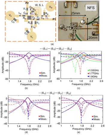
The layout, manufactured prototype, and utilized SMD components of NFS are depicted in Fig. 15(a). The capacitance tuning elements in the feedback are implemented using varactors (D1 and D2) in series with a DC block (CB) and a DC feed (RB). Figure 15(b) presents a comparison between the EM-simulated and RF-measured results of NFS, demonstrating good agreement and thereby validating the proposed concept. Specifically, the RF-measured performance at 1.77 GHz (bias state Vb = 0.763 V, Vc = 1.8 V) can be summarized as follows: 1.3 dB gain, 51 dB directivity, 9.4 dB NF, −7 dBm IIP3. Center-frequency tunability, which can be achieved by tuning the bias voltages of the transistor and the varactors in the coupled-line feedback, are shown in Fig. 15(c) with the following performance characteristics: center frequency tuning from 1.55 to 1.9 GHz, gain ranging from 0.3 to 1.3 dB, and directivity from 20 to 52 dB.
(a) Layout and photograph, (b) comparison of RF-measured and EM-simulated response, and (c) measured center frequency tuning response of the manufactured NFS prototype. (d) When ZS is 16 + j20 Ω, the measured S-parameters of the NFS after tuning Vf2 to 1.7 V. (e) When ZS is 23 − j12 Ω, the measured S-parameters of the NFS after tuning Vf2 to 3 V. The NFS components are listed as follows. T: BFU760F, D1 and D2: SMV1231-040LF, Rb = 511 Ω, Rc = 0 Ω, LB= 30 nH. CD = 220 μF, CB = 100 pF, R1 = 45.3 Ω, R2 = 4.5 Ω, R3 = 10 Ω, RB =10 MΩ, coupled line: W = 0.3 mm, S = 0.2 mm, L = 9 mm.

To experimentally validate the impedance matching capabilities of the NFS at its input port (P1), a de-embedding process was performed to move the reference plane at the input of NFS. Two different source impedances of 16 + j20 Ω and 23 − j12 Ω were considered and Fig. 15(d) and (e) illustrate the S-parameters of the NFS after tuning the capacitance of varactor D2 to obtain matching and high directivity. A comparison with the EM simulated results is also shown successfully validating the proposed adaptive NFS matching concept.
Figure 16(a) illustrates the layout and photograph along with the geometrical details of the three-stage BPFI (topology A), which comprises one NFS and two half-wavelength microstrip resonators. The RF-measured performance is summarized in Fig. 16(b) and (c). The comparison between the EM-simulated and the RF-measured S-parameter performance is provided in Fig. 16(b) and indicates good agreement, effectively validating the three-stage BPFI. At 1.77 GHz, the RF-measured performance can be outlined as follows: gain: −0.5 dB, directivity: 43 dB, NF: 11.3 dB, and IIP3: −7.3 dBm. The center-frequency tunability characteristics of the BPFI are shown in Fig. 16(c). It exhibits the following RF-measured characteristics: center frequency tuning from 1.52 to 1.9 GHz, gain ranging from −1.5 to −0.5 dB, and directivity from 20 to 44 dB. Especially, the directivity is 44 dB at the center frequency, while at 1.52 and 1.9 GHz, they are 42 and 20 dB, respectively.
(a) Photograph, (b) comparison of RF-measured and EM-simulated response, and (c) measured center frequency tuning response of the manufactured three-stage BPFI (topology A) prototype. Varactors in the passive resonator: MA46H072.

Figure 17(a) presents the photograph of the three-stage BPFI (topology C), consisting of one NFS, a half-wavelength microstrip resonator, and a multi-resonant microstrip resonator. Its measured performance at center frequency and tunability are summarized in Table 3 for brevity. To verify the impedance-matching capabilities of the BPFI, a de-embedding process was conducted to move the reference plane to the NFS input. Two distinct source impedances, 26 + j18 Ω and 26 − j14 Ω, were examined. Figure 17(b) and (c) depict the S-parameters of the BPFI after adjusting the capacitance of varactor D2 in NFS to achieve matching and high directivity. Additionally, a comparison with the EM simulated results is presented, effectively confirming the efficacy of the proposed adaptive BPFI matching concept. Tests with more source impedances were conducted, as depicted in Fig. 18. Specifically, Fig. 18(a) and (b) illustrate responses for Zs values of 14 + j20 Ω and 14 − j15 Ω, respectively. Furthermore, Fig. 18(c) provides an overview of all measured source impedances on a Smith Chart, distinguishing between those represented in Fig. 18(a) and (b) (green stars) and Fig. 17(b) and (c) (purple stars). Notably, these tests confirm the realization of imaginary part of admittance matching, consistent with simulated results in Fig. 12(a).
Manufactured three-stage BPFI (topology C) matching network. (a) Photograph. (b) RF measured and EM simulated response when ZS is 26 + j18 Ω. (c) RF measured and EM simulated response when ZS is 26 − j14 Ω.

RF measured response of Figure 17(a) when ZS is (a) 14 + j20 Ω and (b) 14 − j15 Ω. (c) Measured ZSs drawn in Smith Chart.

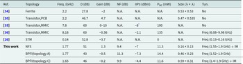
Comparison with state-of-the-art nonreciprocal RF filtering components
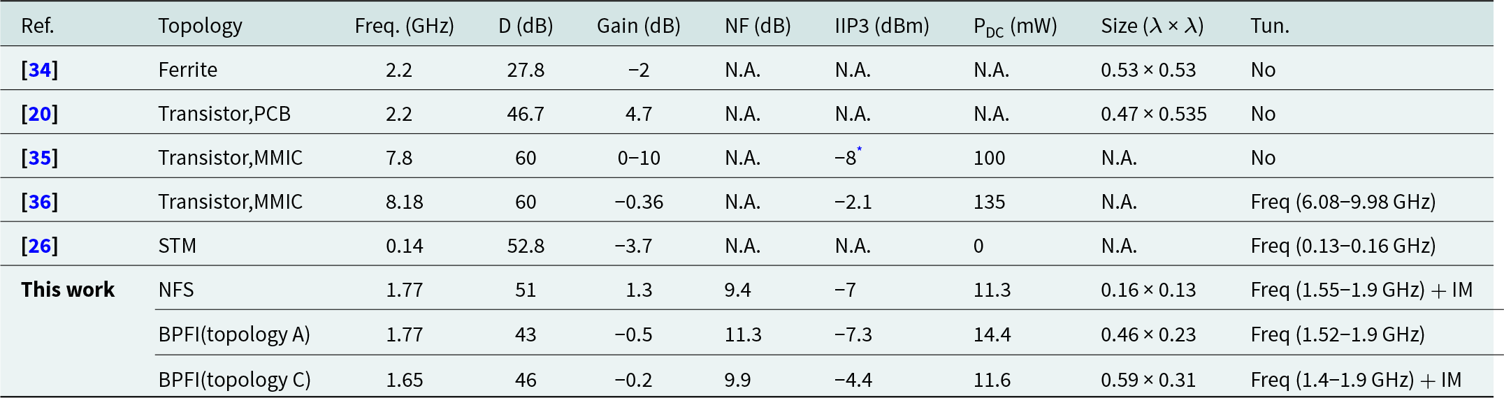
D: directivity; Filt.: filtering; Tun.: tenability; IM: impedance matching.
* estimated.
A comparison between the tunable NFS and nonreciprocal BPF concept with state-of-the-art nonreciprocal components is presented in Table 3. When compared with static ferrite-based filtering components [Reference Ashley and Psychogiou34], the proposed approach demonstrates higher directivity and gain, a smaller size, and tunability. The transistor-based BPFIs discussed in papers [Reference Ashley and Psychogiou20, Reference Simpson and Psychogiou35, Reference Simpson and Psychogiou36] exhibit higher power consumption. Specifically, when compared to the work in paper [Reference Ashley and Psychogiou20], this work demonstrates uniquely a tuning concept for center frequency as well as a tuning concept for adaptive impedance matching, whereas the devices in paper [Reference Ashley and Psychogiou20] is static. When comparing the proposed concept with STM-based BPFs, it operates at a higher operating frequency and has lower loss [Reference Simpson and Psychogiou26]. As indicated, the proposed NFS-based BPF concept is the only tunable transistor-based nonreciprocal component with integrated RF filtering functionality and adaptive matching network capabilities. The IIP3 performance of the proposed concept is comparable to the state-of-the-art and can be enhanced by adjusting the dimensions of the NFS or employing a higher biasing voltage for the transistor, as detailed in the “NFS design trade-offs” section.
Conclusion
This paper introduced a comprehensive design methodology of a new class of tunable multifunctional RF components with the co-integrated functionality of a tunable BPF, an RF isolator, and an adaptive matching network within a single RF component. The proposed tunable nonreciprocal BPFI concept is based on a miniaturized and tunable NFS comprising a transistor-based path and coupled-line feedback, which are incorporated within the filter volume along with frequency-tunable capacitively loaded microstrip resonators. The paper elaborated on the operational principles, design considerations, and impedance matching ability of the NFS, along with its application in high-stage frequency-tunable BPFI. Finally, experimental validation of an NFS and two three-stage BPFIs with frequency tunability and impedance matching ability were conducted at L band.
Funding statement
This work was supported by Science Foundation Ireland (SFI) under grants 20/RP/8334 and SFI-13/RC/2077.
Competing interests
The authors report no conflict of interest.

Kexin Li received the bachelor’s degree in communication engineering from Nanjing University of Science and Technology, Nanjing, China, in 2019, and the master’s degree in electromagnetic fields and microwave technology from Southeast University, Nanjing, China, in 2022. She is currently working toward the Ph.D. degree in Electrical and electronic engineering with the University College Cork, Cork, Ireland. Her main research focuses on the design of reconfigurable RF front-end components.

Dimitra Psychogiou received the Dipl.-Eng. degree in electrical and computer engineering from the University of Patras, Patras, Greece, in 2008, and the Ph.D. degree in electrical engineering from the Swiss Federal Institute of Technology (ETH), Zürich, Switzerland, in 2013. She is currently a Professor of Electrical and Electronic engineering with University College Cork (UCC) and the Head of the Advanced RF Technology Group, Tyndall National Institute, Cork, Ireland. Prior to joining UCC, she was a Senior Research Scientist with Purdue University, West Lafayette, IN, USA and an Assistant Professor with the University of Colorado Boulder, Boulder, CO, USA. Her research has been presented in more than 250 publications. Her current research interests include RF design and characterization of reconfigurable microwave and millimeter-wave passive components, RF-MEMS, acoustic wave resonator-based filters, tunable filter synthesis, frequency-agile antennas, and additive manufacturing technologies for 3D antenna subsystems. She is a Senior Member of URSI and a member of the IEEE MTT-S Filters and Passive Components (MTT-5) and Microwave Control Materials and Devices (MTT-13) committees. She has received multiple awards, including the 2023 IEEE MTT-S Outstanding Young Engineer Award, the 2021 Roberto Sorrentino Prize, the SFI Research Professorship Award, the 2020 NSF CAREER Award, the 2020 URSI Young Scientist Award, and the Junior Faculty Outstanding Research Award from UC Boulder. She is the Chair of MMT-13 and the Secretary of the USNC-URSI Commission D. She was an Associate Editor of the IET Microwaves, Antennas and Propagation. She is an Associate Editor of the IEEE Microwave and Wireless Components Letters and the International Journal of Microwave and Wireless Technologies. Furthermore, she serves on the technical review board for various IEEE and EuMA conferences and journals.


 Open access