

1 Introduction
Micro-structured foils have been intensively exploited in the last several years as targets for applications of ultra-high-power lasers in nuclear physics[ Reference Prencipe, Fuchs, Pascarelli, Schumacher, Stephens, Alexander, Briggs, Büscher, Cernaianu, Choukourov, De Marco, Erbe, Fassbender, Fiquet, Fitzsimmons, Gheorghiu, Hund, Huang, Harmand, Hartley, Irman, Kluge, Konopkova, Kraft, Kraus, Leca, Margarone, Metzkes, Nagai, Nazarov, Lutoslawski, Papp, Passoni, Pelka, Perin, Schulz, Smid, Spindloe, Steinke, Torchio, Vass, Wiste, Zaffino, Zeil, Tschentscher, Schramm and Cowan 1 ], proton radiography[ Reference Bulanov and Khoroshkov 2 ] and cancer therapy (hadrontherapy)[ Reference Schwoerer, Pfotenhauer, Jäckel, Amthor, Liesfeld, Ziegler, Sauerbrey, Ledingham and Esirkepov 3 ]. Theoretical and experimental studies have shown that, by irradiating structured and engineered targets, including gratings[ Reference Kahaly, Yadav, Wang, Sengupta, Sheng, Das, Kaw and Kumar 4 , Reference Ceccotti, Floquet, Sgattoni, Bigongiari, Klimo, Raynaud, Riconda, Heron, Baffigi, Labate, Gizzi, Vassura, Fuchs, Passoni, Květon, Novotny, Possolt, Prokůpek, Proška, Pšikal, Štolcová, Velyhan, Bougeard, D’Oliveira, Tcherbakoff, Réau, Martin and Macchi 5 ], nanowires[ Reference Jiang, Krygier, Schumacher, Akli and Freeman 6 , Reference Jiang, Ji, Audesirk, George, Snyder, Krygier, Poole, Willis, Daskalova, Chowdhury, Lewis, Schumacher, Pukhov, Freeman and Akli 7 ], nanoparticles[ Reference Dalui, Wang, Trivikram, Sarkar, Tata, Jha, Ayyub, Sheng and Krishnamurthy 8 ], nano-channels[ Reference Bailly-Grandvaux, Kawahito, McGuffey, Strehlow, Edghill, Wei, Alexander, Haid, Brabetz, Bagnoud, Hollinger, Capeluto, Rocca and Beg 9 , Reference Purvis, Shlyaptsev, Hollinger, Bargsten, Pukhov, Prieto, Wang, Luther, Yin, Wang and Rocca 10 ] and flat-top cones[ Reference Flippo, D’Humières, Gaillard, Rassuchine, Gautier, Schollmeier, Nurnberg, Kline, Adams, Albright, Bakeman, Michel, Johnson, Korgan, Letzring, Malekos, Renard-LeGalloudec, Sentoku, Shimada and Hegelich 11 ], with high-intensity laser pulses, novel processes and surface effects can be excited, which can enhance the radiation yield over a broad spectral range[ Reference Paul, Toma, Breger, Mullot, Augé, Balcou, Muller and Agostini 12 – Reference Kulcsár, Al Mawlawi, Budnik, Herman, Moskovits, Zhao and Marjoribanks 14 ] or improve the physical parameters of the electron and ion beams[ Reference Sgattoni, Fedeli, Cantono, Ceccotti and Macchi 15 – Reference Cantono, Sgattoni, Fedeli, Garzella, Réau, Riconda, Macchi and Ceccotti 17 ]. The modulations of the target surface induced by the laser pulse itself[ Reference Monchocé, Kahaly, Leblanc, Videau, Combis, Réau, Garzella, D’Oliveira, Martin and Quéré 18 ] or by target engineering are effective methods to maximize the laser energy coupling since various absorption mechanisms, for example, vacuum heating[ Reference Sumeruk, Kneip, Symes, Churina, Belolipetski, Donnelly and Ditmire 19 ], are sensitive to the laser field structure at the target surface[ Reference Klimo, Psikal, Limpouch, Proska, Novotny, Ceccotti, Floquet and Kawata 20 ]. Relativistic laser driven plasmas generated by solid targets have been shown to support the generation of intense radiation beams of energy over a wide range, from terahertz to X-ray. The electron bunches can be generated periodically during every laser cycle at the vacuum–plasma interface and their dynamics is relevant for the emission of electromagnetic radiation[ Reference Dromey, Rykovanov, Yeung, Hörlein, Jung, Gautier, Dzelzainis, Kiefer, Palaniyppan, Shah, Schreiber, Ruhl, Fernandez, Lewis, Zepf and Hegelich 21 , Reference Liao, Li, Li, Su, Zheng, Liu, Wang, Hu, Yan, Dunn, Nilsen, Hunter, Liu, Wang, Chen, Ma, Lu, Jin, Kodama, Sheng and Zhang 22 ]. Recently, experimental and numerical results indicate that nano-structured targets enable the control of the electron bunch dynamics and, consequently, the properties of the emitted electromagnetic radiation[ Reference Mondal, Wei, Fareed, Hafez, Ropagnol, Sun, Kahaly and Ozaki 23 ].
Micro-gratings with periodic ordered surface structures have been of particular interest for the high-power laser community, aiming to improve the physical parameters of the laser driven particle and radiation sources[ Reference Ceccotti, Floquet, Sgattoni, Bigongiari, Klimo, Raynaud, Riconda, Heron, Baffigi, Labate, Gizzi, Vassura, Fuchs, Passoni, Květon, Novotny, Possolt, Prokůpek, Proška, Pšikal, Štolcová, Velyhan, Bougeard, D’Oliveira, Tcherbakoff, Réau, Martin and Macchi 5 , Reference Cantono, Sgattoni, Fedeli, Garzella, Réau, Riconda, Macchi and Ceccotti 17 , Reference Margarone, Klimo, Kim, Prokůpek, Limpouch, Jeong, Mocek, Pšikal, Kim, Proška, Nam, Štolcová, Choi, Lee, Sung, Yu and Korn 24 – Reference Gheorghiu, Ionescu, Ghenuche, Cernaianu, Doria, Popa and Leca 30 ]. Recent studies demonstrated that surface plasma waves (SPWs) can be resonantly excited on micro-gratings with periodic surface structures and irradiated by high-intensity laser pulses[ Reference Ceccotti, Floquet, Sgattoni, Bigongiari, Klimo, Raynaud, Riconda, Heron, Baffigi, Labate, Gizzi, Vassura, Fuchs, Passoni, Květon, Novotny, Possolt, Prokůpek, Proška, Pšikal, Štolcová, Velyhan, Bougeard, D’Oliveira, Tcherbakoff, Réau, Martin and Macchi 5 , Reference Sgattoni, Fedeli, Cantono, Ceccotti and Macchi 15 – Reference Cantono, Sgattoni, Fedeli, Garzella, Réau, Riconda, Macchi and Ceccotti 17 ]. Moreover, thin foils of μm thickness with periodically modulated structures on their surface allow the investigation of laser driven particle beams in a wider spatial and angular range, compared with bulk grating targets (e.g., Ref. [Reference Ceccotti, Floquet, Sgattoni, Bigongiari, Klimo, Raynaud, Riconda, Heron, Baffigi, Labate, Gizzi, Vassura, Fuchs, Passoni, Květon, Novotny, Possolt, Prokůpek, Proška, Pšikal, Štolcová, Velyhan, Bougeard, D’Oliveira, Tcherbakoff, Réau, Martin and Macchi5]). These kinds of observations are possible due to the μm transverse dimension of the target, which allows investigations over (almost) the full angular range around the interaction point. One may note that these effects can be obscured by the intrinsic temporal profile of high-intensity laser pulses[ Reference Giesecke, Peth, Toncian, Willi and Cerchez 27 , Reference Hidding, Pretzler, Clever, Brandl, Zamponi, Lübcke, Kämpfer, Uschmann, Förster, Schramm, Sauerbrey, Kroupp, Veisz, Schmid, Benavides and Karsch 31 – Reference Chu, Liang, Yu, Xu, Xu, Ma, Lu, Liu, Leng, Li and Xu 35 ]. A target will always be irradiated prior to the main peak by the relatively low-intensity, nanosecond background (amplified spontaneous emission) and pre-pulses and, thus, a preplasma will be created with a spatial expansion of the order of micrometres. In the case of micro- and nano-scale structured targets, the preplasma expansion can reach similar characteristic lengths to the surface modulations and, thus, can limit the physical surface effects. Various laser pulse cleaning techniques have been developed, such as nonlinear temporal filters based on cross-polarized wave generation (XPW module)[ Reference Jullien, Albert, Burgy, Hamoniaux, Rousseau, Chambaret, Augé-Rochereau, Chériaux, Etchepare, Minkovski and Saltiel 36 ] or single- and double-plasma systems[ Reference Ziener, Foster, Divall, Hooker, Hutchinson, Langley and Neely 37 , Reference Dromey, Kar, Zepf and Foster 38 ], which can significantly minimize the preplasma expansion down to tens of nm scale length.
Conventional metallic gratings are commonly fabricated on a substrate (e.g., glass, polymer, silicon) by means of nanoimprinting[ Reference Bhushan 39 ] or by lithographic methods (e.g., interference lithography[ Reference Rodriguez, Echeverría, Ellman, Perez, Verevkin, Peng, Berthou, Wang, Ayerdi, Savall and Olaizola 40 ], deep ultraviolet lithography[ Reference Bratton, Yang, Dai and Ober 41 ], electron or ion beam lithography[ Reference Kim, Ahn and Jang 42 ] and multiphoton lithography technique or direct laser writing[ Reference Kowalczyk, Nawrot and Zinkiewicz 43 ]). These techniques are intended for structuring the photosensitive material covering the substrate, which is commonly followed by a physical[ Reference Shi, Lu, Lu, Wang, Qi, Xu and Chi 44 ] or chemical etching process[ Reference Jiao, Gao, Zhang, Xie, Zhou, Zhang, Zhang, Gao, Luo, Wu, Zhu, Zhang, Liu, Mu, Yang and Gu 45 ], and lastly coating the resulting patterned substrate with the desired metal (e.g., by sputter deposition[ Reference Kumari, Mohapatra and Moirangthem 46 ], thermal evaporation[ Reference Lütolf, Martin and Gallinet 47 ] or chemical vapor deposition[ Reference Hirai, Ushiro, Kanakugi and Matsuura 48 ]). A low-cost fabrication method for metallic gratings (gold gratings on glass substrate) was reported by Hirai et al. [ Reference Hirai, Ushiro, Kanakugi and Matsuura 48 ]. They eliminated the deposition step by using direct imprint lithography at room temperature (RT) into the gold layer, allowing its plastic deformation and thus revealing the gold structures. Despite the high uniformity of the patterns over a relatively large area (up to 2 mm in width), the pattern size obtained by this method is significantly limited to the imprint pressure, which above 1000 MPa fractures the sample. Rodriguez et al. [ Reference Rodriguez, Echeverría, Ellman, Perez, Verevkin, Peng, Berthou, Wang, Ayerdi, Savall and Olaizola 40 ] showed that laser interference lithography can be used for patterning on a micrometre-scale of oxidized silicon wafer, up to 3 inches in diameter. Using nanoimprint lithography, Shi et al. [ Reference Shi, Lu, Lu, Wang, Qi, Xu and Chi 44 ] obtained rectangular metallic nano-structures on silicon substrates by means of a single micro-scale stamp. Adjusting the imprinting process parameters allowed a wide range of nano-structures with controlled widths and heights, maintaining the quality and the shape of the patterns, down to a few tens of nanometres resolution limit. Fabrication of periodic metallic gratings on a large area was reported by Kumari et al. [ Reference Kumari, Mohapatra and Moirangthem 46 ], the grating template being nanoimprinted into a polymer covering a glass substrate that, after a gold sputter deposition step, leads to metallic gratings. Their procedure, while cost-efficient, has a major limitation, namely that it can be used only for supported films.
To our knowledge, micrometre-sized gratings fabricated directly into thin (less than 10 μm) un-supported metallic foils have not been previously reported. The strategy presented in this paper is a novel approach for the production of periodic gratings of one micrometre lateral size, comparable to the Extreme Light Infrastructure Nuclear Physics (ELI-NP) laser wavelength (λ ~ 0.8 μm). Typical semiconductor manufacturing techniques have been used in order to obtain gratings with rectangle and sinusoidal-like shapes. Several issues were addressed, such as handling difficulties, as the foil is self-supporting and easily bends, the need of the foil pre-processing before patterning and the optimization of the engraving processes. The micro-grating patterns are etched directly into the metallic foils by means of electron-beam lithography (EBL) and dry-plasma etching (Ar-ion milling), common techniques for most micro/nano-fabrication laboratories. By combining the Ar-ion milling process with the sample rotation and tilt, different geometries and shapes of gratings can be achieved.
2 Experimental details
2.1 Materials and methods
Commercial gold (Au) and copper (Cu) foils produced by Goodfellow of 10 μm thickness, 25 mm × 25 mm size, 99.9% purity, were used in this work. Dry etching for surface cleaning and resist removal, where applicable, was performed using a controlled bombardment with Ar+ ions, by means of an Ar-ion milling unit (Kaufmann ion source, KDC160 model). The milling unit is part of an ultra-high vacuum sputter deposition system[ Reference Gheorghiu, Leca, Popa, Cernaianu and Stutman 49 ], with a background pressure of the vacuum chamber of approximately 2 × 10⁻⁸ mbar. The ion milling processes were performed at a pressure of 5 × 10⁻⁴ mbar Ar (2 sccm Ar), a beam current of 100 mA, 90 V beam acceleration, 450 V beam voltage and 7 r/min sample holder rotation (to ensure good uniformity of the milling process over the foil area and to reduce the shadowing effect). Thus, an etching rate of approximately 20 nm/min for Au and approximately 25 nm/min for Cu was obtained. Constructively, the Ar-ion milling source is placed below the sample position, at an angle of 45° from the horizontal. Consequently, two strategies have been used: (i) a horizontal holder plate, which by means of the equipment configuration will result in a 45° angle of incidence of the Ar ions with respect to the surface of the sample; and (ii) a correction of that configuration via a 45° support for the metallic foils, giving a perpendicular direction of the ions on the surface of the samples during etching. Plasma etching was also used as part of the resist removal tests, with the process performed by a reactive ion etching system (PlasmaPro Estrelas100 model, Oxford Instruments Plasma Technology) using a high-frequency (HF) generator at 100–300 W, or an inductively coupled plasma (ICP) unit at 500–2500 W.
In different stages of the fabrication process, the samples were analysed by scanning electron microscopy (SEM; MAIA3 model, from Tescan) using a secondary electron detector and 30 kV accelerating voltage of the electron beam. An electron backscatter diffraction (EBSD) system with a Bruker e-Flash1000 detector was used for micro-structural studies (crystal orientation and grain size distribution), while an EBL unit (from Tescan) was used for surface structuring. For the EBSD analysis, the samples were mounted on an Al stage tilted at 70°, at a detector distance of 18 mm, with the diffracted backscattered signal being collected on a phosphor screen (scintillator); Esprit 2.1 software was used to analyse the obtained EBSD data. Monte Carlo simulations were performed with the Casino V 2.42 software package (‘Monte Carlo Simulation of electron trajectory in sOlids’). Besides electron microscopy, the grating characteristics (shape, roughness, spacing, periodicity) and the resist thickness were investigated using atomic force microscopy (AFM; NTEGRA model, from NT-MDT), with a whisker-type carbon tip (11.5 N/m force constant, 255 kHz resonant frequency, tip curvature radius 10 nm, tip length 1 μm). An optical overview of the samples was performed using a Nikon optical microscope, in bright and dark field modes.
2.2 Micro-grating fabrication
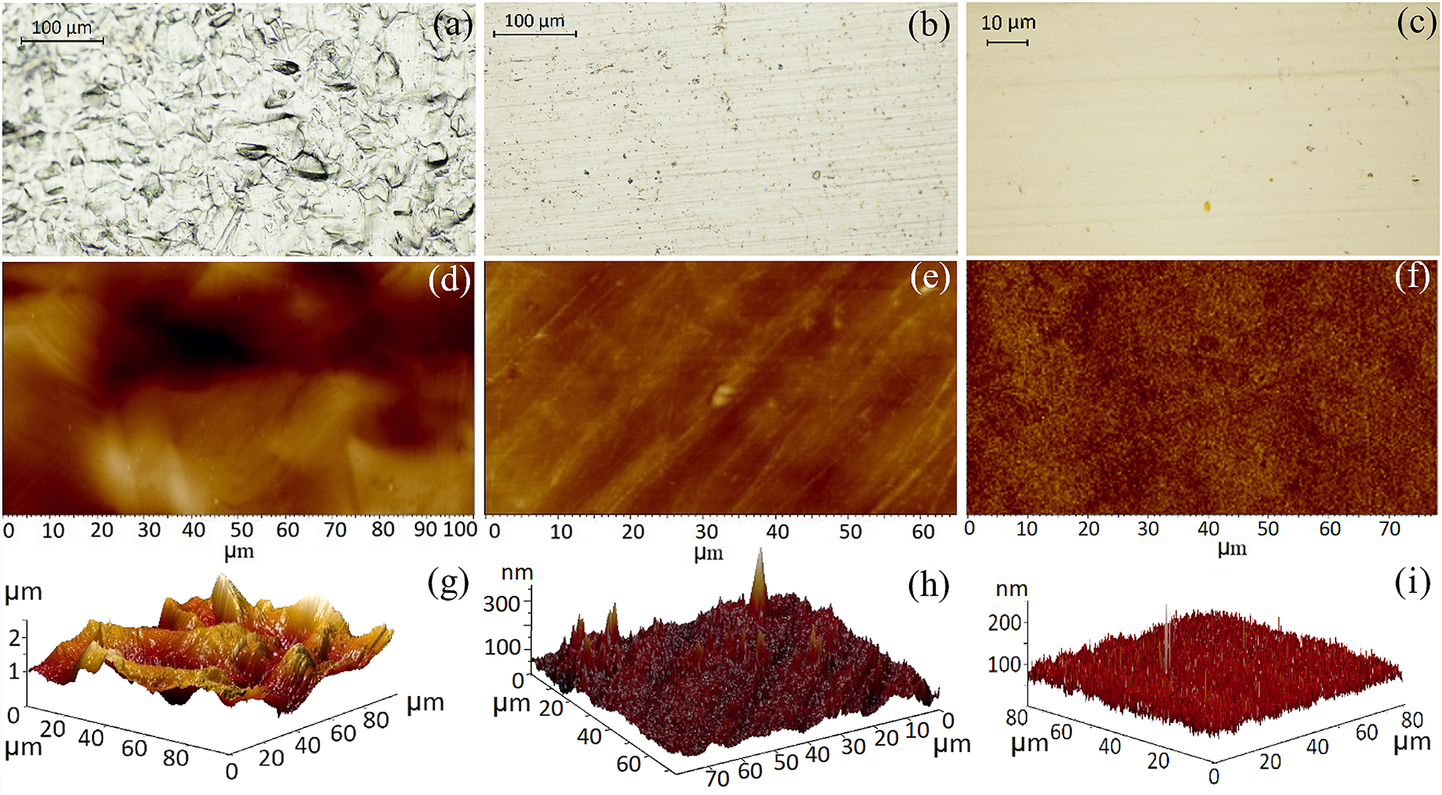
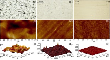
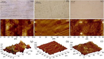
Before any processing, the metallic foils were thoroughly cleaned with acetone and rinsed with isopropanol to remove any organic impurities and dissolve the contaminants present on the surface of the foils, and then dried using compressed air (dry and oil-free). Following the solvent cleaning, the foils were subjected to cold rolling in order to improve the roughness and flatness of their surface and then dry cleaned by means of Ar-ion milling to efficiently decontaminate both surfaces of the foils. The milling process was performed for 20 min (in sequences of 1 min beam ON/1 min beam OFF, to allow for sample cooling) for each side of the foil. The evolution of the foil surface topography after each process (as-received, cold rolled and Ar-ion milled) is shown in Figure 1 for Au and in Figure 2 for Cu. For this, optical microscopy (Figures 1(a)–1(c) and Figures 2(a)–2(c)) and AFM analysis, including 2D (Figures 1(d)–1(f) and Figures 2(d)–2(f)) and 3D imaging (Figures 1(g)–1(i) and Figures 2(g)–2(i)), were performed. The results of the roughness profile measured by AFM are summarized in Table 1, as root mean square (RMS) values.
(a)–(c) Optical images, (d)–(f) 2D AFM images and (g)–(i) 3D AFM images of Au foils: (a), (d), (g) as-received, (b), (e), (h) after cold rolling and (c), (f), (i) after surface cleaning by Ar-ion milling.
RMS roughness obtained by AFM analysis of as-received and processed metallic foils.

(a)–(c) Optical images, (d)–(f) 2D AFM images and (g)–(i) 3D AFM images of Cu foils: (a), (d), (g) as-received, (b), (e), (h) after cold rolling and (c), (f), (i) after surface cleaning by Ar-ion milling.
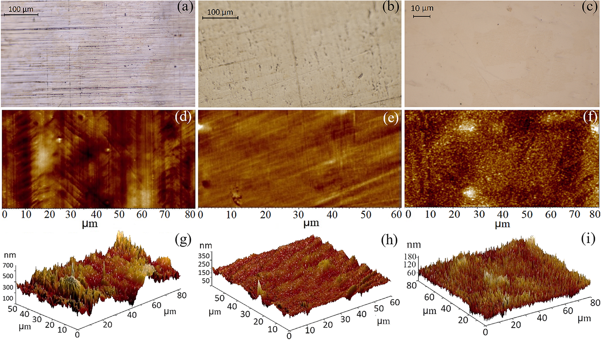
The optical (Figure 1(a)) and AFM (Figures 1(d) and 1(g)) images show that the as-received Au foils were characterized by a rough topography, with peak-to-valley values of up to 2 μm. A significant improvement of the roughness occurred after cold rolling, as indicated by the optical (Figure 1(b)) and AFM images (Figures 1(e) and 1(h)), results sustained by the evolution of RMS values, which for the as-received and cold rolled foils were 350 and 20 nm, respectively. A further, smaller improvement in roughness was observed after the Ar-ion milling process (see Table 1), with an RMS value of about 13 nm for the etched Au foil. For Cu foil the cold rolling process was found to be less critical, with RMS values of 88 nm for the as-received Cu foil and 34 nm after the cold rolling process, with a further decrease in roughness to 21 nm after dry etching. The evolution of the surface morphology for a Cu foil is shown in Figure 2, from the as-received (Figures 2(a), 2(d) and 2(g)), through cold rolling (Figures 2(b), 2(e) and 2(h)), to the final dry etched surface (Figures 2(c), 2(f) and 2(i)). These results showed that the use of cold rolling, as part of the fabrication procedure, proved to be a crucial step, with a significant decrease in foil roughness and flatness, especially for the Au foils.
After the Ar-milling cleaning step, the foils were temporarily fixed onto a 1-inch Si wafer in order to facilitate the handling and to avoid their wrinkling. A positive-tone PMMA A8 EBL resist (poly-methyl methacrylate/C5H8O2, EM Resist Ltd., 9.5 × 10⁵ molecular weight, 8% mass fraction in anisole) was then spin-coated on the surface of the foil (at 4000 r/min, for 45 s) to a thickness of about 600 nm. The resist was next baked on a hot plate at 180°C, for 3 min in order to dry and harden the coated resist and improve its adhesion to the foil. Subsequently, the samples were mask-free exposed to the electron beam following the digital patterns of the gratings created with Drawbeam Advanced Software. The exposure was performed at 30 kV accelerating voltage, 300 μC/cm2 e-beam dose and 450 μm × 450 μm write field. To reveal the structures by removing the exposed resist, the samples were developed in a 1:3 4-methyl-2-pentanone (MIBK)/isopropyl alcohol (IPA) solution for 2 min at 22°C, then 30 s in 1:9 MIBK/IPA solution, and rinsed in pure IPA for 30 s to terminate the resist developing process, preventing the formation of residues on the surface. The samples were then dried with compressed air and baked for 60 s at 100°C in order to chemically and thermally stabilize the resist structures for the subsequent dry-plasma etching process. Ar-ion milling was then used to transfer the patterns to the foils, thus creating grating-like structures by removing material from the areas exposed to the electron beam. As a result of the patterning process, nine 450 μm × 450 μm field structures containing the periodic gratings were obtained on each free-standing metallic foil, with 5 mm distance between them; the separation is required in order to avoid damaging neighbouring structures during the high-power laser experiments. In addition, each foil was engraved with an identification marker (for structure position and orientation recognition) and with an identification text. Finally, the metallic foil was released from the support wafer and a milling process of the rear side of the free-standing patterned foil was performed.
3 Results and discussion
3.1 Optimization of lithographic and etching processes
During cold rolling and Ar-ion milling processes, the foils suffer micro-structural changes due to mechanical and thermal stresses that may affect the mechanical strength of the foils[ Reference Wu, Li, He, Zhao and Zhan 50 , Reference Pham, Thuillier and Manach 51 ]. Therefore, in order to determine the modifications of the material micro-structure due to these processes, the surfaces of the foils are analysed using the EBSD technique. For the as-received Au foils the crystalline orientation maps showed a non-preferred orientation of the grains, while after the cold rolling process a <001> preferred orientation is observed. Following the etching step, the inverse pole figure (IPF) map suggests that this process induces also the <111> orientation, additionally to the <001> direction, thus reverting to the initial crystalline orientations of the as-received foils. This change in the surface orientation may be due to the recrystallization process of the damaged surface layer, which occurs during sample cooling down after etching by Ar-ion milling. It can also indicate a post-cold rolling stress release mechanism through heating during the milling process, the foils reaching temperatures of at least 200ºC during Ar-ion milling. In contrast, in the Cu foils, the random crystallographic orientation of the as-received foil is maintained after cold rolling and Ar-ion milling, an indication of less or no influence on the surface micro-structure of these processes. Grain distribution maps and histograms show an equiaxed micro-structure in the case of Au foils (4 μm average grain diameter), whereas for Cu foils larger and elongated grains are observed (8 μm average diameter). A detailed description of the EBSD data is given in the Supplementary Materials.
As part of the optimization process, Monte Carlo simulation and preliminary tests were used to determine the key parameters (e.g., acceleration voltage, exposure dosage, beam step size) of the electron-beam lithographic procedure. The computation data provided the interaction, scattering and penetration depth of the incident electrons in different substrate materials (Au, Cu and, for comparison purposes, also Si). This study brought relevant information related to the quality of the grating’s edges, as a deep undercut and blurred margins of the pattern profile are expected in the case of metallic substrates. Substrates with a high atomic number (e.g., Au) showed a reduced interaction volume and penetration depth of the primary electrons in the PMMA resist, but with widening of the forward scattered electrons. Moreover, the number and spread of the backscattered electrons increase significantly, leading to an additional exposure of the resist, hence blurry, more irregular edges. Further, calculations of the electron backscatter coefficient showed that a more pronounced proximity effect phenomenon is observed in the case of the Au substrate, leading to distorted edges. Monte Carlo simulations of the absorbed energy revealed, for complete exposure of a 600 nm thick PMMA layer, an optimum doze of 300 μC/cm2 and 30 nm step size, for an electron-beam energy of 30 keV and 18.5 nm beam radius. Details of the Monte Carlo simulations are given in the Supplementary Materials.
In order to determine the appropriate parameters for the resist development process, for example, development time, developer dilution and temperature, several tests have been carried out followed by optical analysis of the obtained structures. During the electron exposure, the PMMA resist suffers a chain scission of its long chain molecule by breakdown into short low-molecular-weight fragments, which are susceptible to dissolution in an optimum developer solution. Therefore, the development process is mainly influenced by the exposure dose, temperature and development time. The results show that for a complete development and clearance of the PMMA resist in the exposed areas, a mixture of 1:3 MIBK/IPA (for 120 s) is necessary, followed by 1:9 MIBK/IPA solution (for 30 s) and rinsing in pure IPA (for 30 s) to terminate the developing process. All steps were performed at RT.
During the dry etching process, the PMMA resist suffers degradation with the formation of covalent bonds between the short, divided fragments. Due to its higher degree of crosslinking (interlinking the polymer chains by covalent bonds) and its graphitization, when formation of carbon double bonds is favoured, the resist becomes harder to remove. According to the degradation mechanism of the PMMA resist during the ion etching process[ Reference Koval and Vac 52 ], the polymer layer modifies from its initial form to low-molecular-weight chain scission, to crosslinking, finally converting to a graphitized material at high temperature.
An important step addressed in this study was the removal of the hardened resist resulting from the etching process of the gratings by Ar-ion milling, the resist removal being directly correlated with the quality of the final structures. In this matter, several methods have been approached in order to compare and identify the most suited one for our resist type, pattern characteristics and experimental conditions. Physical methods, such as Ar-ion milling and plasma etching in a reactive-ion etching (RIE) system (oxygen and argon plasma), or chemical methods, including several stripper solutions, have been considered (see the Supplementary Materials). From the tested methods, the Ar-ion milling process was found to give the best results, leading to complete removal of the hardened PMMA resist, while keeping the high-quality aspect of the gratings, thus being used further on in the micro-gratings processing. Details of the efficiency of each physical and chemical method are given in the Supplementary Materials. For achieving periodic gratings with 1 μm lateral dimension and 1 μm spacing, several process parameters of Ar-ion milling were optimized, the most important being the etching and cooling times. Gratings for which the etching process has not been properly optimized are shown in Figure 3. A too short etching time proved to give wider etched areas and very narrow non-etched zones, as shown in Figure 3(a) for Cu and in Figure 3(b) for Au gratings. The images indicate etched structures having a triangular-like shape, but not with the intended periodicity. These results can be understood considering the complete removal of the resist along with partial removal of the metallic gratings, with a higher etching rate of the material from the top of the gratings, as compared with the etching rate of the grating side walls. This difference in etching rates between the top and lateral sides of the gratings is due to different exposure time to the plasma during sample rotation, with longer exposure time of the top side.
SEM images of micro-gratings using an unoptimized dry etching (Ar-ion milling) process: (a) Cu gratings, 9 min dry etching; (b) Au gratings, 20 min dry etching; (c) Cu gratings, 25 min dry etching; (d) Au gratings, 40 min dry etching; (e) Au gratings, 18 min dry etching + 10 min P1316 solution (RT); (f) Cu gratings, 9 min dry etching + 5 min P1316 solution (90°C); (g) Au gratings, 20 min dry etching, without foil cold rolling. For (f), dry etching was done perpendicularly to the surface, and at 45° to the sample normal for the rest.

Another critical etching process parameter that affected the grating quality was the cooling time during Ar-ion milling, with a too short cooling time (sequences of 1 min ON/30 s OFF) leading to sample overheating problems. This results in crystallization and further hardening of the resist on the surface, thus damaging the quality of the gratings, as indicated in Figure 3(c) for Cu and Figure 3(d) for Au foils. Also, for an optimized patterning process, the resist had to be completely removed during dry etching, as the chemical etching showed little effect in removing the (hardened) resist. Examples of inefficient removal of the resist by chemical etching (P1316 solution at RT or heated at 90°C) are shown in Figures 3(e) and 3(f), where the poor efficiency in completely removing the remaining resist and the deleterious effect on gratings can be observed. Note that different etching times and different sample tilts have been used for these two samples. The incident angle of the Ar+ ions to the sample surface has a significant effect not only on the final etching profile, but also on the etching rate and on the damage of the resist, affecting the grating quality[ Reference Wolff, Lägel and Trellenkamp 53 ]. For incident angles close to the surface normal, the number of defects (e.g., bubbles, holes) can be significantly decreased.
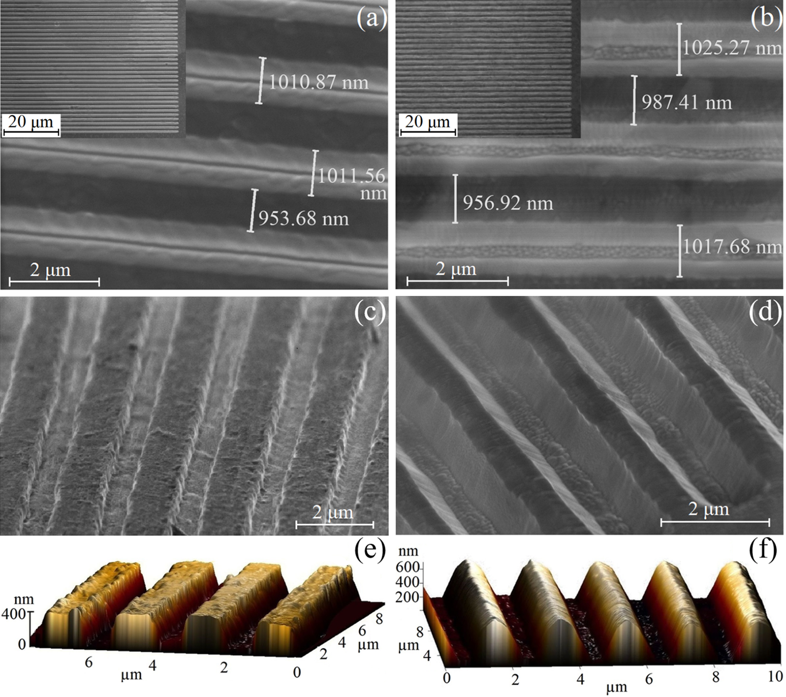
SEM images of grating patterns in (a) Cu and (b) Au foils obtained after the complete optimized fabrication process; darker parts correspond to non-etched areas and brighter parts to etched areas. Insets show an overview of the gratings. (c), (d) SEM and (e), (f) AFM images with (c), (e) Cu rectangular and (d), (f) Au sinusoidal (trapezoidal) shape gratings.
Besides the etching parameters, one has to point out the importance of foil pre-processing; an example of gratings obtained on the as-received Au foil where no preliminary cold rolling process has been performed is shown in Figure 3(g). The irregular micrometre-size roughness and flatness of the as-received foils overcome the periodic sub-micrometre depth size patterning, giving a random, ineffective effect, where the large surface corrugations of the as-received Au foils overwhelm the patterning effect.
3.2 Optimized micro-patterns on free-standing metallic foils
Using the optimized parameters established for the EBL process and for the resist removal procedures, well-defined grating micro-structures have been engraved on self-supporting Au and Cu foils. As shown in Figure 4, 2 μm periodic grating patterns have been obtained for both metallic foils, with about 970 nm grating width and 1010 nm spacing (etched zones). Due to the difference in etching rates of Cu and Au, with a higher etching rate for Cu, some clear differences are noted on the etched areas. For the same etching time (30 min effective etching time, in sequences of 1 min beam ON/1 min beam OFF) a ‘V’ shape of the etched areas is obtained for the Cu foil (Figure 4(a)), whereas an inversed trapezoidal shape is obtained for Au foil (Figure 4(b)). A different structure of the side walls is also observed for the two materials: a saw-like structure for Cu and a flat one for Au. The structure of the side walls is an imprint of the resist edge shape resulting from the lithographic process, with slight waviness in the case of the Cu foils.
Different shapes of gratings can be obtained by varying the etching angle (the angular position of the sample surface with respect to the plasma), which has a leading effect on the geometry of the patterns. At normal incidence (perpendicular direction of the Ar ions to the sample surface), a rectangular profile of the metallic gratings was observed, with vertical walls; SEM and AFM images of such Cu gratings are shown in Figures 4(c) and 4(e), respectively. At 45° angle of incidence a sinusoidal-like profile was obtained, due to shadowing effect of the resist and gratings; examples of the resulting structures are shown in Figures 4(d) (SEM image) and 4(f) (AFM image), for Au foil. From AFM analysis, the gratings profile shows 2 μm periodicity and peak-to-valley amplitude of about 400 nm.
An essential aspect of high-power laser facilities that could represent a limiting factor in exploiting their full potential is the large number of targets required for high-repetition rate experiments, since they are destroyed after each shot[ Reference Prencipe, Fuchs, Pascarelli, Schumacher, Stephens, Alexander, Briggs, Büscher, Cernaianu, Choukourov, De Marco, Erbe, Fassbender, Fiquet, Fitzsimmons, Gheorghiu, Hund, Huang, Harmand, Hartley, Irman, Kluge, Konopkova, Kraft, Kraus, Leca, Margarone, Metzkes, Nagai, Nazarov, Lutoslawski, Papp, Passoni, Pelka, Perin, Schulz, Smid, Spindloe, Steinke, Torchio, Vass, Wiste, Zaffino, Zeil, Tschentscher, Schramm and Cowan 1 ]. Therefore, producing multiple gratings areas on the same metallic foil may provide the advantage of multiple shots. Besides the production of the targets, typically with multiple rigorous steps and often combining different techniques, as shown above, target micro-assembling and mounting in the final target holder are also part of the fabrication process and need to be considered. The mounting frame presented in Figure 5 allows the target positioning in the laser focal plane for nine targets, without an additional alignment procedure between shots. For high-repetition rate experiments, the micro-gratings can be produced on larger foils and sustained by similar frames of a corresponding size or can be fabricated in a large number on thin tapes and can be positioned in the interaction spot by tape-targets. As thin target, the micro-gratings operating as high repetition rate targets face a number of challenges, such as precision of the spatial positioning, reproducible parameters in the manufacturing process over large material areas, customization, handling, debris, and target surrounding activation. Currently, various target prototypes are proposed[ Reference Prencipe, Fuchs, Pascarelli, Schumacher, Stephens, Alexander, Briggs, Büscher, Cernaianu, Choukourov, De Marco, Erbe, Fassbender, Fiquet, Fitzsimmons, Gheorghiu, Hund, Huang, Harmand, Hartley, Irman, Kluge, Konopkova, Kraft, Kraus, Leca, Margarone, Metzkes, Nagai, Nazarov, Lutoslawski, Papp, Passoni, Pelka, Perin, Schulz, Smid, Spindloe, Steinke, Torchio, Vass, Wiste, Zaffino, Zeil, Tschentscher, Schramm and Cowan 1 ], aiming at solutions for reliable and secure multi-shot, high-repetition rate thin foil targets.
Al holder with patterned Cu foil for assembly demonstration purposes: (a) back side; (b) front side with overlaid dark field optical image of the nine grated areas; (c) side view; (d) cross-section view.

In order to be used as targets in high-power laser experiments, the final patterned foils have been removed from the supporting 1-inch Si wafer. After a cleaning step of the back side by Ar-milling, the obtained free-standing foils have been mounted on a custom-made Al holder, as depicted in Figure 5, for their further employment in high-power laser experiments. The holder design allows a sequence of 450 μm × 450 μm individual laser–grating interaction areas, allowing for several laser shots without the need for changing the sample during the experiment.
In addition, in experiments where the full angular monitoring of the interaction is required (e.g., in the investigation of the spatial distribution of the high-energy particle beams or plasma emission on the rear side of the target) the target holder can be removed. In this case, the micro-grating area can be individually mounted on a fine post, such as wire or thin capillary. Regarding the individual target mounting and assembly, several stalk geometries of different material compositions, for example, a cylindrical bar, sinusoidally modulated stalk or a spiral design, of aluminium or plastic materials, can be used. The modulated and spiral type stalks show the advantage of significantly reducing the electromagnetic pulse (EMP), which may damage the electronic equipment[ Reference Bradford, Woolsey, Scott, Liao, Liu, Zhang, Zhu, Armstrong, Astbury, Brenner, Brummitt, Consoli, East, Gray, Haddock, Huggard, Jones, Montgomery, Musgrave, Oliveira, Rusby, Spindloe, Summers, Zemaityte, Zhang, Li, McKenna and Neely 54 ].
3.3 Test experiments demonstrating the usability of the micro-gratings for laser–plasma applications
Thin targets with a periodically modulated surface have been previously investigated experimentally and theoretically, revealing superior physical properties of the accelerated particle beams following the irradiation by high-intensity laser pulses. For example, different studies indicate an enhancement of the cut-off energy and flux of protons accelerated by structured targets of different geometries[ Reference Klimo, Psikal, Limpouch, Proska, Novotny, Ceccotti, Floquet and Kawata 20 , Reference Margarone, Klimo, Kim, Prokůpek, Limpouch, Jeong, Mocek, Pšikal, Kim, Proška, Nam, Štolcová, Choi, Lee, Sung, Yu and Korn 24 ]. The explanation for the results mostly pointed towards a higher laser energy absorption by the structured targets[ Reference Andreev and Platonov 32 , Reference Cerchez, Swantusch, Toncian, Zhu, Prasad, Toncian, Rödel, Jäckel, Paulus, Andreev and Willi 33 ] and, consequently, to an increase of the hot electron population. Moreover, in the case of grating target (GT) geometry, the surface plasmon excitation was considered to explain the increased laser absorption and the proton cut-off energy for a laser incidence angle close to the plasmon resonance angle[ Reference Ceccotti, Floquet, Sgattoni, Bigongiari, Klimo, Raynaud, Riconda, Heron, Baffigi, Labate, Gizzi, Vassura, Fuchs, Passoni, Květon, Novotny, Possolt, Prokůpek, Proška, Pšikal, Štolcová, Velyhan, Bougeard, D’Oliveira, Tcherbakoff, Réau, Martin and Macchi 5 , Reference Liu, Tripathi, Shao and Liu 55 ].
The fabricated gratings presented in this work have been employed in experimental tests at the Arcturus laser system, Düsseldorf, Germany, investigating various physical processes, such as the coupling efficiency of the laser energy by the GTs or acceleration of high-energy particle beams (electrons and ions). The laser system can generate pulses with energies up to 7 J before compression at the central wavelength of $\lambda$
= 800 nm and a pulse duration of 30 fs (full width at half maximum, FWHM) in a p-polarization geometry. After the compression, the pulse is guided through a vacuum transport line with an energy efficiency of about 50%. At the entrance of the interaction chamber, the laser beam has a diameter of about 10 cm and is focused by an off-axis parabola (F# 2). Within the focal spot of about 5 μm diameter, 50% of the laser energy is contained, while 80% of the energy is focused within a diameter of about 9 μm. Hence, the target is irradiated with a short laser pulse of an intensity of the order of 1020 W/cm2.
$\lambda$
= 800 nm and a pulse duration of 30 fs (full width at half maximum, FWHM) in a p-polarization geometry. After the compression, the pulse is guided through a vacuum transport line with an energy efficiency of about 50%. At the entrance of the interaction chamber, the laser beam has a diameter of about 10 cm and is focused by an off-axis parabola (F# 2). Within the focal spot of about 5 μm diameter, 50% of the laser energy is contained, while 80% of the energy is focused within a diameter of about 9 μm. Hence, the target is irradiated with a short laser pulse of an intensity of the order of 1020 W/cm2.
The temporal profile of the laser pulse is managed by two stages implemented in the laser architecture, namely an XPW module in the front end and a single-plasma mirror system after the main amplifier. Thus, the pulse contrast is improved up to 10–12 in hundreds of picoseconds and to 10–9 in a few picoseconds before the pulse peaks. Previous experimental and numerical studies confirm a preplasma expansion in the range of tens of nm before the main interaction[ Reference Giesecke, Peth, Toncian, Willi and Cerchez 27 , Reference Cerchez, Giesecke, Peth, Toncian, Albertazzi, Fuchs, Willi and Toncian 28 , Reference Cerchez, Swantusch, Toncian, Zhu, Prasad, Toncian, Rödel, Jäckel, Paulus, Andreev and Willi 33 , Reference Zhu, Prasad, Swantusch, Aurand, Andreev, Willi and Cerchez 34 ]. Further physical parameters of the laser system are described by Cerchez et al. [ Reference Cerchez, Prasad, Aurand, Giesecke, Spickermann, Brauckmann, Aktan, Swantusch, Toncian, Toncian and Willi 56 ], allowing an insight into the different experimental configurations. Depending on the experimental investigations, the thin gratings can be mounted in a holder, as shown in Figure 5, or as free-standing targets.
The micro-gratings are employed in test experiments for the investigation of electron and proton acceleration. The schematics of the interaction geometry and the relative positioning of the targets and the main diagnostics are shown in Figure 6(a). For these investigations, the GTs were individually cut from the large engineered foils to a size of about 1 mm × 1 mm with the grating structure centred in the middle of the foil target and free-standing mounted in the focus of the laser pulse. The target surface has a periodically modulated shape, similar to those shown in Figures 4(a) and 4(b), with a longitudinal wavelength of λg = 2 μm over a surface of about 450 μm × 450 μm. The grating’s grooves were orientated along the axis (Oy) and perpendicular to the p-polarization direction of the laser (Ox) (see Figures 6(a) and 6(b)). Accounting for the focal spot size, about four grooves were irradiated during the interaction. In the electron acceleration experiments, Au micro-gratings and foils were irradiated, while in the studies of the ion acceleration we employed Cu targets (micro-gratings and thin foils).
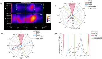
(a) Schematic of the experimental setup for the investigation of electron and proton acceleration by thin targets (gratings and planar surface). The IP stack is mounted on a motorized holder and can be vertically shifted. This allows access by a Thomson parabola spectrometer for proton acceleration measurements. (b) The top view of the IP stack shows the position relative to the target. (c) The IP stack sequence consists of IPs and aluminium filters of different thicknesses, which allows the detection of the electron spatial distribution for different energies. (d) A typical raw image of the IP signal. Here, θ and φ are the azimuthal and polar angles, respectively, used to describe the spatial distribution of the electrons.

The main diagnostic used in the study of electron acceleration was an image plate (IP) stack mounted in a cylinder holder of 6 cm radius. A schematic of the interaction geometry is shown in Figure 6(a), while the top view of the relative position of the target-stack is shown in Figure 6(b). The stack detector consists of four IPs (Fujifilm BAS-TR) separated by Al filters of different thicknesses (Figure 6(c)). The IPs with a size of 30 cm length and 9 cm height cover a large angular range around the interaction area within the limits defined by the azimuthal angle θ ∈ [18°, 342°] and the polar angle φ ∈ [–19°, 19°]. The first aluminium filter placed in front of the IP stack of 1.5 mm thickness ensures that the signal at the IPs is generated mostly by electrons, as 98% of the X-rays with photon energies up to 15 keV and electrons with energies E ≤ 800 keV are suppressed by the filter. The stack of IPs and Al filters allows the simultaneous recording of the spatial profile of the electron beam for several energies (E > 0.8, 1.2, 1.4 MeV and E > 1.4 MeV, respectively), a typical recorded signal being shown in Figure 6(d).
Examples of raw data using thin Au gratings are shown in Figure 7, where the spatial distribution of the high-energy electrons was recorded over a large angular range around the interaction point. The physical properties of the electron beams, such as the acceleration direction, collimation, energy and/or spatial distribution offer important information about the fundamental processes that accompany the laser–grating interaction. Hence, electrons accelerated along the target surface could reveal the fundamentals of plasmon excitation in the relativistic regime, while the physical parameters of the electron beams accelerated at the rear side of the target can disclose either the processes of energy laser coupling or the conversion efficiency of the laser energy to high-energy particle beams.
(a) Spatial distribution of the high-energy electrons accelerated by a thin planar Au FT foil (top) and a thin Au GT (bottom) irradiated by the laser pulse at 20° incidence angle. Here, the data correspond to IP2 (E > 1.2 MeV). (b), (c) The reconstructed angular distribution of the electrons for the planar foil (black) and grating (red) recorded by IP1 (E > 0.8 MeV) in similar interaction conditions as in (a) and for two laser incidence angles, 20° and 45°, respectively. (d) The distribution of the electrons as a function of emission angle for the planar foil (black) and grating (red) recorded by IP1 (E > 0.8 MeV) for the case of a 20° incidence angle.

For comparison, the spatial distribution of the electron beams recorded by IP2 (E > 1.2 MeV) for a GT and a flat thin (FT) foil of the same dimensions is shown in Figure 7(a). Both targets were irradiated under similar conditions by a laser pulse of 2 × 10²⁰ W/cm2 intensity and at 20° incidence angle. The initial signal intensity, called photostimulable luminescence (PSL), recorded by IPs was retrieved via a CR35BIO scanner with a 50 μm pixel size. The number of electrons was determined from the recorded PSL signal, following the calibration method described in Refs. [Reference Pham, Thuillier and Manach51,Reference Koval and Vac52], which gives the deposited energy per electron at normal incidence on the sensitive layers of various IPs. In case of the BAS-TR IP, electrons with an energy of 1 MeV deposit approximately 18 keV and leave behind a PSL value of 0.003. Note that a correction factor of 16 (4×4) was applied to account for the different pixel size of our scanner (50 μm) compared with 200 μm in Ref. [Reference Hidding, Pretzler, Clever, Brandl, Zamponi, Lübcke, Kämpfer, Uschmann, Förster, Schramm, Sauerbrey, Kroupp, Veisz, Schmid, Benavides and Karsch31]. By integrating the electron number over the polar angle φ, one can infer the number of electrons per radian accelerated over the full range of the azimuthal angle.
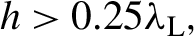
An example of the retrieved angular distribution is shown for both targets in Figures 7(b) and 7(c) corresponding to the signal recorded by IP1 (E > 0.8 MeV) for two laser incidence angles, 20° and 45°, respectively. Thus, the electron beams emitted by GT can have up to four times higher flux compared to the FT and better collimation for a specific emission direction (e.g., along the target surface). A similar result was observed for the 45° laser incidence angle, when the flux of the electrons accelerated along the target can be up to a factor of 2 larger in the case of GT compared with FT. For a better visualization of the electron flux emitted by the two targets, FT and GT, the electron angular distribution as a function of the emission angle θ is shown in Figure 7(d) in the case of a 20° incidence angle. The data have been obtained as well by the integration of the electron number over the polar angle φ from the raw signal recorded by IP1 (E > 0.8 MeV). Moreover, Figure 8 shows an overview of the total number of accelerated electrons (E > 0.8 MeV, emitted within the angle range θ ∈ [18°, 342°]), as well as the number of electrons contained within the bunches accelerated along the front (θ ∈ [250°, 260°]) and the rear surface of the target (θ ∈ [240°, 250°]). The thin gratings have an overall higher efficiency in accelerating electrons, by about a factor of 2, compared to the flat foils, and the charge of the accelerated electrons along the surface can reach 150 nC/rad.

Experimental results of laser energy absorbed fraction by micro-gratings (GT) and flat surface targets (FT) for various laser incidence angles.
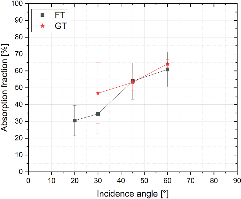
Accounting for the strong correlation of the electron acceleration and the efficiency of the laser energy coupling to the over dense targets, experimental investigations of the efficiency of the laser energy absorption by the micro-gratings in comparison with flat surface targets were carried out. The IP stack was replaced by an integrating Ulbricht sphere with a diameter of 20 cm coupled to a photodiode[ Reference Cerchez, Swantusch, Toncian, Zhu, Prasad, Toncian, Rödel, Jäckel, Paulus, Andreev and Willi 33 ]. In the linear regime of the sphere–photodiode system, the energy of the reflected laser beam was measured as a function of the laser incidence angle for both types of targets. The experimentally measured absorbed fractions for the investigated targets are presented in Figure 9. In the case of our micro-targets, for the investigated angles, the absorbed fraction shows a weaker dependence on the incidence angle compared with the flat target surface, while both targets reach at 60° laser incidence an absorption fraction larger than 60%. Note that in the current absorption measurements employing structured targets and using tight focused laser beams at small incidence angles (<30°), the absorption fraction can be overestimated. The focusing angle of the laser beam used in the experiment is approximately 28° and, due to the target surface modulation, part of the directly reflected beam can be scattered through the incoming laser port into the Ulbrich sphere.
In the coupling process of the laser energy to the targets of a periodically modulated surface, various physical effects can contribute and their interplay can be quite complex. The excitation of the SPWs and the geometrical surface effects can affect the global absorption fraction. For example, in the experimental study presented by Ceccotti et al.
[
Reference Ceccotti, Floquet, Sgattoni, Bigongiari, Klimo, Raynaud, Riconda, Heron, Baffigi, Labate, Gizzi, Vassura, Fuchs, Passoni, Květon, Novotny, Possolt, Prokůpek, Proška, Pšikal, Štolcová, Velyhan, Bougeard, D’Oliveira, Tcherbakoff, Réau, Martin and Macchi
5
], the laser energy absorbed fraction peaked around the resonant angle of the investigated grating and had a larger value compared with flat targets (no absolute values of the absorbed fraction were discussed). The results indicate that the resonant excitation of the SPWs leads to an enhanced laser energy absorption. In a numerical study, Cantono et al.
[
Reference Cantono, Sgattoni, Fedeli, Garzella, Réau, Riconda, Macchi and Ceccotti
17
] demonstrated that in the case of bulk GTs of depth $h>0.25{\lambda}_{\mathrm{L}},$
the number of energetic surface electrons decreases with the increase of h while the absorbed laser fraction increases for large values of grove depth. The study concludes that SPWs are less efficiently excited on gratings with deep grooves, despite increasing the target absorption, while the absorption is dominated by the geometrical effects above a certain depth value. As the vertical modulation of the gratings used in this study is
$h>0.25{\lambda}_{\mathrm{L}},$
the number of energetic surface electrons decreases with the increase of h while the absorbed laser fraction increases for large values of grove depth. The study concludes that SPWs are less efficiently excited on gratings with deep grooves, despite increasing the target absorption, while the absorption is dominated by the geometrical effects above a certain depth value. As the vertical modulation of the gratings used in this study is $h=400\;\mathrm{nm}$
, one might expect that the surface effects become more important for the laser energy absorption compared to the surface wave excitation. A GT irradiated at small incidence angles exposes a larger modulated surface to the laser interaction compared with a flat surface, and the surface topology leads to a higher value of the mean local incidence angle. Consequently, processes like vacuum heating can lead to an enhanced absorption compared with a planar target irradiated at the same nominal incidence angle. Moreover, additional surface effects such as, multiple reflections, can contribute to the increase of the absorption fraction[
Reference Tanaka, Yabuuchi, Sato, Kodama, Kitagawa, Takahashi, Ikeda, Honda and Okuda
57
] compared with a planar surface. At higher incidence angles, the contribution of effects previously mentioned is outweighed by shadowing effects due to the surface modulation, making both targets reach a quite similar global absorption level in grazing incidence geometries.
$h=400\;\mathrm{nm}$
, one might expect that the surface effects become more important for the laser energy absorption compared to the surface wave excitation. A GT irradiated at small incidence angles exposes a larger modulated surface to the laser interaction compared with a flat surface, and the surface topology leads to a higher value of the mean local incidence angle. Consequently, processes like vacuum heating can lead to an enhanced absorption compared with a planar target irradiated at the same nominal incidence angle. Moreover, additional surface effects such as, multiple reflections, can contribute to the increase of the absorption fraction[
Reference Tanaka, Yabuuchi, Sato, Kodama, Kitagawa, Takahashi, Ikeda, Honda and Okuda
57
] compared with a planar surface. At higher incidence angles, the contribution of effects previously mentioned is outweighed by shadowing effects due to the surface modulation, making both targets reach a quite similar global absorption level in grazing incidence geometries.
The number of electrons accelerated along the front surface (SFE) within the azimuthal angle $\theta \in \left[250{}^{\circ},260{}^{\circ}\right]$
as a function of laser angle of incidence (E > 0.8 MeV). The values are normalized to the number of SFE electrons recorded for a planar thin foil at 0° laser incidence angle.
$\theta \in \left[250{}^{\circ},260{}^{\circ}\right]$
as a function of laser angle of incidence (E > 0.8 MeV). The values are normalized to the number of SFE electrons recorded for a planar thin foil at 0° laser incidence angle.
Raw images of proton and ion traces detected by a Thomson parabola/MCP setup recorded for Cu targets: (a) micro-grating (GT) and (b) thin flat (FT). Comparison of the reconstructed energy spectra of (c) protons and (d) C+4 ions for the two types of targets.

The angular dependence of the electron acceleration efficiency along the target surface could offer an indication regarding the absorption mechanisms that could be sustained by self-induced surface fields and/or by SPWs. The number of accelerated electrons along the front grating surface as a function of the incidence angle is shown in Figure 10 for electron energies greater than 0.8 MeV. The data represent the number of accelerated electrons within an azimuthal angle of 10° above the target surface (N
SFE) and normalized to the electron number accelerated within the same azimuthal angle by a planar thin foil irradiated at normal incidence (N
SFE_FT0°). In the case of thin foils, the number of electrons accelerated along the front surface (SFE) has a very weak dependence on the laser incidence angle, in contrast to the angular dependence of the absorption fraction for this type of target. With regard to the micro-gratings, the flux of the accelerated SFEs shows higher values at intermediate angles up to a factor of 2 larger compared with the same conditions of interaction for planar foils. Due to the poor laser condition for the shots onto the GTs at 30° laser incidence, the data for this angle are not shown here. Note that for the results presented in Figure 10, no direct correlation between the angular dependence of the global absorption fraction (Figure 9) and of the electron acceleration efficiency along the target surface can be established. As observed in other studies, a possible explanation is related with the distribution of the laser energy along different electron acceleration channels via processes such as electron recirculation or surface fields developed with deep surface modulations. They are associated with the target thickness and they could not be deconvoluted from the present data. Further investigations addressing the energy spectral distribution of the accelerated electrons and the surface field structure could bring more understanding to the laser–micro-gratings interaction and will be presented in detail elsewhere. Moreover, the grating’s surface effects on the absorption and acceleration of the energetic electrons will require parametric studies of the role played by the grating topology, employing gratings with different groove depths h, surface periodicities ${\lambda}_{\mathrm{g}}$
and different aspect ratios
${\lambda}_{\mathrm{g}}$
and different aspect ratios $h/{\lambda}_{\mathrm{g}}$
.
$h/{\lambda}_{\mathrm{g}}$
.
Furthermore, we investigated the acceleration of proton beams via the target normal sheath acceleration (TNSA) mechanism on the rear side of a thin grating irradiated at normal incidence.
For these measurements we used cooper micro-gratings (Figure 4(a)) of 10 μm thickness, 2 μm grating periodicity and 400 nm vertical modulation. A Thomson parabola (TP) spectrometer coupled to a micro-channel-plate (MCP) detector was employed as a diagnostic tool and placed along the target normal and laser forward direction. The positioning of the TP is shown schematically in Figure 6(a). Thin flat Cu foils of the same thickness were irradiated in similar conditions, as a reference interaction. Images of protons and carbon ions (C+1, C+2, C+3, C+4) traces recorded by the MCP accelerated by micro-gratings and thin foils are presented in Figures 11(a) and 11(b). The energy spectra of the protons and C+4 ions presented in Figures 11(c) and 11(d) reveal the influence of the target topology on the physical parameters of the accelerated ion beam, such as the cut-off energy and the flux. In case of GT, the cut-off energy of the protons is about 8.3 MeV compared with 7.2 MeV in case of FT, while for the carbon ions, the cut-off energy is about 0.8 MeV/nucleon, almost a factor of 2 larger compared to FT. The enhanced ion beam properties can be attributed to the increased laser energy absorption at normal incidence as a modulated surface exposes a larger effective area to the laser irradiation. While this investigation has been limited by the chamber configuration to the normal incidence angle, further planned studies aim to investigate simultaneously the electron and ion energy spectra in various interaction conditions, at higher incidence angles. These studies of ion acceleration by the micro-targets are particularly relevant, as it was observed in previous works that ions’ cut-off energy and number are in a more complex way influenced by laser energy transfer to the hot electron population (see, e.g., Ref. [Reference Lübcke, Andreev, Höhm, Grunwald, Ehrentraut and Schnürer58], and the references herein).
The employment of the micro-structured thin foils in the high-power laser experiments operating at a high repetition rate raises questions related to the stability of target and holder positioning. In the experiments presented in this work, the micro-GTs have been placed in the interaction area in a free-standing mount or supported by a holder. In both configurations, the thin foils demonstrated robust handling in all preparation phases (cutting, transportation, pumping down, etc.) prior to interaction. The holder used in this experiment allows the mounting of nine micro-gratings, but there are no indications that holders with a larger number of targets would pose problems regarding the target’s survival or stability. In the case of a large size holder, the accuracy of target positioning in the laser focus can be ensured by the motorized target drivers. In a recent review[ Reference Prencipe, Fuchs, Pascarelli, Schumacher, Stephens, Alexander, Briggs, Büscher, Cernaianu, Choukourov, De Marco, Erbe, Fassbender, Fiquet, Fitzsimmons, Gheorghiu, Hund, Huang, Harmand, Hartley, Irman, Kluge, Konopkova, Kraft, Kraus, Leca, Margarone, Metzkes, Nagai, Nazarov, Lutoslawski, Papp, Passoni, Pelka, Perin, Schulz, Smid, Spindloe, Steinke, Torchio, Vass, Wiste, Zaffino, Zeil, Tschentscher, Schramm and Cowan 1 ], a number of valid solutions for this problem have been already implemented with a resolution of a few μm on target positioning in the laser focus.
4 Conclusions
In this study, a novel approach was addressed to successfully obtain micro-gratings patterned directly on thin free-standing Au and Cu foils, by means of EBL and Ar-ion milling techniques. The results from microscopic surface analysis techniques indicated the need of pre-processing of the as-received foils, specifically by cold rolling and surface plasma cleaning, before the grating fabrication. The major improvement of the surface roughness and flatness after cold rolling allowed a controlled and ordered structured surface to be obtained. Optimization of each step of the lithographic and dry etching processes allowed the achievement of 2 μm periodicity metallic gratings, of two different shapes: either rectangular or sinusoidal profiles. The processing method described in this paper can be used for yielding micro- or nano-sized gratings with dimensions limited only by the employed lithographic method. Preliminary experimental tests have shown the robust and easy integration of the micro-gratings as targets in high-intensity laser experiments. Moreover, the targets demonstrate their capability in providing experimental information relevant for the investigation of the laser–grating fundamentals as high-energy electron acceleration and laser energy coupling onto the periodically structured targets. Novel physical effects may be revealed when gratings are irradiated with ultra-relativistic laser pulses produced by the new laser facilities (Extreme Light Infrastructures[ Reference Tanaka, Spohr, Balabanski, Balascuta, Capponi, Cernaianu, Cuciuc, Cucoanes, Dancus, Dhal, Diaconescu, Doria, Ghenuche, Ghita, Kisyov, Nastasa, Ong, Rotaru, Sangwan, Söderström, Stutman, Suliman, Tesileanu, Tudor, Tsoneva, Ur, Ursescu and Zamfir 59 – Reference Margarone, Cirrone, Cuttone, Amico, Andò, Borghesi, Bulanov, Bulanov, Chatain, Fajstavr, Giuffrida, Grepl, Kar, Krasa, Kramer, Larosa, Leanza, Levato, Maggiore, Manti, Milluzzo, Odlozilik, Olsovcova, Perin, Pipek, Psikal, Petringa, Ridky, Romano, Rus, Russo, Schillaci, Scuderi, Velyhan, Versaci, Wiste, Zakova and Korn 63 ], APOLLON[ Reference Papadopoulos, Zou, Le Blanc, Chériaux, Georges, Druon, Mennerat, Ramirez, Martin, Fréneaux, Beluze, Lebas, Monot, Mathieu and Audebert 64 ], SULF[ Reference Mondal, Wei, Fareed, Hafez, Ropagnol, Sun, Kahaly and Ozaki 23 ], etc.).
Acknowledgements
This work was supported by the ELI-NP Phase II project, co-financed by the Romanian Government and the European Union through the European Regional Development Fund – the Competitiveness Operational Programme (contract No. 1/07.07.2016, COP, ID 1334). Funding from the National Program ‘Installations and Strategic Objectives of National Interest’ and ‘Nucleu’ project PN19060105 of the Romanian Government, as well as funding from the European Union Framework Programme for Research and Innovation Horizon 2020 under grant agreement No. 871161, are also gratefully acknowledged.
Supplementary Materials
To view supplementary material for this article, please visit http://doi.org/10.1017/hpl.2021.57.


 Open access