


Introduction
In the ever-evolving domains of space systems, mobile communications, and advanced radar technologies, there is a growing need for high-performance RF and microwave transmit/receive (T/R) front-end modules (FEMs). These modules must seamlessly combine wideband capabilities, low noise, and high power efficiency to address the demands of next-generation systems such as 5G networks. GaN-based MMICs have emerged as the preferred solution for developing compact, efficient single-chip FEMs, owing to their exceptional material properties, including a high breakdown electric field, superior power density, and low conduction resistance [Reference Lin, Wu, Chen, Hu, Chen and Zhang1].
Traditional GaN MMIC FEMs, which integrate PAs, LNAs, and RF switch components, have been developed across a range of frequency bands. Notable works in C-band monolithic integration have been highlighted in [Reference Lin, Wu, Chen, Hu, Chen and Zhang1–Reference Giofrè, Ciccognani, Colangeli, Feudale, Lanzieri, Polli, Salvucci, Suriani, Vittori and Limiti5]. However, many of these designs face challenges, including significant chip area consumption, insertion losses from external switches, or limited bandwidth, resulting in higher costs and reduced performance efficiency.
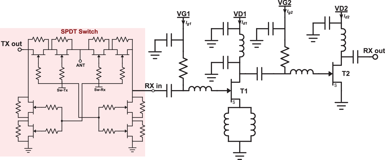
This paper presents a comparative study of two distinct GaN-HEMT process technologies, each featuring a unique digital transceiver (TRx) architecture. The first design, referred to as the LNAiS-based architecture, is fabricated using a 250 nm GaN-HEMT process and integrates a low-noise amplifier with switching capability (LNAiS) and a digital class-E power amplifier (PA) on a single compact chip (see Fig. 1 (right)). This integration eliminates the need for an external RF switch, significantly reducing frontend complexity and simplifies the design, achieving robust performance with minimal chip space. By combining low-noise amplification and high isolation within the LNAiS, this design achieves competitive performance, offering gain and noise figure comparable to or better than standard designs. Furthermore, the digital PA demonstrates exceptional flexibility and efficiency, capable of wideband operation up to 6 GHz with minimal modifications to the broadband output network [Reference Krishnaji Rao, Wentzel, Hoffmann, Schellhase, Chevtchenko and Rudolph6].
The second design, referred to as the switch-based architecture, adopts a more conventional approach and is implemented using a 150 nm GaN-HEMT process. It integrates the same concept of digital PA with a standard SPDT switch and LNA (see Fig. 1 (left)). The RF switch decouples the Tx and Rx paths, ensuring stable operating environments for both the PA and LNA. This traditional approach relies on added circuitry to achieve isolation, thus introducing additional integration losses and increased design complexity.
This paper builds upon prior work [Reference Krishnaji Rao, Wentzel, Hoffmann, Schellhase, Chevtchenko and Rudolph6] by introducing a comparison between two architectures implemented on distinct GaN-HEMT technologies. The LNAiS approach, by incorporating switching functionality directly into the LNA, eliminates the external RF switch and its associated losses. This integration not only reduces complexity but also minimizes parasitics, improves efficiency, and enhances scalability for future transceiver designs. Despite the traditional method’s robustness, the LNAiS architecture achieves comparable stability while offering significant advantages in flexibility, compactness, and simplicity. This work highlights the trade-offs between traditional and innovative approaches, showcasing the LNAiS architecture as a promising candidate for energy-efficient, scalable, and cost-effective RF front-end solutions for next-generation 5G networks.
Block diagram of conventional digital TRx (left) and proposed novel digital TRx including an LNAiS and digital class-E PA (right).

Gan HEMT technologies
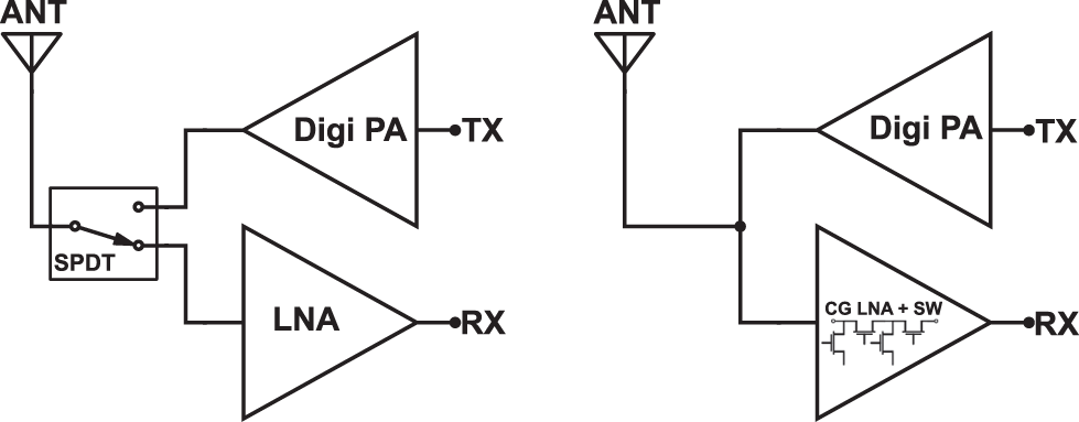
The digital transceiver MMICs were fabricated using two distinct GaN technologies of the Ferdinand-Braun-Institut (FBH), Berlin. The first technology features 250 nm gate-length devices and utilizes Al0.22GaN (22 nm)/GaN HEMTs epitaxial layers on 4-inch semi-insulating SiC substrates. In contrast, the second technology utilizes 150 nm gate-length devices with an Al0.28GaN (10 nm) barrier [Reference Osipov, Chevtchenko, Lossy, Bengtsson, Kurpas, Kemf, Würfl and Tränkle7].
The fabrication process involved FBH’s standard GaN HEMT technology steps, including the formation of source/drain ohmic contacts, deposition of a PECVD SiNx layer, device isolation via nitrogen ion implantation, and gate formation using a sputtered gate module with gate lengths of 250 nm or 150 nm. A 200 nm thick SiNx gate encapsulation layer was deposited, followed by the formation of interconnections. All transistors feature a 0.5 µm source-gate distance and a 2.0 µm drain-gate distance, consistent across the types. The 250 nm technology utilizes the FBH baseline process, whereas the 150 nm technology incorporated an optimized PECVD SiNx passivation layer, detailed in [Reference Yazdani, Beleniotis, Brunner, Ostermay, Würfl, Rudolph, Heinrich and Hilt8]. Figure 2 illustrates the key differences between the two GaN technologies.
Simplified cross-sections of the fabricated devices: 250 and 150 nm gate process technologies.

Digital TRx module architecture
The digital transceiver MMIC, combined with a frequency limiting output network, was designed for 5G operation from 3.7 to 6 GHz. It integrates the LNAiS for receiver mode and the digital PA for transmitter mode and was fabricated using 250 nm technology. For comparison, a standard transceiver MMIC, featuring a conventional SPDT switch and a two-staged standard LNA paired with the same digital PA concept, was fabricated using 150 nm technology. Importantly, the choice of different gate lengths was not intended to optimize TRx performance, but rather to facilitate comparison between a fully integrated transceiver without an external switch and a conventional architecture with a separate RF switch.
This section outlines the key building blocks of the transceivers, including the LNAiS, the standard LNA with separate SPDT switch, the digital PA, and the compact single-chip integration of both chip combinations.
Low-noise amplifier with integrated switch (LNAiS)
Figure 3 illustrates the schematic of the two-staged LNA with integrated switching functionality, designed and fabricated using the 250 nm process. Both stages of the LNA utilize 1 ×50 µm common-gate transistors. As part of the DC-supply network, a pair of 12 ×50 µm common-source bias-switching transistors (highlighted in Fig. 3) are employed to connect the sources of the RF stages to ground, enabling low-noise amplification during receiver (Rx) mode. In transmitter (Tx) mode, when the antenna needs to be isolated from the Rx path, the sources of the RF stages are disconnected from the ground dc-wise, forcing 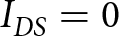 $I_{DS}=0\,$mA, which turns off the HEMTs in both stages. The operating mode of the LNAiS is controlled by the voltage $V_\textrm{Switch}$, which is set to 0 V for Rx mode or −5 V for Tx mode. To enhance ruggedness, the gates are fed through high-resistance elements (2 kΩ). This design forces the input stage of the LNA into a deep class-C mode at high input powers, protecting the circuit during RF overload situations when the gate diode becomes conductive and positive gate current flows, as described in [Reference Rudolph, Behtash, Doerner, Hirche, Wurfl, Heinrich and Trankle9].
Schematic of the LNA with integrated switching capability (LNAiS).

When the LNAiS is integrated with the PA to form the TRx frontend module, the LNA in its OFF state may load the output of the PA connected to the common antenna port. Unlike traditional architectures with an external RF switch, the absence of a dedicated decoupling mechanism between the Tx and Rx paths can lead to mutual interaction, potentially causing signal degradation or detuning of the PA and LNA. To mitigate this effect, the input matching of the LNAiS is optimized to minimize capacitive loading, providing a near open-circuit condition. This ensures minimal impact on the PA’s performance, consistent with the approach outlined in our prior work [Reference Krishnaji Rao, Doerner, Yazdani and Rudolph10, Reference Krishnaji Rao, Doerner, Chevtchenko, Haque and Rudolph11].
Standard LNA with separate SPDT switch (LNAsS)
In comparison to the LNAiS, the integration of standard SPDT switch and LNA MMIC is designed for evaluation using the 150 nm process. The schematic of the standard SPDT switch and LNA is shown in Fig. 4.
The standard SPDT switch MMIC (highlighted in Fig. 4) facilitates the transceiver’s ability to alternate between the receive and transmit paths by turning the respective path ON or OFF. By reversing the biasing conditions, the SPDT switch can control two distinct circuits and dynamically change the signal path. The implemented topology adopts a reflective series-shunt configuration, optimized for wideband operation. Control voltages of 0 V and −20 V are employed to activate and deactivate the selected path. To achieve low insertion loss and high isolation, the switch is designed using transistors of 8 × 1000, 6 × 750, and 4 × 500 µm. The classical SPDT switch design achieves an insertion loss of less than 1 dB within the band of interest while providing effective isolation between the antenna and receive path, along with robust power-handling capabilities.
Schematic of the standard LNA with separate SPDT switch (LNAsS).

The combined LNA is a two-staged amplifier developed using 12 × 50 µm common-source transistors. This configuration is optimized to minimize the noise figure while delivering maximum gain. The first stage employs source degeneration inductors to maintain circuit stability and optimize noise matching, while the second stage enhances the amplifier’s overall gain performance. This design ensures flat gain and low noise across the 5G frequency range. Additionally, the biasing network is carefully optimized for stability, with gate biasing applied through a high-resistance element of 2 kΩ to improve the ruggedness of the LNA. A similar approach using separate chips was presented in our previous work [Reference Krishnaji Rao, Wentzel, Andrei and Rudolph12].
Digital class-E power amplifier
Following the previously described LNA configurations, the digital PA is designed and integrated into the transmit path of the transceiver MMIC, working alongside either LNA setup to efficiently amplify signals. This PA concept is implemented in both 250 and 150 nm technologies. Although the underlying transistor parameters differ due to the respective technologies, the overall PA design remains consistent.
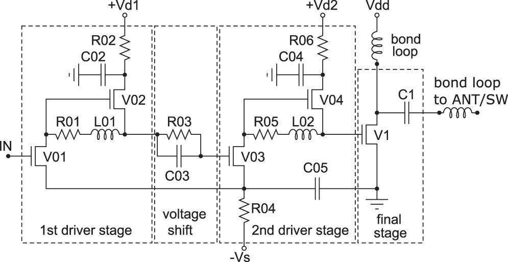
The digital class-E PA, shown in Fig. 5, utilizes a two-staged driver circuit with identical structures to effectively drive the 16 × 125 µm common-source GaN final-stage transistor (V1). This approach is comparable to the design presented in our previous publication [Reference Hoffmann, Schellhase, Heinrich and Wentzel13].
Schematic of the GaN digital class-E PA including 2-staged drivers and common-source final-stage.

The first driver stage employs an input GaN-HEMT transistor (V01) in a source configuration. An active pull-up circuit, consisting of V02, R01, and L01, complements this stage. The values of R01 and L01 are carefully selected to ensure short switching times. The resistor R02 damps ringing caused by the resonance circuit formed by bond wires and on-chip RF blocking capacitors (C02 and C04). A parallel circuit with R03 and C03 functions as a voltage shifter, eliminating the need for an additional power supply and thereby reducing the form factor of the DC circuitry.
For the second driver stage, the components R05 and L02 are designed with lower impedances to ensure rapid switching of the gate of the final-stage transistor (V1). A capacitor (C04) connected to ground and a resistor (R06) at the drain provide RF blocking for the DC path and dampen any ringing.
Finally, the typical class-E-like output network is formed using bond wires and the output capacitor (C1), which subsequently connects to either the LNAiS or the standard SPDT switch. It is important to note that in this work, emphasis was on proper switching of the final-stage transistor and not on minimizing DC power consumption of the drivers.
Compact single-chip integration
Two transceiver MMICs were fabricated to enable comparison between different circuit combinations. In the first configuration (see Fig. 6), the LNAiS and digital PA are integrated in a single chip using 250 nm technology. The two circuits, the LNA and PA, are connected to the common antenna port via the final-stage output inductance of the PA, which serves as part of the matching network. This inductance is located between C1 (see Fig. 5) and the on-chip output pad. This inductance, along with the final-stage drain bias feed, is realized using bond-wire loops. Additionally, the design includes a footprint for a 008004 $^\prime$$^\prime$ SMD capacitor on the output pad, allowing a filter capacitor to be directly soldered onto the chip, thereby preventing impedance mismatches caused by extended connections.
The second configuration integrates the digital PA with a standard SPDT switch and LNA combination (LNAsS) on a separate transceiver MMIC using 150 nm technology, as illustrated in Fig. 7. In this design, the PA’s output is connected to the transmit path of the standard SPDT switch via bond-wire loops. The SPDT switch alternates between the Tx and Rx paths based on the appropriate biasing conditions.
Both designs were fabricated for a comprehensive comparison of their performance and functionality, showcasing the impact of switch integration techniques on the overall transceiver module efficiency and effectiveness.
Hybrid transceiver module
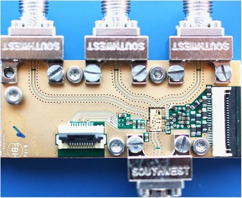
The digital TRx chip, whether configured as shown in Fig. 6: LNAiS connected to digital PA or Fig. 7: LNAsS to digital PA, was mounted on a copper heat sink and connected via bond-wires to a 0.25 mm Rogers 4003C PCB laminate containing hybrid input, output, and biasing networks. All off-chip passive elements were soldered on the PCB. Furthermore, the input of the digital class-E PA is fed with two parallel 50 Ω lines, which leads to an effective 25 Ω source impedance driving of the input GaN-HEMT V01 (see Fig. 5). Figure 8 shows the assembled module. Observing Fig. 8, we have to state that the compact module size of 20×50 mm2 would be even more reduced if smaller SMA connectors were used. However, this proves the great potential of the proposed digital TRx circuit in terms of reducing form factor and thus CO2 footprint.
Photograph of the compact digital TRx GaN MMIC integrating the LNAiS and digital PA fabricated using 250 nm technology; size: 4.5 × 2.34 mm2.

Photograph of the compact digital TRx GaN MMIC including LNAsS and digital PA fabricated using 150 nm technology; size: 4.5 × 2.4 mm2.

Photograph of realized transceiver module (size: 20 × 50 mm2).

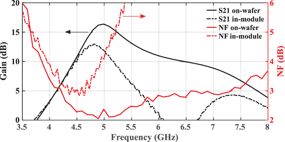
Gain and noise figure of the LNAiS measured: on-wafer (solid) and coaxially in-module (dotted).

Measurement results
Receiver mode: LNAiS
Before integration of the TRx MMIC into the hybrid module, the LNAiS was characterized on-wafer in both its receiver and isolation operational modes, utilizing dedicated RF pads specifically designed for wafer-level measurements.
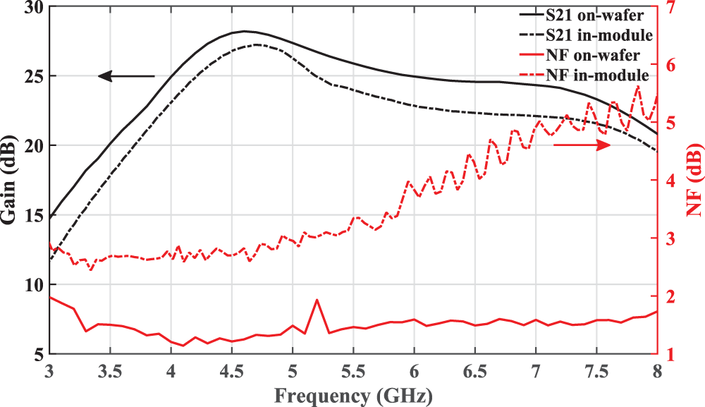
For low-noise amplification operation in Rx mode, drain bias voltage and current in both stages are set to 20 V and 60 mA, respectively with  $V_\textrm{Switch}=0\,$V. These quiescent points were achieved at $V_\textrm{G1,2}=-2.69\,$V (see Fig. 3). Figure 9 presents the on-wafer and module measurements of gain and noise figure. Measured on-wafer, the LNAiS shows gain of 14 dB at 4.7 GHz and 16.3 dB at 5 GHz. And, noise figure of 2.17 dB at 4.7 GHz and 2.35 dB at 5 GHz. Whereas, measured coaxially in-module, 12.7 dB gain and noise figure of 3 dB at 4.7 GHz are obtained. The input matching ( $S_\mathrm{11}$) and output matching ( $S_\mathrm{22}$) values are below −10 dB from 4.5 to 5 GHz for both on-wafer and coaxially in-module measurements. The observed frequency shift, gain reduction, and increase in noise figure in coaxially in-module measurements can be attributed to a certain detuning due to the parallel connection of the PA output, namely its aforementioned bond-wire inductor.
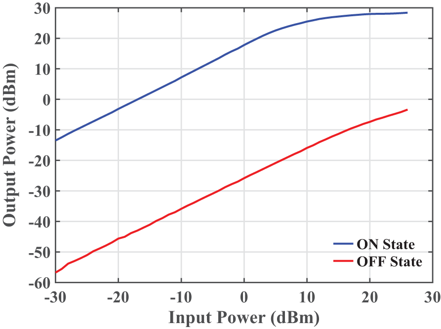
To evaluate the robustness and isolation for high power operation, on-wafer power measurements were performed, as shown in Fig. 10. It is seen that the LNA in amplification mode saturates for  $P_\mathrm{in} \gt $ 10 dBm and limits the output power to approximately 28 dBm (blue curve), thus protecting itself and subsequent stages from high input powers, even if it is not switched off. In the OFF state, isolation better than 20 dB is achieved for the frequency range of 4.7 GHz up to 7.4 GHz for small-signal conditions. Additionally in high power, it effectively reduces $P_\mathrm{in}$ below 0 dBm up to $P_\mathrm{in}=$ 27 dBm (red curve).
On-wafer power measurements of the LNAiS at 5 GHz: LNA operation (“ON state,” blue line) and isolation operation (“OFF state,” red line)

Gain and noise figure of the standard LNA measured: on-wafer (solid) and coaxially in-module (dotted).

Receiver mode: standard LNA with SPDT switch
The RF measurements for the standalone LNA MMIC were carried out directly on the wafer, with the device operating under a drain voltage of 15 V and a drain current of 80 mA for each stage. The highest gain was observed at 4.6 GHz, where the LNA achieved 28.2 dB with a noise figure of 1.25 dB. At 4.2 GHz, the gain was 26.6 dB and a noise figure of 1.28 dB. Across the broader frequency range of 4–6 GHz, the amplifier demonstrated consistent performance, delivering a gain exceeding 25 dB and an average noise figure of 1.5 dB. Additionally, return losses  $S_\mathrm{11}$ and $S_\mathrm{22}$ were both greater than 10 dB from 4.6 to 6.4 GHz.
Subsequent measurements were carried out for the fully integrated transceiver chip using coaxial in-module testing. The testing conditions were consistent with those used for the standalone LNA measurements. In this setup, the SPDT switch was connected in Rx mode, with a biasing voltage of 0 V to activate the Rx path and −20 V to deactivate the Tx path. For the integrated module, a gain of 28.2 and 2.7 dB were seen at 4.7 GHz, while at 4.2 GHz, the gain was 24.8 dB and the noise figure was 2.65 dB. The curves comparing the performance of the standalone LNA and the integrated transceiver chip are shown in Fig. 11. The observed drop in gain and increase in noise figure by more than 1 dB can be attributed to the inclusion of the integrated switch and the associated integration losses.
Additionally, it is important to note that the differences in GaN-HEMT process technologies used for the standard LNA (150 nm) and the LNAiS (250 nm) inherently influence their performance. The 250 nm process, with its higher breakdown voltage, enhances the LNAiS’s power-handling capability, but results in slightly lower gain and a higher noise figure due to increased parasitics. Conversely, the 150 nm process, with its shorter gate length, enables the standard LNA to achieve higher gain and lower noise, benefiting from improved electron confinement. However, the standard LNA requires an external RF switch for Tx/Rx isolation, introducing additional complexity and insertion losses.
Transmitter mode: digital class-E PA in 250 nm technology
All measurements of the integrated digital class-E PA from 250 nm GaN technology have been conducted coaxially in-module while applying  $V_\textrm{Switch}=-5\,$V in order to switch the LNAiS into attenuation mode. At the optimum operation frequency of 4.7 GHz, the amplifier has been characterized with single-tone as well as modulated signals. All input signals were generated with a digital modulator concept comparable to [Reference Hühn, Wentzel and Heinrich14]. It includes an inline linearization technique which does not consume any additional energy (unlike usual DPD) significantly reducing Tx, and thus TRx power consumption. The Matlab-implemented code feeds the AWG in the measurement setup which drives the PA input with binary bit streams.
Summary of modulated measurements of digital class-E PA with LNAiS in OFF stage (VSwitch = −5 V); VDD = 10 V.

Measured AM-AM and AM-PM distortion characteristics of digital TRx output signal from Fig. 12; EVM (rms): 9.7%; EVM (max): 36%.

Measured AM-AM and AM-PM distortion characteristics of digital TRx output signal @ 4.2 GHz carrier for a 20 MHz OFDM signal (9 dB PAPR);  $V_{DD} = 10\,V$; EVM (rms): 10.7%; EVM (max): 36.9%.

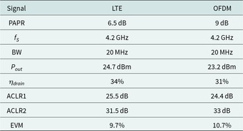
Maximum output power (Pout) of PA is 1.6 W (32 dBm) at a final-stage drain supply voltage (VDD) of 12 V. The final-stage drain efficiency (η drain) reaches 57% at this Pout. The low VDD value operates the PA in a safe region when taking maximum  $3.6\cdot V_{DD}$ voltage swing across the final-stage according to class-E theory into account. For operation in real mobile communication scenarios, it is essential to check the PA with modulated measurements. We tested LTE and OFDM input signals, all at VDD of 10 V, with bandwidths from 20 MHz up to 240 MHz. For reference, the maximum Pout at 1-tone input signal is 30.3 dBm at 10 VDD with an efficiency of 57%. Table 1 summarizes the results for a signal bandwidths (BW) with regard to Pout, ηdrain, adjacent channel leakage ratio (ACLR) in first two sidebands and error vector magnitude (EVM), all for a certain encoded peak-to-average power-ratio (PAPR).
The digital PA efficiency peaks at 46% for a 20 MHz LTE signal at 23.8 dBm of output power. Using a more 5G-like signal like 20 MHz OFDM with a higher PAPR of 9 dB the efficiency decreases to 25% at a respective lower Pout of 20.6 dBm. For a very wideband 240 MHz OFDM signal an ηdrain of 22% has been achieved. In order to prove the flexibility of the PA, we also conducted LTE measurements (6.5 dB PAPR) at a lower frequency of 3.7 GHz. Here the PA reaches 37% efficiency. Considering the innovative concept of the digital PA with LNAiS, the results achieved in this study further validate its potential and reinforce its promising performance, as previously demonstrated in [Reference Krishnaji Rao, Wentzel, Hoffmann, Schellhase, Chevtchenko and Rudolph6].
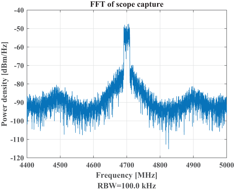
Furthermore, Table 1 shows that the linearity (ACLR, EVM) does not yet meet 3gpp requirements. Fig. 12 presents the output spectrum for the 20 MHz OFDM input signal (9 dB PAPR) at 4.7 GHz. It clearly shows low ACLR values (23 and 28 dB) of the output signal in the form of pronounced shoulders in the first two sidebands. EVM values of 9.7% (rms) and 36% (max.) have been reached, respectively. One reason for these linearity values is that due to couplings between bond-wire loops of PA output and LNA as well as not yet optimized filtering of the wanted signal at amplifier output, the input for the linearization algorithm itself gets distorted. This limits the reachable ACLR in the actual implementation. Further work will improve the linearity with refined parameters and adjusted linearization algorithm, always along with a feasible hardware implementation and realistic parameters, e.g., in oversampling rates. Again, for the experimental test of such a digital GaN-based transceiver module, the performance achieved is promising and proves its potential for future green 5G networks.
Measured output spectrum of digital Tx @ 4.7 GHz carrier for a 20 MHz OFDM signal (9 dB PAPR);  $V_{DD} = 10\,V$; Pout = 20.6 dBm.

Transmitter mode: digital class-E PA in 150 nm technology
The measurements of the integrated digital class-E PA along with LNAsS, implemented with 150 nm GaN technology, were conducted coaxially in-module in the Tx mode of the SPDT switch. The switching path in Tx mode operates as the reverse of the Rx mode, with a bias voltage of 0 V used to activate the Tx path and −20 V to deactivate the Rx path. At the optimal operating frequency of 4.2 GHz, the amplifier was characterized using both single-tone and modulated signals, as described in detail in Section TXmode.
The maximum output power (Pout) of the PA is 1.63 W (32.14 dBm) at an operating frequency of 4.2 GHz with a final-stage VDD of 10 V. At this Pout, the final-stage drain efficiency (ηdrain) reaches 52%.
To evaluate the performance, we tested LTE and OFDM input signals at a consistent VDD of 10 V, with the bandwidth of 20 MHz. These tests were conducted using only one input bond loop connected to the PA, matched to a 50 Ω input. Based on the above reference of maximum Pout for a single-tone input signal, Table 2 summarizes the results.
Summary of modulated measurements with 20 MHz signals of digital class-E PA with LNAsS in Tx mode; VDD = 10 V.

The digital PA achieves a peak efficiency of 34% for a 20 MHz LTE signal, delivering an output power of 24.7 dBm. However, with a 20 MHz OFDM signal with a higher PAPR of 9 dB, the efficiency decreases to 31%, corresponding to a lower Pout of 23.2 dBm. Additionally, LTE measurements were performed at a lower frequency of 4 GHz, where the PA demonstrated an improved efficiency of 38%.
While the circuit design remains fundamentally unchanged, it is important to highlight that the fabrication technology and the specific configuration of the TRx MMIC significantly impact the behavior of the class-E PA. These factors introduce variations in key performance characteristics such as frequency, efficiency, output power, and linearity. Additionally, it is observed that 150 nm technology offers less flexibility in shifting the frequency using the flexible output network of this PA compared to 250 nm technology. Nonetheless, despite these modifications, the overall performance remains comparable to the 250 nm GaN technology implementation.
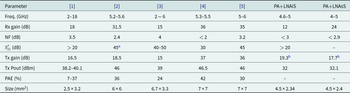
The performance of the proposed TRx MMIC, is compared to the conventional TRx MMIC presented in this paper and with existing transceivers, as shown in Table 3. The goal of this comparison is to assess the impact of integrating an LNA with switching capability (LNAiS) versus Switch-based MMIC. The results show that the LNAiS-based approach achieves comparable low-noise amplification and isolation while eliminating the need for a discrete RF switch, simplifying the transceiver architecture, and reducing insertion losses.
Comparison of the proposed MMICs with state-of-the-art.

a Simulation.
b Voltage gain.
To ensure robustness, large transistors were used in LNAiS, but future designs will implement smaller transistors while maintaining the same concept for improved compactness. Although both TRx chips have similar overall sizes, it is important to note that the LNAiS was implemented in 250 nm GaN technology, whereas the LNAsS used 150 nm technology, inherently making it smaller.
This study provides a design trade-off analysis, demonstrating that LNAiS-based transceivers offer a strong alternative for compact, switch-free designs. Future optimizations will focus on further miniaturization with improved performance.
Conclusion
Two GaN-based integrated digital transceiver concepts for 5G applications have been designed, fabricated, and measured. The two MMICs, fabricated using 250 and 150 nm gate length GaN-HEMT processes, were evaluated to compare their performance and efficiency.
The LNAiS-based architecture, integrates, an LNA with integrated switching capability (LNAiS) and a digital class-E PA circuit into a single compact chip using 250 nm technology. This novel design eliminates the need for an external antenna switch, thereby reducing frontend complexity and wafer space requirements. In Rx mode, the LNAiS achieves a low noise figure of 2.17 dB (on-wafer) and a gain of 14 dB at 4.7 GHz, while providing high isolation exceeding 20 dB in Tx mode. The integrated digital class-E PA demonstrates efficiencies of 46% and 25% for 20 MHz LTE (6.5 dB PAPR) and OFDM (9 dB PAPR) input signals, respectively, and delivers a maximum output power of 32 dBm at 12 V drain supply voltage for a 1-tone input signal. The flexibility of the digital PA is further demonstrated by achieving 37% drain efficiency at 3.7 GHz with a 20 MHz LTE signal, showcasing its adaptability across frequencies. While the linearity of the PA requires further optimization for practical applications, this TRx MMIC demonstrates promising performance with a compact and efficient architecture.
The switch-based MMIC combines the digital PA with a standard LNA and an SPDT switch (LNAsS), using 150 nm technology, forming a more conventional transceiver design for comparative evaluation. In Rx mode, this configuration achieves a gain of 24.8 dB and a noise figure of 2.65 dB at 4.2 GHz. In comparison, the standalone LNA at 4.2 GHz, achieves a gain of a 26.6 dB with noise figure of 1.28 dB. The additional circuitry in this design introduces more than 1 dB of integration losses, while the digital PA performance remains comparable to its implementation in the 250 nm GaN technology.
Overall, the proposed LNAiS-based digital TRx concept offers significant advantages, including reduced complexity, wafer space savings, high flexibility in the Tx chain, and a reduced bias supply requirement for switching. By eliminating the need for an antenna switch, this architecture represents a greener solution for future 5G networks, combining competitive performance with compact and efficient design. While the Switch-based configuration provides valuable insights into the trade-offs of conventional designs, the LNAiS-based chip demonstrates the potential of integrated digital transceivers to redefine the standards of next-generation communication systems.
Acknowledgements
The authors would like to thank their colleagues Steffen Schulz and Ralf Doerner for performing the measurements, and Bernd Janke for layout support at FBH. Financial support by Deutsche Forschungsgemeinschaft (DFG) under grant no. WE6288/3-1, RU1203/17-1 is gratefully acknowledged. Further, this work was partly funded by the German BMBF within the “Forschungsfabrik Mikroelektronik Deutschland (FMD)” framework under ref. 16FMD02 as well as within the project “GreenICT@FMD” under ref. 16ME0505.
Competing interests
The authors declare none.

Megha Krishnaji Rao received Bachelor’s degree in Telecommunications Engineering in 2016 from India and her Master’s degree in Electrical Engineering in 2020 from Hochschule Bremen, Germany. She is currently a final-year Ph.D. student at Brandenburgische Technische Universität (BTU), Cottbus, and a scientific researcher at Ferdinand-Braun-Institut gGmbH (FBH), Berlin. Her research focuses on designing, analyzing, and integrating a robust receiver with a digital PA in GaN technology into a single-chip transceiver for 5G. She has been a member of IEEE MTT-S since 2020 and, in 2024, joined the EuMA Innovation Team and also, serves as an associate software officer for EuMW 2025.

Andreas Wentzel (M’16) received the Diploma and the Doctoral degree in electrical engineering from the Technical University of Berlin, Germany, in 2006 and 2011, respectively. Since 2015 he has been the head of the Digital PA Lab in the III-V-Electronics department of the Ferdinand-Braun-Institut in Berlin, Germany. His research activities focus on the design, realization and measurements of flexible digital TX architectures, including advanced switch-mode power amplifier concepts realized on GaN and InP from GHz to sub-THz as well as on optimized modulation schemes suitable for these types of PAs. Moreover, his focus is on GaN- and AlN-based highly-efficient VHF power converters up to GHz-range. Dr. Wentzel is a member of IEEE and MTT society.

Thomas Hoffmann received the diploma from the Technical University of Dresden, Germany. Since 1983, he has worked as a design engineer in the research institute Zentrum für Wissenschaftlichen Gerätebau, in several companies, and as a freelancer. There, he developed electronic components and devices for industrial use, particularly switch-mode converters. Since 2008, he has been working for the Ferdinand-Braun-Institut (FBH) at Berlin, Germany as a research assistant, where he is developing drivers for pulse laser systems and, since 2015, digital power amplifiers.

Lars Schellhase received his diploma in 2006 from Siemens AG, Bereich Corporate Technology, Materials and Microsystems in Berlin. Since 2007, he has been working at FBH, specializing in DC characterization and packaging, contributing to advancements in semiconductor technology. In 2004, he gained valuable industry experience as a trainee at Samsung SDI Germany GmbH. With a strong background in materials and microsystems, he continues to play a key role in semiconductor research and development.

Serguei A. Chevtchenko received his diploma degree in solid state physics from Moscow Engineering Physics Institute, Moscow, Russia, in 1998, and the Ph.D. degree in engineering from Virginia Commonwealth University, Richmond, VA, USA, in 2007, where he conducted experimental studies of structural, optical, and electronic properties of wide bandgap semiconductors (GaN and ZnO). In 2008, he joined Ferdinand-Braun-Institute (FBH), Berlin, Germany. His responsibilities at FBH include the development and technical coordination of processes for the fabrication of GaN-based MMICs and high-power microwave transistors as well as the analysis of dc and microwave characterization results.

Hossein Yazdani received his B.Sc. degree in Electrical Engineering (Electronics) from Sheikh Bahaei University, Iran, in 2013 and his M.Sc. in Micro and Nano Systems from Chemnitz University of Technology, Germany, in 2018. He earned his Ph.D. degree from the Technical University of Berlin in 2024, by conducting research at the Ferdinand-Braun-institute (FBH) in Berlin, Germany. His current research focuses on the development of mm-wave devices, including the characterization, fabrication, and material technology of GaN-based devices.

Matthias Rudolph Matthias Rudolph received the Dipl.-Ing. degree in electrical engineering from the Berlin Institute of Technology, Berlin, Germany, in 1996, and the Dr.-Ing. degree from Darmstadt University of Technology, Darmstadt, Germany, in 2001. In 1996, he joined Ferdinand-Braun-Institut, Leibniz Insitut für Höchstfrequenztechnik (FBH), Berlin. In October 2009, he was appointed the Ulrich-L.-Rohde Professor for RF and Microwave Techniques at Brandenburg University of Technology, Cottbus, Germany. His research focuses on the modeling of FETs and HBTs and on the design of power, broadband, and low-noise amplifiers. He authored or coauthored over 100 publications in refereed journals and conferences and six textbooks. Dr. Rudolph was the Program Chair of the European Microwave Weeks 2007 and 2013, Chair of the German Microwave Conference 2010 and 2020, Electronic Submissions Chair of the European Microwave Week 2010-2011, of the IEEE COMCAS in 2013, 2017–2023, and of the Microwave and Radar Week in Krakow, 2016. 2012–18, he was the EuMA Conference Software Officer, and EuMA Deputy Conference Software Officer in 2018-2024. 2007–2024, he served at the IEEE MTT-S technical committees MTT-2 (CAD), MTT-11 (low-noise techniques, chair 2018-20) and was a member of the technical program review committe of the IEEE Intl. Microwave Symp. 2007–2020. 2020–2023, he was associate editor of the IEEE Trans. Microwave Theory Tech.


 Open access